 Embedded HandbookApps
15а. The new-style ADC on the G4: differential input, oversampling to 16 bits, two calibrations
Section 14 covered the ADC of the F1 and F4 and, separately, the simplified ADC of the F0 and G0 (14.10).
The G4, L4, H7 and U5 have an ADC of a different generation: the registers CR, ISR and CFGR instead of
CR1 and CR2, a regulator that has to be switched on, deep power-down after reset,
differential inputs, hardware oversampling to 16 bits, offset
and gain correction right in the block. Here — on the G474: what this gives, how to
switch it on at register level and where this ADC trips up someone porting code.
Prerequisites: reference manual RM0440 (G4, ADC chapter) and the STM32G474 datasheet (DS12288) from the Keil pack, the G4 LL header. The table of oversampling results from RM0440 was reproduced in full by calculation; the code was built with armclang for the G474. QEMU does not model this ADC.
Terms used in the documentation
Term Meaning single-ended, differential input input measured against ground, or as a difference of two pins oversampling ratio (OVSR), shift (OVSS) how many conversions to sum and by how many bits to shift the sum ADCALDIF calibration for differential inputs CALFACT_S, CALFACT_D calibration factors: single-ended and differential deep power-down (DEEPPWD) the ADC's deep sleep after reset voltage regulator (ADVREGEN) the ADC's internal regulator gain compensation (GCOMP) gain correction: the code is multiplied by a factor offset (OFRy) subtracting a constant offset from the result
15а.1 What is new compared with the F4
The G474 has five 12-bit ADCs; the datasheet promises a conversion in 0.25 µs and up to 16 bits with hardware oversampling. Differences from the F1 and F4:
- after reset the ADC is in deep power-down (
DEEPPWD= 1) with the regulator off: first clear DEEPPWD, switch onADVREGENand wait 20 µs (LL_ADC_DELAY_INTERNAL_REGUL_STAB_USin LL); - two calibrations: separately for single-ended and for differential inputs;
- a differential input on any channel that has a pair;
- oversampling — a sum of up to 256 conversions with a shift, up to 16 bits in the data register;
- offset (four
OFRyregisters) and gain correction (GCOMP) inside the block.
The registers are different: code from the F4 (CR2, SQR3) will not build — and that is good,
the error is visible at once.
15а.2 Clock and conversion time
The time of one conversion (RM0440, 21.4.12):
TCONV = sampling time + 12.5 ADC clock cycles.
The shortest sampling time is 2.5 cycles, the longest 640.5. The ADC clock per the datasheet is no higher than 60 MHz for a single ADC (52 MHz if all are running with VDDA of at least 2.7 V):
| ADC clock | Sampling | Conversion | Conversions per second |
|---|---|---|---|
| 60 MHz | 2.5 | 0.250 µs | 4.000 million |
| 52 MHz | 2.5 | 0.288 µs | 3.467 million |
| 42.5 MHz | 2.5 | 0.353 µs | 2.833 million |
| 60 MHz | 640.5 | 10.883 µs | 0.092 million |
The clock is selected by CKMODE in the common register ADC12_COMMON->CCR (RM0440, 21.4.3):
00 — a separate asynchronous clock from RCC (system or PLL "P"), 01, 10, 11 —
HCLK divided by 1, 2 or 4. On the G474 HCLK is up to 170 MHz, so HCLK / 1
and HCLK / 2 are too fast for the ADC; synchronously HCLK / 4 = 42.5 MHz remains.
For 60 MHz and 0.25 µs an asynchronous clock from the PLL is needed. The synchronous clock is good
for something else: the delay from a timer event to the start of conversion has no jitter.
15а.3 Enabling and two calibrations
Calibration on the G4 is mandatory and is done with the ADC disabled (ADEN = 0).
The factor for single-ended inputs and for differential ones is different
(RM0440, 21.4.8): the ADCALDIF bit selects which one to compute. If the ADC is going
to measure both kinds, calibrate twice — and from then on the ADC itself applies
the right factor when switching between channels:
void adc_power_and_calibrate(void)
{
    RCC->AHB2ENR |= RCC_AHB2ENR_ADC12EN;
    ADC12_COMMON->CCR = 3u << ADC_CCR_CKMODE_Pos;   /* HCLK / 4: 170 / 4 = 42,5 МГц, не больше 60 */
    ADC1->CR &= ~ADC_CR_DEEPPWD;                    /* после сброса АЦП в глубоком сне */
    ADC1->CR |= ADC_CR_ADVREGEN;
    wait_us(20);                                    /* LL_ADC_DELAY_INTERNAL_REGUL_STAB_US */

    ADC1->CR &= ~ADC_CR_ADCALDIF;                   /* 1: несимметричные входы → CALFACT_S */
    ADC1->CR |= ADC_CR_ADCAL;
    while (ADC1->CR & ADC_CR_ADCAL) {
    }
    ADC1->CR |= ADC_CR_ADCALDIF;                    /* 2: дифференциальные → CALFACT_D */
    ADC1->CR |= ADC_CR_ADCAL;
    while (ADC1->CR & ADC_CR_ADCAL) {
    }
    ADC1->CR &= ~ADC_CR_ADCALDIF;

    ADC1->ISR = ADC_ISR_ADRDY;
    ADC1->CR |= ADC_CR_ADEN;
    while (!(ADC1->ISR & ADC_ISR_ADRDY)) {
    }
}
The factors — 7 bits each — are kept in ADC_CALFACT. ADC power
is lost in Standby and VBAT, and the calibration with it; to avoid calibrating
again, they can be saved and written back (RM0440, 21.4.8).
15а.4 Differential input
A channel's bit in DIFSEL switches it to differential mode; DIFSEL
may only be written with the ADC disabled. The code according to RM0440:
a difference of −VREF+ gives 0x000, zero gives 0x800, +VREF+ gives 0xFFF. That is
code = 2048 + 2048 × (VINP − VINN) / VREF+.
| VINP − VINN at VREF+ = 3.3 V | Code |
|---|---|
| −3.3 V | 0x000 |
| −1.0 V | 0x593 |
| 0 | 0x800 |
| +1.0 V | 0xA6D |
| +3.3 V | 0xFFF |
One code is 1.611 mV against 0.806 mV for a single-ended input: the RM states plainly that the sensitivity is half as high. On the other hand common-mode interference is subtracted, and the sign of the difference is visible at once. Both inputs must be kept around VREF+/2 — the common-mode voltage must not wander.
The negative input of a differential channel is the pin of another channel: that
channel can no longer be measured either as single-ended or as
differential. The internal channels — VREFINT, the temperature sensor — are
single-ended only.
15а.5 Oversampling to 16 bits
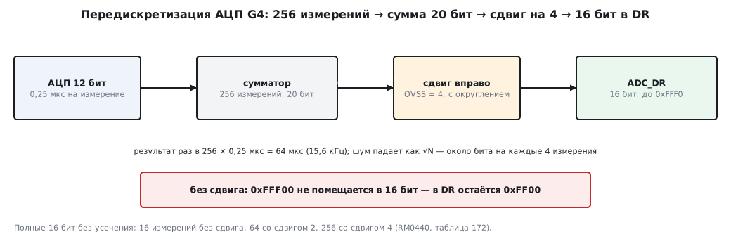
The ADC itself sums N conversions (from 2 to 256, the OVSR field), shifts
the sum right by M bits (0–8, the OVSS field) with rounding and puts it in DR.
The data register is 16 bits, and if the sum after the shift is longer, the top bits
are lost. The largest result for code 0xFFF (RM0440, table 172; the calculation
matched it in all 80 cells):
| N | Sum | Shift 0 | 2 | 4 | 8 |
|---|---|---|---|---|---|
| 16 | 0xFFF0 | 0xFFF0 | 0x3FFC | 0x0FFF | 0x0100 |
| 64 | 0x3FFC0 | 0xFFC0 (truncated) | 0xFFF0 | 0x3FFC | 0x0400 |
| 256 | 0xFFF00 | 0xFF00 (truncated) | 0xFFC0 (truncated) | 0xFFF0 | 0x0FFF |
Three combinations give the full 16 bits without truncation: 16 conversions without a shift, 64 with a shift of 2 and 256 with a shift of 4 — 0xFFF0 in every case. 256 conversions of 0.25 µs give a result every 64 µs, 15.6 kHz; 16 conversions every 4 µs, 250 kHz.
void adc_oversample_16bit(void)
{
    ADC1->CFGR2 = ADC_CFGR2_ROVSE | (OVSR_256 << ADC_CFGR2_OVSR_Pos) | (OVSS_4 << ADC_CFGR2_OVSS_Pos);
}
armclang turns it into a single write of 0x9D to address 0x5000 0010 — that is
ADC1->CFGR2.
How many bits the sum really gives depends on noise: summing identical codes is useless. A PC model — an ADC with noise of 1 code unit, random voltages:
| N | Shift | Residual noise, 12-bit units | Bits beyond 12 |
|---|---|---|---|
| 1 | 0 | 1.039 | 0.0 |
| 4 | 1 | 0.552 | 0.9 |
| 16 | 2 | 0.271 | 1.9 |
| 64 | 3 | 0.136 | 2.9 |
| 256 | 4 | 0.069 | 3.9 |
Every four conversions give about one bit: the noise falls as √N (section 165). 256 conversions give almost 4 bits — that is the 16 bits from a 12-bit ADC. If there is no noise, the extra bits are false: they are obtained by adding dither (section 165).
15а.6 Offset and gain correction
Offset: an OFRy register (there are four) is tied to a channel and subtracts
a given number from the result; the result becomes signed. Gain
correction: the code is multiplied by GCOMPCOEFF / 4096, from 0 to 3.999756
(RM0440); 0x1000 is exactly 1. A factor of 0x1040 (1.01562) turns
code 3000 into about 3047, 0x0FC0 (0.98438) into 2953. This corrects
the factory spread of an input divider without spending the processor on it. The correction is enabled
by the GCOMP bit in the same register as oversampling; writing
the whole register, as in the listing below, clears this bit.
Offset does not work with oversampling: with oversampling
enabled the OFFSETy_EN bits are ignored (RM0440).
15а.7 Pitfalls
- The ADC is silent after reset.
DEEPPWDwas not cleared orADVREGENwas not switched on with a 20 µs wait: calibration will not finish. - One calibration for two kinds of input. A differential channel
with single-ended calibration measures with an offset. Calibrate twice
(
ADCALDIF= 0 and 1). - HCLK / 1 at 170 MHz. A synchronous clock without a divider on the G474 gives 170 MHz to the ADC against a limit of 60. Use HCLK / 4 or an asynchronous clock from the PLL.
- A shift smaller than needed. 256 conversions without a shift give a sum of 0xFFF00, and
DRholds 0xFF00: the top 4 bits are lost, the result "floats" in strange ways. - Offset and oversampling together.
OFRyhas no effect with oversampling. DIFSELwith the ADC enabled. RM0440 allows writingDIFSELonly with the ADC disabled: differential mode is set beforeADEN.- The neighbouring channel of a differential pair in the sequence. Its pin is already taken by the negative input — it cannot be measured.
15а.8 Summary
- The G4 ADC: deep power-down and a regulator after reset, two calibrations, differential inputs, oversampling, offset and gain in the block.
- TCONV = sampling + 12.5 cycles: 0.25 µs at 60 MHz; on the G474 synchronously HCLK / 4 = 42.5 MHz, 0.353 µs.
- Differential code: 0x800 is zero, one unit is 1.611 mV at 3.3 V.
- Oversampling: the sum of N conversions with a shift of M; 16 bits without truncation — 16×0, 64×2, 256×4; every 4 conversions give about a bit, if there is noise.
- Gain correction: code ×
GCOMPCOEFF/ 4096; offset does not work with oversampling.
Full sources
adc15a.c — the STM32G474 ADC at register level: calibrations, a differential channel, oversampling.
/* 15а: АЦП STM32G474 по регистрам — две калибровки, дифференциальный канал, передискретизация 256x.
   Собирается armclang: -DSTM32G474xx. */
#include <stdint.h>

extern void wait_us(uint32_t us);

#define OVSR_256  7u                    /* CFGR2.OVSR: 000 — 2x … 111 — 256x */
#define OVSS_4    4u                    /* сдвиг на 4 бита: 12 + 8 − 4 = 16 бит */

_Static_assert(ADC_CFGR2_OVSR_Pos == 2 && ADC_CFGR2_OVSS_Pos == 5, "поля передискретизации в CFGR2");
_Static_assert(((OVSR_256 << ADC_CFGR2_OVSR_Pos) | (OVSS_4 << ADC_CFGR2_OVSS_Pos)) == 0x9Cu, "256x, сдвиг 4");

void adc_power_and_calibrate(void)
{
    RCC->AHB2ENR |= RCC_AHB2ENR_ADC12EN;
    ADC12_COMMON->CCR = 3u << ADC_CCR_CKMODE_Pos;   /* HCLK / 4: 170 / 4 = 42,5 МГц, не больше 60 */
    ADC1->CR &= ~ADC_CR_DEEPPWD;                    /* после сброса АЦП в глубоком сне */
    ADC1->CR |= ADC_CR_ADVREGEN;
    wait_us(20);                                    /* LL_ADC_DELAY_INTERNAL_REGUL_STAB_US */

    ADC1->CR &= ~ADC_CR_ADCALDIF;                   /* 1: несимметричные входы → CALFACT_S */
    ADC1->CR |= ADC_CR_ADCAL;
    while (ADC1->CR & ADC_CR_ADCAL) {
    }
    ADC1->CR |= ADC_CR_ADCALDIF;                    /* 2: дифференциальные → CALFACT_D */
    ADC1->CR |= ADC_CR_ADCAL;
    while (ADC1->CR & ADC_CR_ADCAL) {
    }
    ADC1->CR &= ~ADC_CR_ADCALDIF;

    ADC1->ISR = ADC_ISR_ADRDY;
    ADC1->CR |= ADC_CR_ADEN;
    while (!(ADC1->ISR & ADC_ISR_ADRDY)) {
    }
}

/* канал ch — дифференциальный: его отрицательный вход занимает другой канал (RM0440) */
void adc_differential(uint32_t ch)
{
    ADC1->DIFSEL |= 1u << ch;                       /* DIFSEL пишут при ADEN = 0 */
}

/* 16 бит из 256 измерений: 64 мкс на результат при 0,25 мкс на измерение */
void adc_oversample_16bit(void)
{
    ADC1->CFGR2 = ADC_CFGR2_ROVSE | (OVSR_256 << ADC_CFGR2_OVSR_Pos) | (OVSS_4 << ADC_CFGR2_OVSS_Pos);
}

uint16_t adc_read(uint32_t ch)
{
    ADC1->SQR1 = ch << ADC_SQR1_SQ1_Pos;            /* L = 0: одно измерение в очереди */
    ADC1->CR |= ADC_CR_ADSTART;
    while (!(ADC1->ISR & ADC_ISR_EOC)) {
    }
    return (uint16_t)ADC1->DR;
}
Next: section 15б "The external ADS1115 ADC over I2C: 16 bits, the PGA amplifier, the multiplexer, conversion modes and the ALERT/RDY pin" — when the built-in 12 bits are not enough: an external delta-sigma ADC on the I2C bus.