 Embedded HandbookApps
15б. The external ADS1115 ADC over I2C: 16 bits, the PGA amplifier, the multiplexer, conversion modes and the ALERT/RDY pin
Section 14 covers the built-in ADC of the F1 and F4: 12 bits, successive approximation, the supply as the reference. In 15а the G4 brought a differential input and 16 bits by oversampling, but the F103 has neither. When an F103 has to measure a shunt, a bridge or a thermocouple — a small signed difference, more precisely than 12 bits — an external ADC is added. The ADS1115 is the most common one: 16 bits, four inputs, an amplifier with a choice of range, I2C and a "ready" pin. Here: how it differs from the built-in one, how to connect it to the F103, which registers are needed, how to wait for the result, how to turn the code into microvolts, how much time one channel takes, how RDY and the comparator work and what to do about noise and mains hum.
Sources: RM0008 (DocID13902 Rev 17): the pin mode table, p. 160;
AFIO_EXTICR2, p. 190; EXTI_FTSR, p. 211; master reception of two
bytes, p. 764; I2C_CCR, p. 783–784; I2C_TRISE, p. 784. DocID13587 Rev 17
(STM32F103x8/xB): PB6 is I2C1_SCL, PB7 is I2C1_SDA, both FT, PB5 not FT,
p. 32. The project has no document on the ADS1115: the registers, the
Config bits, the codes and ranges, the data rates, the addresses, the
power-up values and the behaviour of OS and ALERT/RDY are taken from
the manufacturer's documentation and built into the model. So everything
below checks that the driver agrees with the model, not with the chip.
All numbers come from a run of the driver _verify/ads15c/ads15c.c on a
computer (gcc 12.2.0) with our own model of the ADS1115 as an I2C slave in
Python 3.11; the firmware is built by armclang 6.24 for the Cortex-M3.
What it is called in the documentation
Original Meaning delta-sigma ADC many coarse measurements plus a digital filter programmable gain amplifier (PGA) amplifier with a programmable gain — here, the choice of range full-scale range (FSR) the range: from −FS to +FS input multiplexer (MUX) input selector single-ended / differential input input against ground / difference of two inputs single-shot / continuous-conversion mode one conversion / back-to-back conversions operational status (OS) "start" bit on write and "converting" bit on read data rate (DR), SPS speed: conversions per second address pointer register pointer register: which register the exchange is with conversion ready (RDY) the result is ready comparator queue (COMP_QUE) how many conversions in a row before it trips window / latching comparator window comparator / comparator with a latch two's complement signed binary code
15б.1 How it differs from the built-in ADC
The F1 built-in ADC uses successive approximation: a short sample onto a capacitor (180.1) and 12 steps to find the code, 1.17 µs per measurement at 12 MHz (14.2). According to the manufacturer's documentation the ADS1115 works differently: a delta-sigma modulator measures the input coarsely during the whole conversion, and a digital filter turns those measurements into a 16-bit code. Everything else follows from this:
| F1 built-in ADC | ADS1115 | |
|---|---|---|
| resolution | 12 bits, positive only | 16 bits, signed |
| principle | successive approximation | delta-sigma with a filter |
| time per result | 1.17 µs at 12 MHz | 1/DR: from 125 ms to 1162.8 µs |
| input | from 0 to VREF+ | difference of two inputs or input against GND |
| range | 0…VREF+, set by the supply | from ±6.144 to ±0.256 V, set by the PGA |
| link | MCU bus, DMA | I2C, two bytes per result |
The built-in one is a thousand times faster and suits waveform capture. The external one is slow, but it averages the input over the conversion time by itself (in the model the filter is exactly such an average), measures a signed difference and on the ±0.256 V range gives a code step of 7.8125 µV — just right for a shunt or a bridge. It has no adjustable sampling time: the data rate DR takes care of that.
The code is two's complement, 32768 steps per half of the range. An input against GND uses only the positive half — that is 15 bits, not 16.
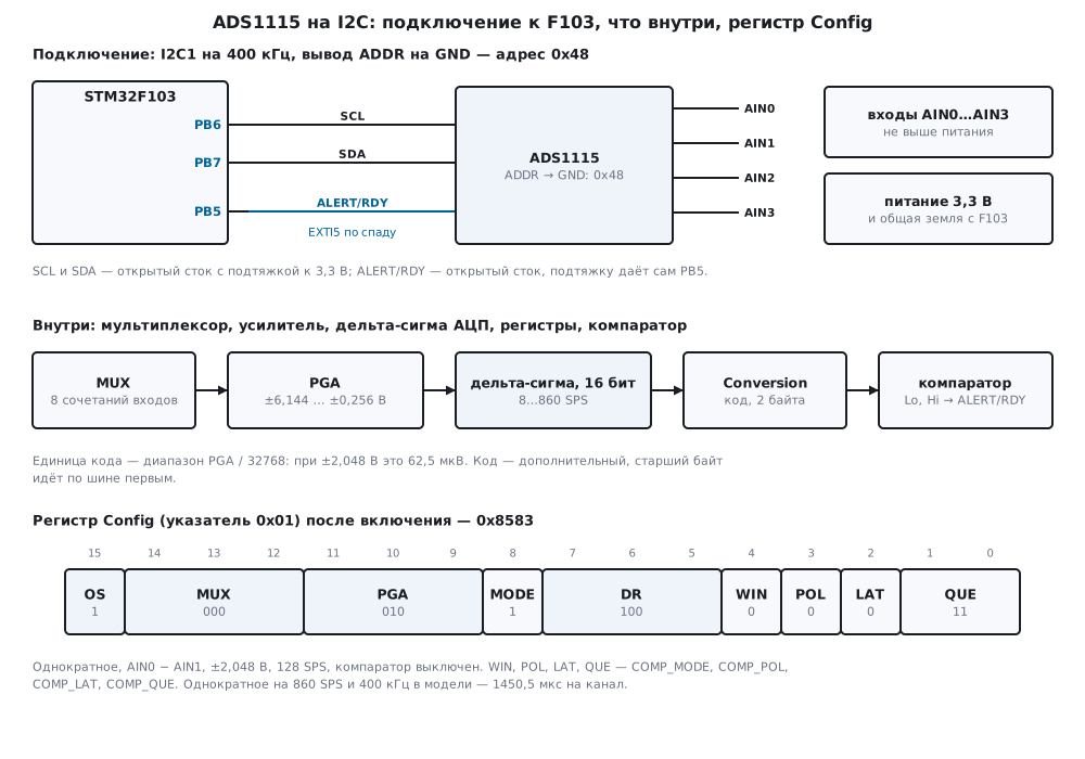
15б.2 Connecting it to the F103
| ADS1115 pin | STM32F103 | Purpose |
|---|---|---|
| SCL | PB6 | I2C1 clock |
| SDA | PB7 | I2C1 data |
| ALERT/RDY | PB5 | "ready" or threshold; EXTI5 on the falling edge |
| ADDR | GND | address 0x48 |
| VDD, GND | 3.3 V and ground | ground shared with the microcontroller |
PB6 and PB7 are I2C1 pins, both FT, that is, they tolerate 5 V (DocID13587,
p. 32): a module powered from 5 V with its own pull-ups to 5 V will not
burn them. PB5 is not FT. According to the manufacturer's documentation
ALERT/RDY is an open drain; the pull-up comes from PB5 itself, an input
with pull-up (code 1000 in the
mode table, p. 160), and it must not be pulled up to 5 V. The simplest is to power
the ADS1115 from 3.3 V — then the inputs cannot go above the supply (15б.7).
The ADDR pin sets the address (manufacturer's documentation): on GND —
0x48, on VDD — 0x49, on SDA — 0x4A, on SCL — 0x4B. So four chips, 16 inputs,
share one bus. In the model, for each of the four
connections ads_probe found one address, and the other three answered
with a refusal — ADS_E_NACK. On the wire, address 0x48 is the bytes 0x90 and 0x91
(17.2).
I2C1 is set up as in 17.3, but at 400 kHz, which the ADS1115 supports according to its documentation.
In fast mode with DUTY = 0 the low level of SCL is 2 × CCR and the
high level CCR APB1 clocks (p. 784): 36 MHz / (3 × 30) = 400 kHz.
TRISE is the maximum rise time plus one: 300 ns × 36 MHz = 10.8, and if it is not
an integer, the integer part is taken (p. 784) — 11:
static void i2c1_init(void)
{
    RCC->APB2ENR |= RCC_APB2ENR_IOPBEN | RCC_APB2ENR_AFIOEN;
    RCC->APB1ENR |= RCC_APB1ENR_I2C1EN;
    /* PB6, PB7 — альтернативная функция, открытый сток, 50 МГц (1111); PB5 — вход с подтяжкой (1000) */
    GPIOB->CRL = (GPIOB->CRL & 0x000FFFFFu) | 0xFF800000u;
    GPIOB->BSRR = 1u << 5;
    I2C1->CR1 = 0;                                      /* настраивать при PE = 0 */
    I2C1->CR2 = APB1_MHZ;
    I2C1->CCR = I2C_CCR_FS | 30u;                       /* DUTY = 0: 36 МГц / (3 × 30) = 400 кГц */
    I2C1->TRISE = APB1_MHZ * 300u / 1000u + 1u;         /* 300 нс × 36 МГц = 10,8 → 10 + 1 = 11 */
    I2C1->CR1 = I2C_CR1_PE;
}
RM0008 (p. 783) notes that to get exactly 400 kHz the APB1 frequency
must be a multiple of 10 MHz, and the real frequency may differ because of
the input filter. In the model the bus runs at exactly 400 kHz. ALERT/RDY goes to
EXTI5: AFIO_EXTICR2, bits 7:4 = 0001 — port B (p. 190), and the falling edge is enabled by
EXTI_FTSR (p. 211).
15б.3 Registers: the pointer, Conversion, Config, the thresholds
There are four registers of 16 bits each, plus the pointer register. The first byte of any
write goes into the pointer and selects the register: 0 — Conversion
(the result, read only), 1 — Config, 2 — Lo_thresh, 3 —
Hi_thresh. A write of three bytes is the pointer, then the high and low byte of the
value. A read returns two bytes of the register under the pointer, high byte
first, and leaves the pointer unchanged.
The first exchange in the model after power-up is ads_probe, a read of Config:
the bytes 90 01, a repeated start, 91 — and the answer 85 83. After
power-up Config = 0x8583, Lo_thresh = 0x8000, Hi_thresh = 0x7FFF,
Conversion = 0x0000.
| Bits | Field | What it sets | After power-up |
|---|---|---|---|
| 15 | OS |
write 1 — start a single-shot conversion; read 0 — converting | 1 |
| 14:12 | MUX |
000 — AIN0 − AIN1, 001 — AIN0 − AIN3, 010 — AIN1 − AIN3, 011 — AIN2 − AIN3, 100…111 — AIN0…AIN3 against GND | 000 |
| 11:9 | PGA |
000 — ±6.144 V, 001 — ±4.096, 010 — ±2.048, 011 — ±1.024, 100 — ±0.512, 101…111 — ±0.256 | 010 |
| 8 | MODE |
1 — single-shot, 0 — continuous | 1 |
| 7:5 | DR |
000…111 — 8, 16, 32, 64, 128, 250, 475, 860 SPS | 100 |
| 4 | COMP_MODE |
0 — comparator with hysteresis, 1 — window | 0 |
| 3 | COMP_POL |
0 — ALERT active low |
0 |
| 2 | COMP_LAT |
1 — hold ALERT until the result is read |
0 |
| 1:0 | COMP_QUE |
00, 01, 10 — trip after 1, 2, 4 conversions; 11 — off | 11 |
The driver's register read remembers where the pointer is: if it already points there, the extra byte is not needed.
int ads_read(ads_t *d, uint8_t reg, uint16_t *v)
{
uint8_t b[2];
int rc = d->ptr == reg ? xfer(d, 0, 0, b, 2) /* указатель уже на месте: только чтение */
: xfer(d, ®, 1, b, 2); /* иначе запись указателя и повторный старт */
if (rc == ADS_OK) {
d->ptr = reg;
*v = (uint16_t)(b[0] << 8 | b[1]);
}
return rc;
}
An exchange with a pointer write and a repeated start takes 48 SCL clocks, 120 µs
at 400 kHz; a read without the pointer — 29 clocks, 72.5 µs; a write of Config
— 38 clocks, 95 µs. For "single-shot, AIN0, ±4.096 V, 128 SPS" the driver
wrote 0xC383 into Config — the model built the same number from the fields of
the table independently; all four checked combinations matched.
15б.4 Single-shot and continuous, four channels in turn
Single-shot (MODE = 1): writing Config with OS = 1 starts one
conversion, after which the chip goes to sleep. The end is found from OS
(read 1 — done) or from the RDY pin (15б.6). Polling OS right away
is pointless: the result comes no earlier than after 1/DR. The driver first
waits that long, then polls every 100 µs:
/* однократное: OS = 1 запускает; сначала ждём расчётное время, потом опрашиваем OS */
int ads_single(ads_t *d, uint32_t mux, uint32_t pga, uint32_t dr, int16_t *code)
{
    uint16_t c;
    uint32_t t = ads_conv_us(dr);
    int rc = ads_write(d, ADS_CONFIG, ads_cfg(mux, pga, dr, 1) | ADS_QUE_OFF);
    if (rc)
        return rc;
    ads_port_delay_us(t);
    for (uint32_t waited = t;; waited += ADS_POLL_US) {
        if ((rc = ads_read(d, ADS_CONFIG, &c)) != ADS_OK)
            return rc;
        d->polls++;
        if (c & ADS_OS)                                 /* 1 — преобразование закончено */
            break;
        if (waited > 2u * t + 10000u)
            return ADS_E_TIMEOUT;
        ads_port_delay_us(ADS_POLL_US);
    }
    return ads_read_conv(d, code);
}
In the model at 400 kHz, input 1 V, ±2.048 V — code 16000 at every data rate:
| DR | 1/DR | OS after a pause |
exchanges | OS without a pause, polls |
by RDY |
exchanges |
|---|---|---|---|---|---|---|
| 8 SPS | 125 000 µs | 125 287.5 µs | 3 | 1726 | 125 212.5 µs | 2 |
| 128 SPS | 7812.5 µs | 8100.5 µs | 3 | 109 | 8025 µs | 2 |
| 250 SPS | 4000 µs | 4287.5 µs | 3 | 57 | 4212.5 µs | 2 |
| 860 SPS | 1162.8 µs | 1450.5 µs | 3 | 18 | 1375.3 µs | 2 |
1450.5 µs at 860 SPS is 95 µs to write Config, a 1163 µs pause,
72.5 µs to read Config and 120 µs to read the result with a pointer
write. Polling without a pause at 8 SPS is 1726 reads in a row: the bus is busy
for the whole conversion, and there is no room for other devices on it.
Continuous (MODE = 0): conversions run one after another,
Conversion always holds the latest. This is for one channel. Change the
input and the register still holds the old result: in the model, continuous conversion on AIN0
(code 4000) was switched to AIN3 and read at once — 4000; after the
next RDY — 16000. In the model a write of Config restarts the
conversion; whether the chip does the same was not checked — it is safer to
throw away the first result after an input change.
Four channels in turn are easier with single-shot conversions: each one starts with the new input already selected.
/* четыре несимметричных входа по очереди, каждый — однократным преобразованием */
int ads_scan4(ads_t *d, uint32_t pga, uint32_t dr, int16_t out[4])
{
    for (uint32_t ch = 0; ch < 4u; ch++) {
        int rc = ads_single(d, ADS_AIN0 + ch, pga, dr, &out[ch]);
        if (rc != ADS_OK && rc != ADS_E_OVER)
            return rc;
    }
    return ADS_OK;
}
Inputs of 0.5, 1.0, 1.5 and 2.0 V on ±4.096 V give codes 4000, 8000, 12000 and 16000, 12 exchanges and 4 polls per round. Time per channel:
| DR | 1/DR | per channel, 100 kHz | per channel, 400 kHz |
|---|---|---|---|
| 8 SPS | 125 000 µs | 126 150 µs | 125 287.5 µs |
| 128 SPS | 7812.5 µs | 8963 µs | 8100.5 µs |
| 250 SPS | 4000 µs | 5150 µs | 4287.5 µs |
| 475 SPS | 2105.3 µs | 3256 µs | 2393.5 µs |
| 860 SPS | 1162.8 µs | 2313 µs | 1450.5 µs |
The bus adds 287.7 µs to a conversion at 400 kHz and 1150.2 µs at 100 kHz: at 860 SPS and 100 kHz a channel takes almost twice as long as the conversion itself. All four inputs at 860 SPS and 400 kHz take 5802 µs.
15б.5 Code to microvolts, sign, noise and data rate
One code step is the PGA range / 32768. Integer conversion: code × FS in microvolts / 32768 with rounding. The product does not fit in 32 bits (32767 × 6 144 000), so it is 64-bit, and the division by 32768 is a shift:
/* код → микровольты целыми: код × FS / 32768 с округлением, без деления */
int32_t ads_uv(int16_t code, uint32_t pga)
{
    int64_t x = (int64_t)code * fs_mv[pga > 5u ? 5u : pga] * 1000;    /* PGA 110 и 111 — тоже ±0,256 В */
    return (int32_t)(x >= 0 ? (x + 16384) >> 15 : -((-x + 16384) >> 15));
}
armclang built ads_uv into 84 bytes: SMULL and UMULL multiplications, no
library calls. In the model, input against GND:
| PGA | Code step | 0.2 V: code | back, µV | 1.0 V: code |
|---|---|---|---|---|
| ±6.144 V | 187.5 µV | 1067 | 200 063 | 5333 |
| ±4.096 V | 125 µV | 1600 | 200 000 | 8000 |
| ±2.048 V | 62.5 µV | 3200 | 200 000 | 16000 |
| ±1.024 V | 31.25 µV | 6400 | 200 000 | 32000 |
| ±0.512 V | 15.625 µV | 12800 | 200 000 | 32767 — the limit |
| ±0.256 V | 7.8125 µV | 25600 | 200 000 | 32767 — the limit |
The extreme values: ads_uv(32767, ±6.144 V) = 6 143 813 µV,
ads_uv(−32768, ±2.048 V) = −2 048 000 µV, one step on ±0.256 V is
8 µV after rounding.
Sign. The code is int16_t, not uint16_t. A difference AIN0 − AIN1 =
1.25 − 1.00 V on ±2.048 V gives code 4000 (0x0FA0), 250 000 µV; with the inputs
swapped — −4000 (0xF060), −250 000 µV. And an input against GND can be
negative too: −2 mV on AIN0 gave −32 (0xFFE0), −2000 µV. Read
as uint16_t, this code would become 65504.
Noise. In the model the chip noise is set to 2 µV × √DR (rms) — an assumption, not data from a document. 400 results each on a difference of 100 mV:
| DR | Model noise | ±0.256 V: rms, codes | distinct codes | ±2.048 V: rms, codes | distinct codes | ±0.256 V, mean of 16 |
|---|---|---|---|---|---|---|
| 8 SPS | 5.66 µV | 0.78 | 5 | 0 | 1 | 1.62 µV |
| 128 SPS | 22.63 µV | 2.91 | 15 | 0.43 | 3 | 5.2 µV |
| 860 SPS | 58.65 µV | 7.56 | 40 | 1.01 | 7 | 12.16 µV |
On ±2.048 V at 8 SPS all 400 results are equal: the noise is smaller than one code step, and there is nothing to average (14а.6, 165.8). On ±0.256 V the noise is several codes, and the mean of 16 cuts it roughly fourfold. A narrow PGA range and a slow data rate are the first things that give precision.
Mains hum. The averaging filter over 1/DR suppresses a sine the more, the more of its periods fit into one conversion. A 50 Hz hum of 1 mV amplitude in the difference, 64 results:
| DR | 50 Hz periods per conversion | Hum left |
|---|---|---|
| 8 SPS | 6.25 | 31.2 µV |
| 16 SPS | 3.125 | 39.1 µV |
| 32 SPS | 1.5625 | 195.3 µV |
| 64 SPS | 0.7812 | 257.8 µV |
| 128 SPS | 0.3906 | 765.6 µV |
| 250 SPS | 0.2 | 929.7 µV |
| 475 SPS | 0.1053 | 984.4 µV |
| 860 SPS | 0.0581 | 992.2 µV |
No data rate gives zero: none of them is a divisor of 50 Hz. Zero
comes from the mean of consecutive results spanning exactly 20 ms: at 250 SPS
ads_average of 5 leaves 1.6 µV, at 860 SPS of 17 (19.767 ms) —
12.4 µV, at 128 SPS of 3 (23.438 ms) — 140.6 µV. But the trick relies on an
exact conversion rate: in the model with the rate 3 % lower (a window of
20.6 ms) 29.7 µV is left at 250 SPS. How far the chip's rate is from
nominal was not checked.
15б.6 ALERT/RDY: "ready" and the comparator
The ALERT/RDY pin has two jobs. "Ready" is enabled by a special
combination of thresholds (manufacturer's documentation): the top bit of
Hi_thresh = 1, the top bit of Lo_thresh = 0, and COMP_QUE ≠ 11:
/* ALERT/RDY как «готово»: старший бит Hi_thresh = 1, старший бит Lo_thresh = 0, COMP_QUE ≠ 11 */
int ads_rdy_mode(ads_t *d)
{
    int rc = ads_write(d, ADS_HI_THRESH, 0x8000u);
    return rc ? rc : ads_write(d, ADS_LO_THRESH, 0x0000u);
}

int ads_single_rdy(ads_t *d, uint32_t mux, uint32_t pga, uint32_t dr, int16_t *code)
{
    uint32_t t = ads_conv_us(dr);
    (void)ads_port_wait_rdy(0);                         /* снять старый флаг EXTI */
    int rc = ads_write(d, ADS_CONFIG, ads_cfg(mux, pga, dr, 1) | ADS_QUE_1);
    if (rc)
        return rc;
    if (!ads_port_wait_rdy(2u * t + 10000u))
        return ADS_E_TIMEOUT;
    return ads_read_conv(d, code);
}
In the firmware a falling edge on PB5 sets a flag in the interrupt, and the port waits for it with a timeout:
/* ALERT/RDY: спад на PB5 */
void EXTI9_5_IRQHandler(void)
{
    EXTI->PR = 1u << 5;
    rdy = 1;
}

int ads_port_wait_rdy(uint32_t timeout_us)
{
    uint32_t t0 = DWT->CYCCNT;
    while (!rdy) {
        if (expired(t0, timeout_us))
            return 0;
    }
    rdy = 0;
    return 1;
}
Single-shot by RDY takes 2 exchanges instead of 3, at 860 SPS 1375.3 µs instead of
1450.5 (15б.4), and the bus is free in between. In continuous mode RDY
is a short pulse at the end of each conversion: in the model
ads_average at 860 SPS collected 860 results in 1 000 070 µs, one
falling edge and one exchange per result, the mean is code 16000.
Two mistakes keep RDY silent: COMP_QUE = 11 (comparator
off, pin released) or thresholds left at their power-up values —
then it is an ordinary comparator with a threshold of 0x7FFF. In the model in both cases
10 conversions passed with 0 falling edges, and ads_average returned
ADS_E_TIMEOUT after 12 326 µs.
Comparator. With ordinary thresholds ALERT watches the level by itself, without
polling. With hysteresis (COMP_MODE = 0) it trips when the code is above
Hi_thresh and releases when it is below Lo_thresh; the window (COMP_MODE = 1)
trips when the code is outside the interval. COMP_QUE requires 1, 2 or 4 conversions
in a row, COMP_LAT holds the trip until the result is read. In the model
the input swings slowly from 1.35 to 1.55 V (a 0.5 Hz sine) with sensor noise
of 5 mV, 128 SPS, ±2.048 V, 10 s — 1280 conversions and five rises
through 1.5 V:
| Setting | Lo_thresh |
Hi_thresh |
ALERT falling edges |
|---|---|---|---|
| no hysteresis, both thresholds 1.50 V | 24000 | 24000 | 14 |
| hysteresis 1.40–1.50 V | 22400 | 24000 | 5 |
no hysteresis, COMP_QUE — 4 in a row |
24000 | 24000 | 5 |
| window 1.40–1.50 V | 22400 | 24000 | 25 |
| hysteresis and latch | 22400 | 24000 | 1 |
Without hysteresis the noise near the threshold gives extra trips — 14 for five rises. Hysteresis or a queue of four leave exactly five. With the latch the pin tripped once and stayed low: nobody read the result.
15б.7 Pitfalls
Input beyond the supply. According to the manufacturer's documentation the voltage on the inputs must stay from GND − 0.3 V to VDD + 0.3 V, and the ±6.144 V range does not cancel that. With a 3.3 V supply the model flagged a violation at 5 V, but not at 3.3 and 3.6 V; a 3.3 V input on ±6.144 V gives code 17600 out of 32767. What the real chip does with 5 V was not checked — use a divider or power the ADS1115 from 5 V.
±0.256 V on a large signal. The code hits 32767, and that looks like a
real number. In the model 1 V on ±0.256 V gives 32767, and ads_read_conv
returned ADS_E_OVER. The driver must tell the range limit from a
measurement.
The bus hangs. The microcontroller was reset in the middle of a read while the
ADS1115 was sending a zero — it holds SDA and waits for clocks (17.6). In the model, out of
1000 random resets 508 left SDA low. Until the bus is
freed, every exchange ends with ADS_E_BUS on the port timeout
(1000 µs). The nine SCL clocks from 17.6 freed all 508, no more than
7 clocks were needed, and the next measurement succeeded in all 508.
Byte order mixed up. The ADS1115 sends the high byte first, while the F103 —
like a PC — stores the low byte first. The bytes 0F A0, copied into
int16_t as they are, gave −24561 instead of 4000; F0 60 — 24816 instead of
−4000. Assemble with a shift, as ads_be16 does.
Changed the input in continuous mode and read at once. The old input is read: 4000 instead of 16000 (15б.4).
RDY is silent. COMP_QUE = 11 or the thresholds were not changed — 0 falling edges,
a timeout after 12 326 µs (15б.6).
The device does not answer. The ADDR pin is wired elsewhere — 0x48 gives
ADS_E_NACK. Or the driver was given the shifted address 0x90 instead of 0x48
(17.2).
15б.8 Summary
- The ADS1115 is delta-sigma, 16 bits signed, 8–860 SPS, PGA from ±6.144 to ±0.256 V, four inputs or two differences, I2C; the F1 built-in ADC takes 1.17 µs, the external one 1162.8 µs and more, but it averages by itself.
- F103: I2C1 on PB6 and PB7 (FT), 400 kHz —
CCR=F/S| 30,TRISE= 11;ALERT/RDYon PB5 with pull-up on EXTI5;ADDRon GND — 0x48. - The pointer register selects the register;
Configafter power-up is 0x8583; a read with the same pointer takes 72.5 µs instead of 120 µs. - Single-shot: a 1/DR pause, then
OS— 1450.5 µs per channel at 860 SPS and 400 kHz, 2313 µs at 100 kHz; byRDY— 1375.3 µs and 2 exchanges. - Code × FS / 32768 in integers,
int16_t; 7.8125 µV on ±0.256 V; at ±2.048 V and 8 SPS the noise is below one step and averaging gives nothing. - No data rate suppresses 50 Hz; a mean of 5 at 250 SPS over 20 ms leaves 1.6 µV out of 1000.
RDY: top bit ofHi_thresh1, ofLo_thresh0,COMP_QUE≠ 11; give the comparator hysteresis: 5 trips instead of 14.
Full sources
ads15c.h — registers, Config bits, MUX, PGA and DR codes, the port and the driver functions.
/* ads15c.h — раздел 15б: драйвер внешнего АЦП ADS1115 по I2C без регистров микроконтроллера.
 * Драйвер говорит с микросхемой только через три функции порта (ads_port_*): в прошивке fw15c.c их
 * делают I2C1 и EXTI5 STM32F103, в стенде host15c.c — модель model15c.py.
 * Карта регистров, биты Config, коды PGA, скорости и адреса — по документации производителя;
 * документа в проекте нет, с микросхемой не сверено. */
#ifndef ADS15C_H
#define ADS15C_H
#include <stdint.h>

/* ── регистры: номер пишется первым байтом записи в регистр указателя ── */
#define ADS_CONV          0x00u         /* результат, 16 бит, дополнительный код; только чтение */
#define ADS_CONFIG        0x01u
#define ADS_LO_THRESH     0x02u
#define ADS_HI_THRESH     0x03u

/* ── Config ───────────────────────────────────────────────────────────── */
#define ADS_OS            0x8000u       /* запись 1 — начать однократное; чтение 0 — идёт преобразование */
#define ADS_MUX_POS       12u           /* 14:12 — вход */
#define ADS_PGA_POS       9u            /* 11:9 — диапазон */
#define ADS_MODE_SINGLE   0x0100u       /* 1 — однократное с засыпанием, 0 — непрерывное */
#define ADS_DR_POS        5u            /* 7:5 — скорость */
#define ADS_COMP_WINDOW   0x0010u       /* компаратор: 0 — с гистерезисом, 1 — окно */
#define ADS_COMP_POL_HIGH 0x0008u       /* 0 — ALERT активен нулём */
#define ADS_COMP_LAT      0x0004u       /* 1 — держать ALERT до чтения результата */
#define ADS_QUE_1         0x0000u       /* COMP_QUE 1:0: сработать после 1, 2 или 4 преобразований */
#define ADS_QUE_2         0x0001u
#define ADS_QUE_4         0x0002u
#define ADS_QUE_OFF       0x0003u       /* компаратор выключен, ALERT отпущен */
#define ADS_CONFIG_RESET  0x8583u       /* после включения питания */

enum { ADS_AIN0_AIN1, ADS_AIN0_AIN3, ADS_AIN1_AIN3, ADS_AIN2_AIN3,     /* MUX 000…011 — разность */
       ADS_AIN0, ADS_AIN1, ADS_AIN2, ADS_AIN3 };                        /* MUX 100…111 — против GND */
enum { ADS_FS_6144, ADS_FS_4096, ADS_FS_2048, ADS_FS_1024, ADS_FS_512, ADS_FS_256 };   /* PGA 000…101 */
enum { ADS_DR_8, ADS_DR_16, ADS_DR_32, ADS_DR_64, ADS_DR_128, ADS_DR_250, ADS_DR_475, ADS_DR_860 };

#define ADS_ADDR_GND      0x48u         /* вывод ADDR на GND; на VDD — 0x49, на SDA — 0x4A, на SCL — 0x4B */
#define ADS_POLL_US       100u          /* шаг опроса OS после расчётного времени */

enum { ADS_OK = 0, ADS_E_NACK = -1, ADS_E_BUS = -2, ADS_E_TIMEOUT = -3, ADS_E_OVER = -4 };

typedef struct {
    uint8_t addr;                       /* семибитный адрес: 0x48…0x4B */
    uint8_t ptr;                        /* что сейчас в регистре указателя; 0xFF — неизвестно */
    uint16_t cfg;                       /* последнее, что драйвер записал в Config */
    uint32_t xfers, polls, errors;      /* обменов по I2C, опросов OS, ошибок шины */
} ads_t;

/* ── порт: в прошивке — I2C1 и EXTI5, в стенде — строки к модели ─────── */
/* записать ntx байт; если nrx > 0 — повторный старт и прочитать nrx байт; 0, ADS_E_NACK или ADS_E_BUS */
int ads_port_xfer(uint8_t addr7, const uint8_t *tx, uint32_t ntx, uint8_t *rx, uint32_t nrx);
void ads_port_delay_us(uint32_t us);
/* ждать спада на ALERT/RDY (флаг EXTI) не дольше timeout_us; 1 — был, флаг снят; 0 — не было */
int ads_port_wait_rdy(uint32_t timeout_us);
/* девять тактов SCL вручную и STOP (раздел 17.6): число тактов до отпускания SDA или −1 */
int ads_port_bus_recover(void);

/* ── драйвер ──────────────────────────────────────────────────────────── */
uint16_t ads_cfg(uint32_t mux, uint32_t pga, uint32_t dr, int single);
int ads_probe(ads_t *d, uint8_t addr7);
int ads_write(ads_t *d, uint8_t reg, uint16_t v);
int ads_read(ads_t *d, uint8_t reg, uint16_t *v);
uint32_t ads_conv_us(uint32_t dr);
int ads_single(ads_t *d, uint32_t mux, uint32_t pga, uint32_t dr, int16_t *code);
int ads_rdy_mode(ads_t *d);
int ads_single_rdy(ads_t *d, uint32_t mux, uint32_t pga, uint32_t dr, int16_t *code);
int ads_continuous(ads_t *d, uint32_t mux, uint32_t pga, uint32_t dr, uint16_t comp);
int ads_read_conv(ads_t *d, int16_t *code);
int ads_average(ads_t *d, uint32_t n, int32_t *sum);
int ads_scan4(ads_t *d, uint32_t pga, uint32_t dr, int16_t out[4]);
int ads_thresholds(ads_t *d, int16_t lo, int16_t hi);
int ads_recover(ads_t *d);
int32_t ads_uv(int16_t code, uint32_t pga);
int16_t ads_be16(const uint8_t b[2]);

#endif
ads15c.c — driver: pointer, single-shot and continuous, RDY, four channels, microvolts.
/* ads15c.c — раздел 15б: драйвер ADS1115 по I2C. Один и тот же файл собирается в прошивку (armclang,
* Cortex-M3) и в стенд на компьютере (gcc): микроконтроллера он не знает, только порт ads_port_*. */
#include "ads15c.h"
static const uint16_t fs_mv[6] = {6144, 4096, 2048, 1024, 512, 256}; /* PGA 000…101 */
static const uint16_t sps[8] = {8, 16, 32, 64, 128, 250, 475, 860}; /* DR 000…111 */
uint16_t ads_cfg(uint32_t mux, uint32_t pga, uint32_t dr, int single)
{
uint32_t c = (mux & 7u) << ADS_MUX_POS | (pga & 7u) << ADS_PGA_POS | (dr & 7u) << ADS_DR_POS;
return (uint16_t)(single ? c | ADS_OS | ADS_MODE_SINGLE : c);
}
static int xfer(ads_t *d, const uint8_t *tx, uint32_t ntx, uint8_t *rx, uint32_t nrx)
{
int rc = ads_port_xfer(d->addr, tx, ntx, rx, nrx);
d->xfers++;
if (rc) {
d->errors++;
d->ptr = 0xFF; /* неизвестно, дошёл ли указатель */
}
return rc;
}
int ads_write(ads_t *d, uint8_t reg, uint16_t v)
{
uint8_t b[3] = {reg, (uint8_t)(v >> 8), (uint8_t)v}; /* старший байт первым */
int rc = xfer(d, b, 3, 0, 0);
if (rc == ADS_OK) {
d->ptr = reg;
if (reg == ADS_CONFIG)
d->cfg = v;
}
return rc;
}
int ads_read(ads_t *d, uint8_t reg, uint16_t *v)
{
uint8_t b[2];
int rc = d->ptr == reg ? xfer(d, 0, 0, b, 2) /* указатель уже на месте: только чтение */
: xfer(d, ®, 1, b, 2); /* иначе запись указателя и повторный старт */
if (rc == ADS_OK) {
d->ptr = reg;
*v = (uint16_t)(b[0] << 8 | b[1]);
}
return rc;
}
int16_t ads_be16(const uint8_t b[2])
{
return (int16_t)(uint16_t)(b[0] << 8 | b[1]);
}
int ads_probe(ads_t *d, uint8_t addr7)
{
uint16_t v;
d->addr = addr7;
d->ptr = 0xFF;
d->xfers = d->polls = d->errors = 0;
int rc = ads_read(d, ADS_CONFIG, &v); /* ответил ли кто-то по этому адресу */
if (rc == ADS_OK)
d->cfg = v;
return rc;
}
uint32_t ads_conv_us(uint32_t dr)
{
return (1000000u + sps[dr & 7u] - 1u) / sps[dr & 7u];
}
int ads_read_conv(ads_t *d, int16_t *code)
{
uint16_t v;
int rc = ads_read(d, ADS_CONV, &v);
if (rc)
return rc;
*code = (int16_t)v;
return v == 0x7FFFu || v == 0x8000u ? ADS_E_OVER : ADS_OK; /* упёрлись в край диапазона PGA */
}
/* однократное: OS = 1 запускает; сначала ждём расчётное время, потом опрашиваем OS */
int ads_single(ads_t *d, uint32_t mux, uint32_t pga, uint32_t dr, int16_t *code)
{
uint16_t c;
uint32_t t = ads_conv_us(dr);
int rc = ads_write(d, ADS_CONFIG, ads_cfg(mux, pga, dr, 1) | ADS_QUE_OFF);
if (rc)
return rc;
ads_port_delay_us(t);
for (uint32_t waited = t;; waited += ADS_POLL_US) {
if ((rc = ads_read(d, ADS_CONFIG, &c)) != ADS_OK)
return rc;
d->polls++;
if (c & ADS_OS) /* 1 — преобразование закончено */
break;
if (waited > 2u * t + 10000u)
return ADS_E_TIMEOUT;
ads_port_delay_us(ADS_POLL_US);
}
return ads_read_conv(d, code);
}
/* ALERT/RDY как «готово»: старший бит Hi_thresh = 1, старший бит Lo_thresh = 0, COMP_QUE ≠ 11 */
int ads_rdy_mode(ads_t *d)
{
int rc = ads_write(d, ADS_HI_THRESH, 0x8000u);
return rc ? rc : ads_write(d, ADS_LO_THRESH, 0x0000u);
}
int ads_single_rdy(ads_t *d, uint32_t mux, uint32_t pga, uint32_t dr, int16_t *code)
{
uint32_t t = ads_conv_us(dr);
(void)ads_port_wait_rdy(0); /* снять старый флаг EXTI */
int rc = ads_write(d, ADS_CONFIG, ads_cfg(mux, pga, dr, 1) | ADS_QUE_1);
if (rc)
return rc;
if (!ads_port_wait_rdy(2u * t + 10000u))
return ADS_E_TIMEOUT;
return ads_read_conv(d, code);
}
int ads_continuous(ads_t *d, uint32_t mux, uint32_t pga, uint32_t dr, uint16_t comp)
{
return ads_write(d, ADS_CONFIG, ads_cfg(mux, pga, dr, 0) | (comp & 0x1Fu));
}
/* n результатов подряд в непрерывном режиме по RDY; сумма — в *sum */
int ads_average(ads_t *d, uint32_t n, int32_t *sum)
{
uint32_t t = ads_conv_us(d->cfg >> ADS_DR_POS & 7u);
int16_t code;
*sum = 0;
(void)ads_port_wait_rdy(0);
for (uint32_t i = 0; i < n; i++) {
if (!ads_port_wait_rdy(2u * t + 10000u))
return ADS_E_TIMEOUT;
int rc = ads_read_conv(d, &code);
if (rc != ADS_OK && rc != ADS_E_OVER)
return rc;
*sum += code;
}
return ADS_OK;
}
/* четыре несимметричных входа по очереди, каждый — однократным преобразованием */
int ads_scan4(ads_t *d, uint32_t pga, uint32_t dr, int16_t out[4])
{
for (uint32_t ch = 0; ch < 4u; ch++) {
int rc = ads_single(d, ADS_AIN0 + ch, pga, dr, &out[ch]);
if (rc != ADS_OK && rc != ADS_E_OVER)
return rc;
}
return ADS_OK;
}
int ads_thresholds(ads_t *d, int16_t lo, int16_t hi)
{
int rc = ads_write(d, ADS_LO_THRESH, (uint16_t)lo);
return rc ? rc : ads_write(d, ADS_HI_THRESH, (uint16_t)hi);
}
int ads_recover(ads_t *d)
{
d->ptr = 0xFF;
return ads_port_bus_recover() < 0 ? ADS_E_BUS : ADS_OK;
}
/* код → микровольты целыми: код × FS / 32768 с округлением, без деления */
int32_t ads_uv(int16_t code, uint32_t pga)
{
int64_t x = (int64_t)code * fs_mv[pga > 5u ? 5u : pga] * 1000; /* PGA 110 и 111 — тоже ±0,256 В */
return (int32_t)(x >= 0 ? (x + 16384) >> 15 : -((-x + 16384) >> 15));
}
fw15c.c — STM32F103 firmware: I2C1 at 400 kHz, EXTI5 on ALERT/RDY, bus recovery.
/* fw15c.c — раздел 15б: ADS1115 на STM32F103 (BluePill), 72 МГц, APB1 = 36 МГц.
 * I2C1: PB6 — SCL, PB7 — SDA (открытый сток, 400 кГц); PB5 — ALERT/RDY (вход с подтяжкой, EXTI5 по спаду).
 * ADDR микросхемы — на GND: адрес 0x48. Раз в 100 мс — четыре входа по очереди (±4,096 В, 128 SPS) и
 * разность AIN0 − AIN1 по RDY (±2,048 В) в микровольтах. Тактирование до 72 МГц — как в разделе 6. */
#include "stm32f10x.h"
#include "ads15c.h"

#define CPU_HZ          72000000u
#define APB1_MHZ        36u
#define I2C_TIMEOUT_US  1000u           /* дольше любого флага на 400 кГц; столько ждёт и модель */

static ads_t adc;
static volatile uint8_t rdy;
volatile int32_t uv[5];                 /* AIN0…AIN3 и AIN0 − AIN1, мкВ */
volatile uint32_t bus_errors;

static int expired(uint32_t t0, uint32_t us)
{
    return DWT->CYCCNT - t0 >= us * (CPU_HZ / 1000000u);
}

void ads_port_delay_us(uint32_t us)
{
    uint32_t t0 = DWT->CYCCNT;
    while (!expired(t0, us)) {
    }
}

static void i2c1_init(void)
{
    RCC->APB2ENR |= RCC_APB2ENR_IOPBEN | RCC_APB2ENR_AFIOEN;
    RCC->APB1ENR |= RCC_APB1ENR_I2C1EN;
    /* PB6, PB7 — альтернативная функция, открытый сток, 50 МГц (1111); PB5 — вход с подтяжкой (1000) */
    GPIOB->CRL = (GPIOB->CRL & 0x000FFFFFu) | 0xFF800000u;
    GPIOB->BSRR = 1u << 5;
    I2C1->CR1 = 0;                                      /* настраивать при PE = 0 */
    I2C1->CR2 = APB1_MHZ;
    I2C1->CCR = I2C_CCR_FS | 30u;                       /* DUTY = 0: 36 МГц / (3 × 30) = 400 кГц */
    I2C1->TRISE = APB1_MHZ * 300u / 1000u + 1u;         /* 300 нс × 36 МГц = 10,8 → 10 + 1 = 11 */
    I2C1->CR1 = I2C_CR1_PE;
}

static int sr1_wait(uint16_t mask)
{
    uint32_t t0 = DWT->CYCCNT;
    while (!(I2C1->SR1 & mask)) {
        if (I2C1->SR1 & I2C_SR1_AF)
            return ADS_E_NACK;                          /* адрес или байт не подтверждён */
        if (expired(t0, I2C_TIMEOUT_US))
            return ADS_E_BUS;
    }
    return ADS_OK;
}

static int fail(int rc)
{
    I2C1->CR1 |= I2C_CR1_STOP;
    I2C1->SR1 = (uint16_t)~I2C_SR1_AF;                  /* AF снимается записью нуля */
    I2C1->CR1 &= (uint16_t)~(I2C_CR1_POS | I2C_CR1_ACK);
    return rc;
}

int ads_port_xfer(uint8_t addr7, const uint8_t *tx, uint32_t ntx, uint8_t *rx, uint32_t nrx)
{
    int rc;
    uint32_t t0 = DWT->CYCCNT;
    if (nrx != 0u && nrx != 2u)
        return ADS_E_BUS;                               /* драйвер читает только по два байта */
    while (I2C1->SR2 & I2C_SR2_BUSY) {                  /* SDA держит ведомый — раздел 17.6 */
        if (expired(t0, I2C_TIMEOUT_US))
            return ADS_E_BUS;
    }
    if (ntx) {
        I2C1->CR1 |= I2C_CR1_START;
        if ((rc = sr1_wait(I2C_SR1_SB)) != ADS_OK)
            return fail(rc);
        I2C1->DR = (uint8_t)(addr7 << 1);
        if ((rc = sr1_wait(I2C_SR1_ADDR)) != ADS_OK)
            return fail(rc);
        (void)I2C1->SR2;                                /* ADDR снят: SR1 прочитан в sr1_wait, теперь SR2 */
        for (uint32_t i = 0; i < ntx; i++) {
            if ((rc = sr1_wait(I2C_SR1_TXE)) != ADS_OK)
                return fail(rc);
            I2C1->DR = tx[i];
        }
        if ((rc = sr1_wait(I2C_SR1_BTF)) != ADS_OK)
            return fail(rc);
    }
    if (!nrx) {
        I2C1->CR1 |= I2C_CR1_STOP;
        return ADS_OK;
    }
    I2C1->CR1 |= I2C_CR1_START;                         /* после записи — повторный старт */
    if ((rc = sr1_wait(I2C_SR1_SB)) != ADS_OK)
        return fail(rc);
    I2C1->CR1 |= I2C_CR1_POS | I2C_CR1_ACK;             /* два байта: RM0008, с. 764 */
    I2C1->DR = (uint8_t)(addr7 << 1 | 1u);
    if ((rc = sr1_wait(I2C_SR1_ADDR)) != ADS_OK)
        return fail(rc);
    (void)I2C1->SR2;
    I2C1->CR1 &= (uint16_t)~I2C_CR1_ACK;
    if ((rc = sr1_wait(I2C_SR1_BTF)) != ADS_OK)         /* оба байта приняты, SCL прижат */
        return fail(rc);
    I2C1->CR1 |= I2C_CR1_STOP;
    rx[0] = (uint8_t)I2C1->DR;                          /* старший байт */
    rx[1] = (uint8_t)I2C1->DR;
    I2C1->CR1 &= (uint16_t)~I2C_CR1_POS;
    return ADS_OK;
}

/* ALERT/RDY: спад на PB5 */
void EXTI9_5_IRQHandler(void)
{
    EXTI->PR = 1u << 5;
    rdy = 1;
}

int ads_port_wait_rdy(uint32_t timeout_us)
{
    uint32_t t0 = DWT->CYCCNT;
    while (!rdy) {
        if (expired(t0, timeout_us))
            return 0;
    }
    rdy = 0;
    return 1;
}

/* то же, что в разделе 17.6, но возвращает число тактов */
int ads_port_bus_recover(void)
{
    int n = 0;
    I2C1->CR1 &= (uint16_t)~I2C_CR1_PE;
    GPIOB->BSRR = 1u << 6 | 1u << 7;
    GPIOB->CRL = (GPIOB->CRL & 0x00FFFFFFu) | 0x77000000u;    /* PB6, PB7 — выход, открытый сток (0111) */
    while (n < 9 && !(GPIOB->IDR & 1u << 7)) {         /* пока SDA в нуле */
        GPIOB->BRR = 1u << 6;
        ads_port_delay_us(5);
        GPIOB->BSRR = 1u << 6;
        ads_port_delay_us(5);
        n++;
    }
    int stuck = !(GPIOB->IDR & 1u << 7);
    GPIOB->BRR = 1u << 6;                               /* STOP: SDA вверх при высоком SCL */
    GPIOB->BRR = 1u << 7;
    ads_port_delay_us(5);
    GPIOB->BSRR = 1u << 6;
    ads_port_delay_us(5);
    GPIOB->BSRR = 1u << 7;
    ads_port_delay_us(5);
    I2C1->CR1 = I2C_CR1_SWRST;
    I2C1->CR1 = 0;
    i2c1_init();
    return stuck ? -1 : n;
}

static void irq_init(void)
{
    AFIO->EXTICR[1] = (AFIO->EXTICR[1] & ~0xF0u) | 0x10u;    /* EXTI5 ← PB5 */
    EXTI->FTSR |= 1u << 5;
    EXTI->IMR |= 1u << 5;
    NVIC_EnableIRQ(EXTI9_5_IRQn);
}

int main(void)
{
    CoreDebug->DEMCR |= CoreDebug_DEMCR_TRCENA_Msk;
    DWT->CYCCNT = 0;
    DWT->CTRL |= DWT_CTRL_CYCCNTENA_Msk;
    i2c1_init();
    irq_init();
    while (ads_probe(&adc, ADS_ADDR_GND) != ADS_OK) {
        (void)ads_recover(&adc);                        /* нет ответа: шина или провод */
        ads_port_delay_us(100000u);
    }
    (void)ads_rdy_mode(&adc);
    for (;;) {
        int16_t c[4], d = 0;
        int rc = ads_scan4(&adc, ADS_FS_4096, ADS_DR_128, c);
        if (rc == ADS_OK)
            for (uint32_t i = 0; i < 4u; i++)
                uv[i] = ads_uv(c[i], ADS_FS_4096);
        if (rc == ADS_OK)
            rc = ads_single_rdy(&adc, ADS_AIN0_AIN1, ADS_FS_2048, ADS_DR_128, &d);
        if (rc == ADS_OK || rc == ADS_E_OVER)
            uv[4] = ads_uv(d, ADS_FS_2048);
        if (rc == ADS_E_BUS || rc == ADS_E_NACK) {
            bus_errors++;
            if (ads_recover(&adc) == ADS_OK)
                (void)ads_rdy_mode(&adc);               /* вдруг микросхема перезапустилась: пороги заново */
        }
        ads_port_delay_us(100000u);
    }
}
Next: section 15в "The external MCP4725 DAC over I2C: 12 bits, fast write and EEPROM, the supply as the reference, signal generation" — the reverse task on the same bus: a number into a voltage on an F103 that has no DAC of its own.