 Embedded HandbookApps
174. The crystal and the clock circuit: two frequencies, load capacitance, clock drift, start-up
Section 61 showed that a crystal needs two capacitors and how to calculate them. Here is why the formula is what it is: what load capacitance means, how the two resonant frequencies of a crystal differ, how many seconds per day an error in the capacitors costs, and how to check that the oscillator will start on every board of a batch.
The numbers below come from an ngspice model of an 8 MHz crystal with explicitly set equivalent-circuit parameters.
Terms used in the documentation
Term Meaning motional inductance / capacitance (L1, C1) the inductance / capacitance of the crystal's mechanical resonance equivalent series resistance (ESR, R1) the series loss resistance of the crystal shunt (static) capacitance C0 the static capacitance of the electrodes and package series / parallel resonance the two resonances of the crystal load capacitance (CL) the capacitance the crystal is specified to work into frequency tolerance / stability how far the frequency may deviate initially / over conditions pullability how much the frequency moves with load capacitance drive level the power dissipated in the crystal negative resistance, gain margin what the amplifier supplies, how much spare it has stray capacitance parasitic capacitance of traces and pins Pierce oscillator the standard crystal oscillator in an MCU
174.1 The crystal as a resonant circuit
A quartz plate behaves like a series resonant circuit shunted by the capacitance of the leads and the holder. For the 8 MHz resonator in the model:
| Element | Value | What it is |
|---|---|---|
| L1 | 49.47 mH | motional inductance |
| C1 | 8 fF | motional capacitance |
| R1 | 10 Ω | losses, also known as ESR |
| C0 | 5 pF | static capacitance of the leads and package |
From this the Q factor 2π · f · L1 / R1 = 249000. For comparison, an
LC circuit made of a coil and a capacitor (section 168.2) has a Q of tens.
That is why the crystal sets the frequency rather than the inductance and capacitance:
with a Q this high the oscillator cannot move away from resonance.
174.2 Two frequencies and the region between them
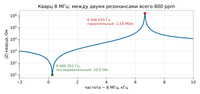
A crystal has two resonances. At the series one the impedance is minimal and equal to the losses, at the parallel one it is maximal:
| Frequency | Value in the model | Impedance |
|---|---|---|
| series resonance | 8000261 Hz | 10.0 Ω |
| parallel resonance | 8006659 Hz | 1.58 MΩ |
Between them there are only 6398 Hz — 800 parts per million. In this narrow band the crystal behaves like an inductance, and only here can a Pierce circuit oscillate: the two capacitors to ground and the crystal form a resonant circuit that needs exactly an inductance. Where inside this band the frequency lands is decided by the load capacitance.
174.3 Load capacitance and frequency shift
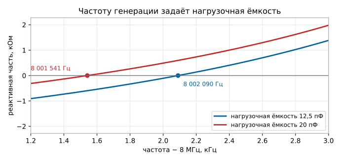
Crystals are made "for a load capacitance": 12.5 pF, 20 pF, 8 pF. This is not a property of the crystal itself but the condition under which the frequency equals the nominal one. The model of the crystal with different capacitances:
| Load capacitance | Oscillation frequency | Shift from series resonance |
|---|---|---|
| 12.5 pF | 8002090 Hz | +229 ppm |
| 20 pF | 8001541 Hz | +160 ppm |
The difference between them is 548 Hz, or 68.6 ppm. So a 12.5 pF crystal used with capacitors for 20 pF gives 68.6 ppm of error — while the tolerance of the crystal itself is usually ±10…30 ppm.
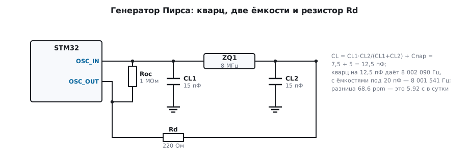
The calculation: CL = CL1 · CL2 / (CL1 + CL2) + Cstray, where CL1 and CL2 are the two
capacitors to ground (not to be confused with the motional capacitance C1 from 174.1), and
Cstray is the capacitance of the traces and pins, usually 3…5 pF. For a 12.5 pF crystal and
Cstray of 5 pF you need 7.5 pF from the capacitor pair, that is CL1 = CL2 = 15 pF.
174.4 Clocks: from ppm to seconds
As a system clock, 68.6 ppm is a trifle: UART at 115200 baud survives even 2 %. For timekeeping it is a lot. The conversion is simple: 1 ppm is 0.0864 seconds per day.
| Drift | Per day | Per month |
|---|---|---|
| 10 ppm | 0.86 s | 26 s |
| 68.6 ppm | 5.92 s | 3.0 min |
| 100 ppm | 8.64 s | 4.3 min |
The 32768 Hz watch crystal is a separate story: its frequency depends on temperature parabolically, with a coefficient of about −0.035 ppm/°C² and the turnover point at 25 °C. At 0 °C that is −21.9 ppm, so the clock loses 1.89 s per day, and no capacitance trimming will remove this — only temperature compensation in software or a ready-made compensated RTC module.
174.5 Start-up: gain margin
The oscillator starts if the amplifier supplies more than the crystal loses: the "negative resistance" of the circuit must be several times larger than the ESR of the resonator.
You can estimate the margin before layout: compute the critical transconductance of the crystal
gm_crit = 4 · ESR · (2πf)² · (C0 + CL)² and compare it with the documentation of the
microcontroller. It gives one of two things. Either the transconductance of the oscillator itself,
gm — then the ratio gm / gm_crit must be at least 5. Or the
maximum crystal transconductance Gmcritmax — on the LSE of newer families it differs for
each drive level LSEDRV — and then the crystal's gm_crit must not
exceed it. For the 8 MHz crystal from the model gm_crit is 31 µA/V. A watch crystal
with ESR 70 kΩ, C0 1.5 pF and CL 12.5 pF gives 2.33 µA/V, the same crystal with CL
6 pF gives 0.67 µA/V, 3.5 times less. The LSE oscillator is deliberately weak for the sake of
a microamp current, so it is paired with crystals of low load
capacitance.
The practical check done on the board:
- Solder a resistor of 4…5 times the maximum ESR from the crystal's documentation in series with the crystal, not the typical value: every crystal of the batch needs the margin, and only the limit is guaranteed. For the model with ESR 10 Ω that is 40…50 Ω, for a crystal with a limit of 80 Ω it is already 320…400 Ω.
- Power the board up several times, including cold and hot.
- If the oscillator still starts, there is margin; if not, you need
smaller capacitors CL1 and CL2, a crystal with lower ESR, and for a watch crystal
a stronger LSE drive mode (
LSEDRVon F0, F3, L4, G0, G4, H7,LSEMODon F411). The HSE oscillator of these series has no such setting.
The second parameter is the drive level: the power dissipated in the crystal. Too much ages the crystal and shifts the frequency, which is why the circuit has a resistor Rd in series with the output (usually hundreds of ohms): it limits the current through the crystal and also helps the symmetry of the signal.
A 32768 Hz watch crystal has an ESR of tens of kilohms, and for it gain margin is the main problem: its current is in microamps, and any leakage across the board (flux, moisture) shunts the circuit and stops the oscillation.
174.6 Pitfalls
The frequency is off by tens of ppm, the crystal is "bad". The capacitors do not match the load capacitance: 12.5 versus 20 pF is 68.6 ppm.
The stray capacitance of the traces was forgotten. Cstray of 3…5 pF is part of the load capacitance: without it the capacitors come out larger than needed.
The oscillator does not start on some boards. There is no gain margin; check with a resistor of 4…5 maximum ESR, not "on one board at room temperature".
The clock loses a few seconds a day and runs differently in summer. The parabola of the watch crystal: −0.035 ppm/°C², at 0 °C — 1.89 s per day.
The watch crystal stopped starting after the board was washed. Surface leakage shunts a resonator with an ESR of tens of kilohms — clean and dry the board.
CL1 and CL2 made too large "for reliability". They increase the current through the crystal and reduce the gain margin — the opposite of the intended effect.
174.7 Summary
- The 8 MHz crystal in the model: L1 49.47 mH, C1 8 fF, R1 10 Ω, C0 5 pF, Q factor 249000.
- Two frequencies: series resonance 8000261 Hz at 10.0 Ω and parallel 8006659 Hz at 1.58 MΩ — 800 ppm between them.
- A load capacitance of 12.5 pF gives 8002090 Hz, 20 pF gives 8001541 Hz; choosing the wrong one costs 68.6 ppm, which is 5.92 s per day.
CL = CL1 · CL2 / (CL1 + CL2) + Cstray: for 12.5 pF and Cstray of 5 pF, CL1 = CL2 = 15 pF.- Gain margin is estimated before layout from
gm_critand checked on the board with a resistor of 4…5 maximum ESR (for the model, 40…50 Ω) in series with the crystal.
Next: section 175 "Comparators: delay, open-drain output, hysteresis, window comparator".