 Embedded HandbookApps
207. The assembly workbench: static, SMD soldering, cleaning
Series production is assembled by the factory (section 199), but the first boards, repairs and rework
are soldered by hand — on the same desk where the multimeter, the oscilloscope
and the bench power supply live (section 36а). This section is about the desk itself: why
a microcontroller is killed by a discharge your hand does not even feel, how
the workbench grounding is arranged and how to check it with a multimeter in
a minute, at what temperatures solder melts and why a hot-air gun is dangerous, how
to solder an LQFP-48 and tiny 0603 parts without bridges or "tombstones", and why
"no-clean" flux does not mean "harmless". The numbers come from the datasheets of
STM32F103 and STM32F407 in the packs (run _verify/solder207/ds207.py)
and from the calculations in calc207.py in the same folder.
Terms used in the documentation
Term Meaning ESD protected area (EPA) a static-safe zone: a bench where everything has a path to ground charged device model (CDM) the chip itself is charged and discharges wrist strap an antistatic band worn on the wrist dissipative mat a mat that conducts, but through megohms air ionizer removes charge from insulators no-clean flux flux whose residues are designed to be harmless solder wick, desoldering braid a copper braid that soaks up excess solder drag soldering the tip is dragged along a row of pins surface insulation resistance (SIR) the insulation resistance of the board surface eutectic alloy an alloy that melts at a single point, not over a range
207.1 Static: why a chip dies silently and not right away
A human is a charged capacitor of about 150 pF. How many volts it carries depends on the floor, the shoes and the weather: by typical estimates from ESD practice, a walk across a synthetic carpet in dry air charges you to 15–35 kV, the same walk at 65–90 % humidity to roughly 1.5 kV. This is an order of magnitude, not an exact figure: humidity decides everything. More important is something else: the threshold at which a discharge is felt at all, as a click, is about 3 kV. Everything below that happens without you noticing.
Now the chip's side. The datasheets of both F103 and F407 have an "ESD
absolute maximum ratings" table, and its numbers are the same (run ds207.py):
| Discharge model | What it simulates | F103 and F407 |
|---|---|---|
| human body (HBM) | a finger or a tool in the hand | class 2: 2000 V |
| charged device (CDM) | the chip itself is charged and discharges through a pin | class II: 500 V |
The human body model is a 100 pF capacitor discharged through
1.5 kΩ: at the rated 2 kV this gives a peak of 1.3 A with a time constant of 150 ns
and an energy of CU²/2 = 0.2 mJ (calculation calc207.py). A person charged
to 8 kV carries 4.8 mJ — 24 times more; at 15 kV it is 16.9 mJ, 84
times more. The gap between "I won't feel it" (3 kV) and "the rating is exceeded" (2 kV)
is the main reason the bench is equipped before the first soldering job:
a dangerous discharge comes with nothing you can feel.
The second row of the table is more insidious. The charged device model is when the chip itself is charged: the package picks up charge sliding along a plastic tube or tape, and then touches something grounded with a pin — the tweezers, the tip, the board. The edge of such a discharge is shorter than a nanosecond, and the rated limit is two to four times lower: 500 V. That is exactly why not only the person is grounded, but everything the chip touches.
The chip dies silently and not always right away. The discharge punctures the gate oxide — a film a few nanometres thick: with a typical dielectric strength of the order of 1 V/nm, an oxide of 5 nm needs only 5 V reaching the gate — the built-in pin protection absorbs, and must absorb, everything else (how it works and why it is not enough: section 62). If the breakdown is partial, the pin keeps working — with increased leakage — and the board passes every check, but fails weeks later at the customer's. Latent damage is visible neither to the eye nor to a tester — that is why static is fought with procedure, not with repair.
⚠️ This is about storage and assembly, not about the product in operation. A discharge into a finished device through the enclosure and connectors is a system-level problem, solved by pin protection (section 62) and the product's defences (section 203). The rated 2 kV HBM applies to a bare chip on the bench — before it is soldered in behind a TVS and an enclosure.
207.2 Wrist strap, mat, grounding
All bench protection comes down to one rule: every charge must have a path to ground — a slow one. Slow, because what matters is not the ground itself but the current with which the charge drains through it: an 8 kV discharge directly into metal means tens of amperes within nanoseconds (the 330 Ω model is in section 203.3), while through a 1 MΩ resistor the same charge drains at no more than 8 mA with a time constant of about 150 µs — no spark and no current surge.
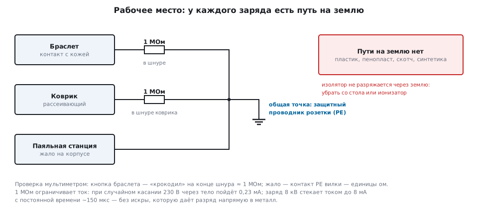
How it works:
- Wrist strap: a conductive band on the wrist, with a 1 MΩ resistor hidden in its cord. It also protects in the other direction: if the hand wearing the strap touches a 230 V live wire, 0.23 mA will flow through the body — orders of magnitude below a dangerous level. The strap works only in contact with the skin: worn over a sleeve, it is jewellery.
- Mat on the desk: not metal and not plastic, but a dissipative material: a typical surface resistance from a few megohms to a gigohm. The board and the chips lie on it, and the charge drains through the mat cord with the same 1 MΩ.
- Soldering iron: the tip is grounded directly through the station: a few ohms to the protective earth conductor of the socket. A floating tip at some potential means a discharge into the first pin it touches.
- Everything meets at one point: the protective earth conductor of the socket (PE).
🔧 A one-minute check with a multimeter. With the ohmmeter (section 36а.1): wrist strap stud to the alligator clip at the end of the cord: about 1 MΩ; much less means the resistor is punctured, "out of range" means the cord is broken. Tip to the PE contact of the station plug: a few ohms. Mat from point to point: megohms and more — here many multimeters have a measurement limit below the mat resistance, and "out of range" is not a defect in itself; what matters is that the mat does not beep like metal and is not silent like a plastic tablecloth.
What is dangerous on the desk: everything a charge cannot drain from. Plastic enclosures and boxes, foam, adhesive tape, polyethylene bags, synthetic clothing and chair upholstery hold charge for hours — they are removed from the desk, and boards are stored in dissipative or shielding bags. An insulator cannot be discharged by grounding at all: if plastic in the work zone is unavoidable, only an air ionizer removes the charge from it. And the cheapest ally is humidity: in winter, next to a radiator, the air dries out to 10–20 %, and the same actions give an order of magnitude more kilovolts than in summer.
207.3 Soldering iron and hot air: temperatures
The starting point for any temperature on the bench is the melting point of the solder.
The classic tin-lead alloy of 63 % tin and 37 % lead is
a eutectic: it melts and solidifies at a single point, 183 °C, lower than
either of the pure metals (tin 232 °C, lead 327 °C) — the composition
is chosen exactly at the minimum of the alloy. A typical lead-free alloy is
96.5 % tin, 3 % silver and 0.5 % copper (marked SAC305 —
after the composition: S, A, C and the fractions) — it melts at 217–219 °C, 34 °C above
the eutectic; the compositions and differences are checked in calc207.py.
The tip is heated not "to melting" but with a margin for heat sinking into the copper pours and the leads: the practical rule is 100–130 °C above the melting point. For tin-lead that is about 300 °C, for lead-free 330–350 °C. Higher is not faster: the flux burns off before it can clean the pad, the solder stops wetting, the tip gets covered with oxide. If the joint "won't take", nine times out of ten what is missing is not temperature but flux or contact area under pressure.
⚠️ Tip temperature is not soldering temperature. The station display shows the sensor inside the tip, not the pad. A massive ground pour draws heat away faster than a thin tip delivers it: a joint on it at an honest 300 °C on the display will stay cold. The cure is not turning the knob to maximum but a thicker tip and thermal reliefs in the layout (cross-shaped traces connecting the pad).
The hot-air gun is the second tool: it heats the whole package at once, and for desoldering
multi-pin packages or soldering a component with an exposed pad it has no
alternative on the bench. But a stream of hot air has two side
effects. The first: it blows small parts away: a 0603 chip component weighs about
2.2 mg, and an 0201 weighs 0.16 mg (volume times the density of the ceramic, calc207.py);
a narrow nozzle and minimum airflow are not a recommendation but a condition
for the neighbours' survival. The second: hot air heats everything around the target: nearby
plastic connectors melt, the glass-epoxy laminate darkens and delaminates under prolonged overheating
(the typical glass transition temperature of basic
FR-4 is about 135 °C, above it the resin is soft), and nearby chips
go through a full heating cycle with all the consequences for the moisture
in the package (207.7).
207.4 Hand soldering LQFP-48 and 0603
Assembly defects and how to see them are in the table in 200.1; here is where they come from and how to solder so they do not appear.
An 0603 chip component. Tin one pad with a thin layer, pick up the component with tweezers, bring it in and heat the tinned pad together with the end of the component — the part is seated; then solder the second terminal, and go back to the first with a drop of solder. A "tombstone" — a component standing on its end — is physics, not sloppiness: while the solder melts on one side only, the surface tension of the melt pulls that end down and lifts the opposite one. By hand the cure is simple: melt both ends not simultaneously but one after the other and completely: tack, a full joint on the second terminal, back to the first. With hot air, heat the component in the centre, not from one end.
LQFP-48 with 0.5 mm pitch (the package on the board from section 131) is soldered by hand faster than it seems — if you do not try to solder it one pin at a time:
- Tin one corner pad. Place the package according to the key (the dot is pin 1; polarity is checked before soldering, 200.1), heat the corner — the package is tacked.
- Check the alignment on all four sides: at 0.5 mm pitch a miss by half a pad is visible on the outermost pins. While one corner holds, the package can be moved by heating the tack. Then tack the diagonal corner.
- Apply gel flux to the pins along the whole side. Load a little solder onto a bevel tip and solder the side by dragging — one slow movement along the row, lightly touching the tips of the pins. The solder distributes itself over the pins while there is little of it and plenty of flux.
- Bridges between adjacent pins are not removed "one at a time": you place the braid with flux on the bridge and heat it — the braid soaks up the excess solder, and the bridge disappears completely.
🔧 Flux is a consumable, not an emergency reserve. Dragging works on fresh gel: one side, one strip of flux. Dry pins give bridges on every third pin, and you will use more braid than you would have used flux. After soldering, the gel residues on megohm circuits will have to be cleaned off — what happens if you do not is calculated in the next subsection.
207.5 Cleaning: what flux residues do to megohm circuits
Fluxes fall into two camps. Water-washable / cleanable fluxes are active: they solder well, but their residues conduct and corrode, so cleaning is mandatory. No-clean fluxes: the residues are designed to be harmless: low activity, non-corrosive, and for typical digital circuits you really can leave them alone (in 200.1 residues around joints are called normal). The catch is in the word "typical": "harmless" is about corrosion, not about resistance. The film of residues on the board is an extra resistor between adjacent nets, and its value is measured by exactly that surface insulation resistance: a clean dry board gives gigohms, a flux film that has absorbed moisture from the air gives tens or even single megohms.
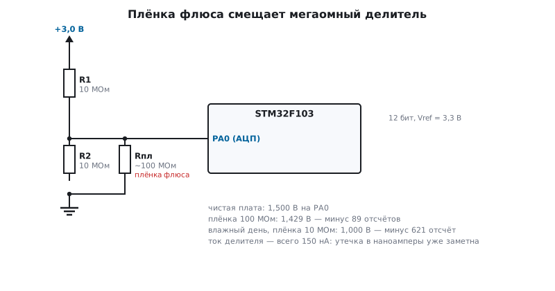
While the circuits around are in the kilohm range, megohms of leakage are invisible. Now let us calculate
a megohm one (calculation calc207.py): a battery voltage of 3.0 V is measured with a
10 MΩ + 10 MΩ divider — the divider current is only 150 nA, which is why it
was made that way. A clean board gives exactly 1.500 V at the ADC input. A flux film
of 100 MΩ — an optimistic estimate for an uncleaned area —
in parallel with the lower leg turns it into 9.09 MΩ: the input is 1.429 V,
an offset of −71 mV, and a 12-bit ADC with Vref = 3.3 V is off by 89 counts.
On a humid day the same film drops to 10 MΩ — the input is 1.000 V,
minus 621 counts: a third of the measured value is gone, although the circuit
is fine, the firmware is honest and yesterday everything added up.
Hence the rule: clean everything high-impedance and precise. Megohm dividers and ADC inputs, guard rings (section 181), crystal pins — a flux film shunts the resonator and stops oscillation (section 174), op-amp circuitry with large resistors. The procedure: isopropyl alcohol or a dedicated flux remover, a stiff brush, wiping with a lint-free wipe — and mandatory drying: freshly dissolved flux, spread with a brush and left to dry as a puddle, is worse than untouched flux, because as a thin film it now covers the whole board, not just the area around the joint. Cleaning means washing off and removing what has dissolved, not spreading it over the surface.
⚠️ Do not mix the camps. You soldered with no-clean flux, then "just in case" wiped one corner with alcohol — and got exactly that smeared layer. Either the board lives with untouched no-clean residues, or it is cleaned completely and dried.
207.6 Microscope, magnifier and tweezers
For hand-soldered SMD, optics matter more than a helping hand, and the list is shorter than it seems:
| Tool | What it gives | When it is enough |
|---|---|---|
| ×10 magnifier | inspection of joints, bridges, polarity (200.1) | all inspection of 0603–0805 and LQFP |
| ×7–×45 stereo microscope | depth and working distance for the iron | soldering 0402 and smaller, 0.4 mm pitch, finding microcracks |
| USB microscope | photos of defects on screen and in a report | documenting; the image lag gets in the way of soldering under it |
Soldering "by eye" and checking with a magnifier is the normal mode for 0603 and LQFP-48; a microscope becomes mandatory where the eye is no longer enough — at 0.4 mm pitch and with 0402/0201 packages. A stereo microscope needs only low magnification: at ×10 you can see the wetting of the fillet, and a working distance of about ten centimetres leaves room for your hands and the tip.
Tweezers: straight and bent, with fine tips, stainless and non-magnetic — magnetised ones pick up neighbouring small parts in clusters. Hold a component by the sides of its body, not by the terminals: on chip components the terminals are the metallisation on the ends of the ceramic, and metallisation chipped by the tweezer tips turns into an open joint that solder cannot fix. For chips taken from tubes and tapes, metal tweezers are also a grounded (through the hand in the wrist strap) CDM discharge path: the rated 500 V limit builds up on a package easily, so pulling a chip out of the tape with bare tweezers and no wrist strap is the worst combination on the bench.
207.7 Moisture and MSL: baking packages before soldering
A plastic chip package is hygroscopic: it absorbs moisture from the air, and its sensitivity level is specified by the manufacturer as the MSL (the term is in the terms box of 199; the same place has the rule to send chips to the factory in unopened dry packaging). On your own bench the rule is exactly the same, only there is nobody but you to watch it.
The failure physics is "popcorning": during soldering the absorbed water boils inside
the package, and the saturated vapour pressure rises steeply with temperature —
at the 217 °C of lead-free soldering it is already about 2.2 MPa, more than twenty
atmospheres, at the 250 °C of a hot-air gun close to 4 MPa (calc207.py). The vapour bursts
the package from inside: delamination, a crack, broken bond wires of
the die — sometimes with an audible click, more often silently, with the same latent
fate as with static.
Bench practice:
- an opened bag of chips has a limited floor life — hours or days depending on the MSL and the humidity; the specific time is printed on the dry-pack label;
- a package past its floor life is baked before soldering: the typical profile from the same label is about a day at 125 °C, for heat-resistant packaging;
- loose parts are better stored in a jar with silica gel or in a dry cabinet than in a desk drawer;
- hand soldering with an iron heats the lead, not the package — the risk of "popcorning" is minimal; hot air and any reflow soldering heat the whole package — for them MSL applies in full.
207.8 Pitfalls
The board passed all checks and died at the customer's a month later. Static: a partially punctured oxide works until it breaks completely. Inspection and a tester do not see latent damage — only the procedure helps: wrist strap, mat, grounded tip, dissipative packaging (207.1–207.2).
The wrist strap is on — the chips still die. The strap is over the sleeve, the cord is broken, or the resistor has dried out and punctured. The ohmmeter check takes a minute: stud to alligator clip about 1 MΩ. And the wrist strap does not protect against a charged-device discharge: a chip charged by rubbing against its tube will discharge into the grounded tweezers — the limit for this model is only 500 V.
Lead-free solder "won't take" with the usual settings. The melting point is 34 °C above the eutectic: 217–219 °C against 183 °C. Tip at 330–350 °C, more flux, a thicker tip — not "hold it longer": long heating already eats the flux and heats the package.
The joint on a massive pour is cold at an honest 300 °C on the display. The display measures the tip, not the pad: the pour carries heat away faster than a thin tip delivers it. A thicker tip, thermal reliefs in the layout — not the temperature knob at maximum.
After hot air, small parts are missing around the repair site. The airflow blew them away: 0603 weighs 2.2 mg, 0201 weighs 0.16 mg. Narrow nozzle, minimum airflow, cover the neighbours; after any hot-air work, inspect the area as in 200.1.
The ADC "drifted" after a repair, the circuit is fine. A flux film in a megohm circuit: 100 MΩ in parallel with a 10 MΩ divider leg is minus 89 counts, on a humid day hundreds (207.5). Clean completely and dry; a half-hearted wipe with alcohol smears the residues and makes it worse.
A chip clicked during hot-air soldering. "Popcorning": moisture in the package from a bag opened a month ago, vapour at 2–4 MPa. Packages past their MSL floor life are baked for about a day at 125 °C before soldering (207.7).
207.9 Summary
- The rated ESD robustness of the pins of F103 and F407 is the same: 2000 V for the human body model (class 2) and 500 V for the charged device model (class II) — from the ESD tables in the datasheets.
- The danger zone is invisible: a discharge is felt from about 3 kV, while the rating ends at 2 kV; a person at 8 kV carries 4.8 mJ — 24 times more energy than the rated HBM model (100 pF through 1.5 kΩ: 1.3 A, 0.2 mJ).
- Bench grounding: everything to one point through 1 MΩ: the wrist strap and the mat drain in milliamps (8 kV → no more than 8 mA, ~150 µs), and on touching 230 V the same resistor limits the current to 0.23 mA; the tip goes directly, a few ohms. Check each path with an ohmmeter.
- Solder: the 63/37 eutectic melts at 183 °C (below both pure metals), lead-free 96.5/3/0.5 at 217–219 °C; the tip is 100–130 °C above the melting point: ~300 °C and 330–350 °C. Hot air blows away 0603 (2.2 mg) and heats the neighbours — narrow nozzle and minimum airflow.
- LQFP-48 is soldered by tacking two corners and dragging with gel flux, bridges are removed with braid; "tombstones" of small parts come from melting one end.
- Flux residues are a resistor: a 100 MΩ film in a 10 + 10 MΩ divider shifts a 12-bit ADC by 89 counts, a humid one (10 MΩ) by 621; megohm circuits, crystals and guard rings are cleaned completely and dried.
- Moisture in the package during soldering means vapour at 2.2 MPa at 217 °C and ~4 MPa at 250 °C: packages opened beyond their MSL floor life are baked (typically a day at 125 °C), especially before hot air.
Next: section 208 "A device powered from 230 V mains: safety and power supply".