 Embedded HandbookApps
15д. The precision ADS1256 ADC over SPI: 24 bits, 8 inputs, PGA up to 64, buffer, rates up to 30 000 samples per second, self-calibration and synchronization
In 15г the ADS1220 measured a bridge and a PT100: four inputs, up to 2000 samples per second, the reference taken from the sensor. The ADS1256 is for a different job: many inputs and high speed. Eight inputs (or four pairs), gain up to 64, an input buffer, rates from 2.5 to 30 000 samples per second, its own 7.68 MHz crystal and offset and gain calibration on command. Here: the driver — the commands and eleven registers, the t6 pause between a command and the read, SPI mode 1 and the clock limit, a module board with a 5 V supply and 3.3 V logic, the buffer and the input limits, speed and noise, continuous reading with RDATAC, cycling through eight inputs with SYNC and WAKEUP — how many results to discard after an input change and what rate is left per channel, calibration after a gain or rate change, and the pitfalls. What delta-sigma, an averaging filter, a PGA and 24 bits in two's complement are — see 15г; how the built-in ADC catches up with the neighbouring channel — see 180.3, here the cause is different.
Sources: RM0008 (DocID13902 Rev 17): SPI pins — table 25, p. 166; SPI1
without remap — PA4–PA7, p. 185; AFIO_EXTICR1, p. 190; EXTI_FTSR,
p. 211; BR[2:0] = 100 — fPCLK/32, 101 — fPCLK/64, p. 743; CPOL and
CPHA, p. 744; BSY, p. 745. DocID13587 Rev 17 (STM32F103x8/xB):
PA4–PA7 are the SPI1 pins, PA4–PA7 and PB0 are not 5 V tolerant, p. 29.
The project has no document on the ADS1256, and there is no open driver
on disk either: Klipper and the other open projects
do not have one. The command codes, register addresses and fields, reset
values, DRATE codes, the 7.68 MHz clock, the t6 and t11 pauses, the SPI
clock limit, the input limits with and without the buffer and the input
impedance come from the manufacturer's documentation and were not
checked; they are built into the model and checked against it. All
numbers below come from a run of the driver _verify/adc15f/ads15f.c,
built by arm-none-eabi-gcc 12.2.1 for the Cortex-M3 and run in QEMU 7.2
(netduino2) against our own model of the ADS1256 in Python 3.11; the
firmware is built by armclang 6.24 for the Cortex-M3. The numbers
describe the model, not the chip.
What it is called in the documentation
Original Meaning analog input common (AINCOM) the common input: the minus side of single-ended measurements input buffer enable (BUFEN) turning on the input buffer: the input barely loads the source absolute input voltage input voltage relative to AGND master clock input (CLKIN), τCLKIN the clock input; the period of that clock DIN-to-DOUT delay (t6) the pause from a read command to the first bit of the answer read data continuous (RDATAC), stop read data continuous (SDATAC) every result shifted out without a command; stopping that SYNC / WAKEUP commands stop the filter; start it again multiplexer cycling going round the inputs self offset / self gain calibration (SELFOCAL, SELFGCAL) self-calibration of zero / of gain system offset / system gain calibration (SYSOCAL, SYSGCAL) calibration by the signal at the input offset / full-scale calibration registers (OFC, FSC) zero and scale correction registers auto-calibration (ACAL) calibration by itself after a settings change noise-free resolution resolution without noise: the noise swing is below one code
15д.1 How it differs from the ADS1220
| ADS1220 (15г) | ADS1256 | |
|---|---|---|
| inputs | 4, pairs and against AVSS | 8 single-ended against AINCOM or 4 pairs, any with any |
| gain | 1…128 | 1…64 |
| input buffer | none | yes, BUFEN |
| data rate | 20…1000 SPS, turbo 40…2000 | 2.5…30 000 SPS, 16 DRATE codes |
| clock | its own internal one | a 7.68 MHz crystal or oscillator on CLKIN |
| reference | its own 2.048 V, REF0, REF1, supply | external only, VREFP − VREFN |
| calibration | none (offset — inputs shorted) | SELFCAL, SYSOCAL, SYSGCAL commands and OFC, FSC registers |
| supply | 3.3 V | AVDD 5 V, DVDD 1.8…3.6 V |
The range is ±2·VREF / PGA: with a 2.5 V reference and a gain of 1 that is ±5 V, one code is 596.047 nV. The code is 24 bits in two's complement, as in 15г.4; +2·VREF / PGA gives 0x7FFFFF.
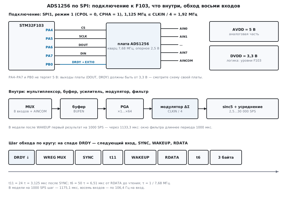
15д.2 Connecting it to the F103, the board and the buffer
| ADS1256 pin | STM32F103 | Purpose |
|---|---|---|
| SCLK | PA5 | SPI1 clock |
| DIN | PA7 | MOSI: commands and data into the chip |
| DOUT | PA6 | MISO: the answer |
| CS | PA4 | chip select, a plain output |
| DRDY | PB0 | "ready", EXTI0 on the falling edge |
| AVDD, DVDD, AGND, DGND | 5 V, 3.3 V, ground | common ground with the microcontroller |
The pins are as in 15г.2: SPI1 without remap on PA4–PA7 (RM0008,
p. 185), SCK and MOSI — alternate function push-pull, MISO — input
(table 25, p. 166), DRDY — EXTI0 on the falling edge (AFIO_EXTICR1,
p. 190, EXTI_FTSR, p. 211). SPI mode 1 (18.2): the chip puts a bit out
on the rising clock edge and it must be read on the falling one
(manufacturer's documentation).
static void spi1_init(void)
{
    RCC->APB2ENR |= RCC_APB2ENR_IOPAEN | RCC_APB2ENR_IOPBEN | RCC_APB2ENR_AFIOEN | RCC_APB2ENR_SPI1EN;
    GPIOA->BSRR = 1u << 4;                              /* CS вверх до настройки вывода */
    /* PA4 — выход 50 МГц (0011), PA5 и PA7 — альтернативная функция push-pull (1011), PA6 — вход (0100) */
    GPIOA->CRL = (GPIOA->CRL & 0x0000FFFFu) | 0xB4B30000u;
    GPIOB->CRL = (GPIOB->CRL & ~0xFu) | 0x8u;           /* PB0 — вход с подтяжкой (1000) */
    GPIOB->BSRR = 1u << 0;
    SPI1->CR1 = SPI_CR1_MSTR | SPI_CR1_CPHA | SPI_CR1_BR_2 | SPI_CR1_BR_0 | SPI_CR1_SSM | SPI_CR1_SSI;  /* режим 1, /64 */
    SPI1->CR1 |= SPI_CR1_SPE;
}
SPI clock. The SCLK period must be at least 4 τCLKIN (manufacturer's
documentation): τ = 1 / 7.68 MHz = 130.208 ns, the limit is 520.8 ns,
that is 1.92 MHz. SPI1 on the F103 runs at 72 MHz: BR = 100 gives
72 / 32 = 2.25 MHz — already too fast, BR = 101 — 1.125 MHz (p. 743).
A byte at 1.125 MHz takes 7.111 µs.
Supply. The analog part needs AVDD = 5 V, the digital part DVDD from 1.8 to 3.6 V (manufacturer's documentation). DOUT and DRDY output the DVDD level, and PA4–PA7 and PB0 of the F103 are not 5 V tolerant (DocID13587, p. 29): DVDD must be 3.3 V. Common module boards take 5 V and make the 3.3 V for DVDD with their own regulator, and carry the 7.68 MHz crystal and a 2.5 V reference — but boards differ: check the schematic of yours, we did not check any board. If DVDD on the board is 5 V, it cannot be wired to the F103 directly.
Buffer. Without the buffer the input is switched capacitors and the source charges them: the input impedance is about 150 kΩ / PGA, with the buffer 80 MΩ (manufacturer's documentation). But with the buffer the input must stay from AGND to AVDD − 2 V, without it from AGND − 0.1 V to AVDD + 0.1 V. In the model, AVDD = 5 V, AIN0 against AINCOM, ×1:
| AIN0 | With buffer | Without buffer |
|---|---|---|
| 1 V | 1 000 000 µV | 1 000 000 µV |
| 2.9 V | 2 900 000 µV | 2 900 000 µV |
| 3.3 V | 3 000 000 µV | 3 300 000 µV |
| 4.5 V | 3 000 000 µV | 4 500 000 µV |
Above 3 V the buffered input shows 3 V — no error, no flag. A 20 mV source with source resistance Rs:
| Rs | Buffer, ×1 | Buffer, ×64 | No buffer, ×1 | No buffer, ×64 |
|---|---|---|---|---|
| 0 | 20 000 µV | 20 000 µV | 20 000 µV | 20 000 µV |
| 1 kΩ | 20 000 µV | 20 000 µV | 19 867 µV | 14 019 µV |
| 10 kΩ | 19 997 µV | 19 998 µV | 18 750 µV | 3797 µV |
A 10 kΩ divider without the buffer loses 6.25 % at ×1 and 81 % at ×64. The rule: a source with any resistance — the buffer; a signal above 3 V — a divider and the buffer, or no buffer but a low-impedance source (180.2).
15д.3 Commands, registers and the t6 pause
| Byte | Command | What it does |
|---|---|---|
| 0x00, 0xFF | WAKEUP | start after SYNC or STANDBY |
| 0x01 | RDATA | after the t6 pause — three bytes of the result |
| 0x03 | RDATAC | from now on every result on the DRDY falling edge, no command |
| 0x0F | SDATAC | stop that; listen to commands again |
| 0x1r, 0n | RREG | read n + 1 registers from address r; after the t6 pause |
| 0x5r, 0n | WREG | write n + 1 registers from address r |
| 0xF0 | SELFCAL | self-calibration of zero and gain |
| 0xF1, 0xF2 | SELFOCAL, SELFGCAL | zero only; gain only |
| 0xF3, 0xF4 | SYSOCAL, SYSGCAL | zero and scale by what is at the input now |
| 0xFC | SYNC | stop the filter until WAKEUP |
| 0xFD | STANDBY | sleep until WAKEUP |
| 0xFE | RESET | registers to their defaults |
| Address | Register | Fields | After RESET |
|---|---|---|---|
| 0 | STATUS | 7:4 — ID (3 for the ADS1256), 3 — ORDER, 2 — ACAL, 1 — BUFEN, 0 — DRDY |
0x3x |
| 1 | MUX | 7:4 — PSEL, 3:0 — NSEL: 0…7 — AIN0…AIN7, 1xxx — AINCOM |
0x01 |
| 2 | ADCON | 6:5 — CLK (clock on D0/CLKOUT), 4:3 — SDCS (open-circuit currents), 2:0 — PGA: 1, 2, 4 … 64 |
0x20 |
| 3 | DRATE | rate code (15д.4) | 0xF0 |
| 4 | IO | 7:4 — directions of D3…D0, 3:0 — their levels | 0xE0 |
| 5–7 | OFC0…OFC2 | zero correction, signed 24 bits, low byte first | — |
| 8–10 | FSC0…FSC2 | scale correction, 24 bits, low byte first | — |
All of this comes from the manufacturer's documentation; the model and
the driver agree with it, but no chip was connected. ADCON = 0x20 after
reset puts the 7.68 MHz clock out on D0/CLKOUT; if it is not needed, the
driver writes CLK = 00 — an extra signal next to the inputs is of no
use.
t6. After RDATA and RREG the chip needs 50 τCLKIN to prepare the
answer: 50 × 130.208 ns = 6.51 µs. The F103 SPI sends bytes back to back,
and the next clock would come half a period later — so the driver splits
the frame into two transfers and waits ADS_T6_US = 7 µs between them:
/* RREG: два байта команды, пауза t6 — и только потом ответ, всё в одном кадре */
void ads_rreg(ads_t *d, uint32_t reg, uint8_t *v, uint32_t n)
{
    uint8_t tx[11] = {(uint8_t)(ADS_CMD_RREG | (reg & 15u)), (uint8_t)((n - 1u) & 15u)}, rx[11];
    ads_port_cs(0);
    ads_port_xfer(tx, rx, 2);
    ads_port_delay_us(ADS_T6_US);
    ads_port_xfer(tx + 2, v, n);                        /* на DIN — нули */
    ads_port_cs(1);
    d->frames++;
    d->bytes += n + 2u;
}
After SYNC and RDATAC, before the next command — t11 = 24 τ = 3.125 µs
(ADS_T11_US = 4 µs, ads_cmd waits for it); after the other commands —
4 τ = 0.52 µs, and raising and lowering CS takes that long anyway.
/* SDATAC на случай, если микросхема осталась в RDATAC, RESET, первый результат — и пять регистров */
int ads_reset(ads_t *d, uint8_t r[5])
{
    ads_cmd(d, ADS_CMD_SDATAC);
    (void)ads_port_wait_drdy(0);
    ads_cmd(d, ADS_CMD_RESET);
    if (!ads_port_wait_drdy(ADS_TIMEOUT_US))
        return ADS_E_TIMEOUT;
    ads_rreg(d, ADS_STATUS, r, 5);
    for (uint32_t i = 0; i < 5u; i++)
        d->reg[i] = r[i];
    return r[0] >> ADS_ID_POS == ADS_ID ? ADS_OK : ADS_E_ID;
}
In the model the reset — SDATAC, RESET, the first result at 30 000 SPS
after 166.7 µs and RREG of five registers — took 237.7 µs and read
30 01 20 F0 E0: ID = 3, MUX, ADCON, DRATE and IO as in the table. Setup
with ads_config — the WREG frame 50 03 02 08 00 A1 (buffer, AIN0 against AINCOM,
CLKOUT off, ×1, 1000 SPS) and the read back — 92.3 µs; it read
32 08 00 A1 E0: in STATUS DRDY = 0, and the driver compares only ORDER,
ACAL and BUFEN. Frames at 1.125 MHz: a command — 7.1 µs, RREG of
one register — 28.3 µs, RDATA — 35.4 µs, three bytes without a
command — 21.3 µs, WREG of four registers — 42.7 µs.
15д.4 Code, data rate and noise
Code to volts. Input = code × 2·VREF / (PGA × (2²³ − 1)):
/* код → микровольты: вход = код × 2·VREF / (PGA × (2^23 − 1)); PGA 110 и 111 — оба ×64 */
int32_t ads_uv(int32_t code, uint32_t vref_uv, uint32_t pga)
{
    uint32_t sh = pga > ADS_PGA64 ? ADS_PGA64 : pga;
    int64_t x = (int64_t)code * 2 * vref_uv;
    int64_t den = (int64_t)ADS_FS << sh;
    return (int32_t)(x >= 0 ? (x + den / 2) / den : -((-x + den / 2) / den));
}
In the model, VREF = 2.5 V, the difference AIN0 − AIN1 after SELFCAL:
| PGA | Range | One code | +1 mV | +50 mV | −50 mV |
|---|---|---|---|---|---|
| 1 | ±5000 mV | 596.047 nV | 1678 | 83 886 | −83 886 |
| 8 | ±625 mV | 74.506 nV | 13 422 | 671 089 | −671 088 |
| 64 | ±78.125 mV | 9.313 nV | 107 374 | 5 368 709 | −5 368 708 |
The extreme codes are 5 000 000 and −5 000 001 µV. A single-ended input against AINCOM at ground is never negative: AIN0 = 0, 1, 3.3 and 4.9 V gave codes 0, 1 677 721, 5 536 481 and 8 220 835 — half of the scale works, 23 bits. If the sign is needed — AINCOM at 2.5 V or a pair of inputs.
Data rate. In the model the filter is a sinc5 with a 1/30 000 s step and an average of N of its results, N = 30 000 / DR (a model assumption; by the manufacturer's documentation the real filter is built the same way, but we did not check its timings). The first result after WAKEUP comes after (N + 4) / 30 000 s, then every N / 30 000 s:
DRATE code |
SPS | N | After WAKEUP | Period |
|---|---|---|---|---|
| 0xF0 | 30 000 | 1 | 166.7 µs | 33.3 µs |
| 0xE0 | 15 000 | 2 | 200 µs | 66.7 µs |
| 0xD0 | 7500 | 4 | 266.7 µs | 133.3 µs |
| 0xC0 | 3750 | 8 | 400 µs | 266.7 µs |
| 0xB0 | 2000 | 15 | 633.3 µs | 500 µs |
| 0xA1 | 1000 | 30 | 1133.3 µs | 1000 µs |
| 0x92 | 500 | 60 | 2133.3 µs | 2000 µs |
| 0x82 | 100 | 300 | 10 133.3 µs | 10 000 µs |
| 0x72 | 60 | 500 | 16 800 µs | 16 666.7 µs |
| 0x63 | 50 | 600 | 20 133.3 µs | 20 000 µs |
| 0x53 | 30 | 1000 | 33 466.7 µs | 33 333.3 µs |
| 0x43 | 25 | 1200 | 40 133.3 µs | 40 000 µs |
| 0x33 | 15 | 2000 | 66 800 µs | 66 666.7 µs |
| 0x23 | 10 | 3000 | 100 133.3 µs | 100 000 µs |
| 0x13 | 5 | 6000 | 200 133.3 µs | 200 000 µs |
| 0x03 | 2.5 | 12 000 | 400 133.3 µs | 400 000 µs |
At 30 000 SPS the first result comes after five periods, at 1000 — after 1.13 periods, at 2.5 — after almost one.
Noise. In the model the input noise is √((30 µV / PGA)² + (1.5 µV)²) × √(DR / 30 000) (a model assumption, not data from a document). 256 results each through RDATAC, the input shorted at 2.5 V; effective bits are log₂(4·VREF / PGA / noise), noise-free — by a swing of 6.6 noise:
| SPS | ×1: noise | bits | noise-free | ×64: noise | bits | noise-free |
|---|---|---|---|---|---|---|
| 30 000 | 31.214 µV | 18.3 | 15.6 | 1.528 µV | 16.6 | 13.9 |
| 7500 | 15.343 µV | 19.3 | 16.6 | 0.79 µV | 17.6 | 14.9 |
| 1000 | 5.5 µV | 20.8 | 18.1 | 0.285 µV | 19.1 | 16.3 |
| 100 | 1.668 µV | 22.5 | 19.8 | 0.094 µV | 20.7 | 17.9 |
| 10 | 0.562 µV | 24.1 | 21.4 | 0.031 µV | 22.3 | 19.5 |
| 2.5 | 0.296 µV | 25 | 22.3 | 0.015 µV | 23.3 | 20.6 |
The slower, the quieter: in the model every four-fold slowdown gives a bit. More than 24 effective bits at ×1 and 2.5 SPS is not a mistake: the noise is below one code, and 24 bits can no longer tell it apart. At 30 000 SPS a gain of ×64 lowers the input noise 20 times, but the range 64 times: the bits go down.
15д.5 DRDY, RDATA and RDATAC
The ADS1256 converts continuously: every period DRDY falls, and the result stays in the chip until the next one. There are two ways to read it.
RDATA — a command, the t6 pause, three bytes: 35.4 µs at 1.125 MHz. At 30 000 SPS the period is 33.3 µs, and RDATA cannot keep up: in the model 3000 results in a row took 106 333.3 µs and 190 results were lost — new ones overwrote them while the read was going on.
RDATAC — the command once, then three bytes on every DRDY falling edge with no command: 21.3 µs, the bus is busy 64 % of the time. In the model 3000 results took 100 010.2 µs, 1 was lost — the one that had been lying unread since before RDATAC.
/* RDATAC: дальше каждый результат выдвигается по спаду DRDY без команды; команды не слышны до SDATAC */
void ads_rdatac_start(ads_t *d)
{
    (void)ads_port_wait_drdy(0);
    ads_cmd(d, ADS_CMD_RDATAC);
}

int ads_rdatac_read(ads_t *d, int32_t *code)
{
    uint8_t z[3] = {0, 0, 0}, b[3];
    if (!ads_port_wait_drdy(ADS_TIMEOUT_US))
        return ADS_E_TIMEOUT;
    ads_frame(d, z, b, 3);
    *code = ads_s24(b);
    return range(*code);
}

int ads_rdatac_stop(ads_t *d)
{
    if (!ads_port_wait_drdy(ADS_TIMEOUT_US))
        return ADS_E_TIMEOUT;
    ads_cmd(d, ADS_CMD_SDATAC);
    return ADS_OK;
}
In RDATAC the chip hears only SDATAC and RESET (manufacturer's
documentation): RREG and WREG will not get through before SDATAC (15д.7).
After ads_rdatac_stop the registers read again — 33 08 00 F0 E0. The
model does not count processor time: on a real F103 reading in the EXTI
handler adds its own microseconds.
STANDBY. The chip sleeps until WAKEUP: in the model waiting for DRDY
after STANDBY returned ADS_E_TIMEOUT, and after WAKEUP the first result
came after 1133.3 µs — as after SYNC.
15д.6 Inputs in a cycle, SYNC and calibration
Changing the input without SYNC. The filter collects samples all the
time, and a MUX write does not stop it (a model assumption). Right after
the write a result is a mix of the old input and the new one. In the
model AIN0 = 1 V, AIN1 = 2 V, ads_set switches MUX, then results in a
row; the share of the new input:
| SPS | When MUX was written | 1st | 2nd | 3rd | 4th | 5th |
|---|---|---|---|---|---|---|
| 30 000 | at the start of a period | 0 % | 3 % | 38 % | 88.8 % | 100 % |
| 30 000 | in the middle of a period | 0.4 % | 16.6 % | 70.6 % | 98.4 % | 100 % |
| 3750 | at the start of a period | 53.7 % | 100 % | 100 % | 100 % | 100 % |
| 3750 | in the middle of a period | 17 % | 100 % | 100 % | 100 % | 100 % |
| 1000 | at the start of a period | 87.7 % | 100 % | 100 % | 100 % | 100 % |
| 1000 | in the middle of a period | 41.2 % | 100 % | 100 % | 100 % | 100 % |
| 10 | at the start of a period | 99.9 % | 100 % | 100 % | 100 % | 100 % |
| 10 | in the middle of a period | 49.9 % | 100 % | 100 % | 100 % | 100 % |
Below 30 000 SPS one result has to be discarded, at 30 000 four. It is simpler not to guess: SYNC clears the filter, WAKEUP starts it again, and the first result after WAKEUP belongs entirely to the new input.
In a cycle. This is how the manufacturer's documentation says to go round the inputs: on the DRDY falling edge — WREG MUX of the next input, SYNC, WAKEUP and only then RDATA. What is read is the result of the previous input: it stays in the chip while the filter collects the new one.
/* выбрать вход и начать заново: WREG MUX, SYNC (фильтр стоит и пуст), WAKEUP (пошёл) */
void ads_scan_start(ads_t *d, uint8_t mux)
{
    ads_wreg(d, ADS_MUX, &mux, 1);
    d->reg[ADS_MUX] = mux;
    ads_cmd(d, ADS_CMD_SYNC);
    (void)ads_port_wait_drdy(0);                        /* старый спад — не наш */
    ads_cmd(d, ADS_CMD_WAKEUP);
}

/* по кругу: спад DRDY — следующий вход, SYNC, WAKEUP, и только потом RDATA — результат прежнего входа
 * лежит в микросхеме, пока новый фильтр копит отсчёты */
int ads_scan_next(ads_t *d, uint8_t next, int32_t *code)
{
    if (!ads_port_wait_drdy(ADS_TIMEOUT_US))
        return ADS_E_TIMEOUT;
    ads_wreg(d, ADS_MUX, &next, 1);
    d->reg[ADS_MUX] = next;
    ads_cmd(d, ADS_CMD_SYNC);
    ads_cmd(d, ADS_CMD_WAKEUP);
    return ads_read_data(d, code);
}
Eight inputs AIN0…AIN7 against AINCOM, 0.2…2.3 V on them, two rounds each:
| SPS | Step | All inputs | Per input | Filter window |
|---|---|---|---|---|
| 30 000 | 208.4 µs | 4797.6 Hz | 599.7 Hz | 166.7 µs |
| 7500 | 308.4 µs | 3242.1 Hz | 405.3 Hz | 266.7 µs |
| 1000 | 1175.1 µs | 851 Hz | 106.4 Hz | 1133.3 µs |
| 100 | 10 175.1 µs | 98.3 Hz | 12.3 Hz | 10 133.3 µs |
| 50 | 20 175.1 µs | 49.6 Hz | 6.2 Hz | 20 133.3 µs |
| 10 | 100 175.1 µs | 10 Hz | 1.2 Hz | 100 133.3 µs |
The error on no input exceeds 1 code: there is no mixing. The
price is a filter window per step: at 30 000 SPS eight inputs give
599.7 Hz each, not 3750; at 1000 SPS — 106.4 Hz each. Exactly this is
in the firmware fw15f.c:
/* восемь входов по кругу: результат k-го приходит, когда фильтр уже копит (k + 1)-й */
static int scan8(void)
{
    int32_t code;
    for (uint32_t k = 0; k < 8u; k++) {
        int rc = ads_scan_next(&adc, ADS_SE((k + 1u) % 8u), &code);
        if (rc != ADS_OK)
            return rc;
        ch_uv[k] = ads_uv(code, VREF_UV, ADS_PGA1);
    }
    rounds++;
    return ADS_OK;
}
Calibration. The model has its own errors: an offset of 10 + 50 / PGA µV and a gain 0.3 % × (1 + 0.2·log₂PGA) too high (model assumptions). A 50 mV input, the difference AIN0 − AIN1:
| What | PGA | Shown | OFC | FSC |
|---|---|---|---|---|
| before calibration | 1 | 50 210 µV | 0 | 4 194 304 |
| SELFCAL | 1 | 50 000 µV | 101 | 4 181 759 |
| PGA changed, no calibration | 64 | 50 189 µV | the same | the same |
| SELFCAL | 64 | 50 000 µV | 1165 | 4 166 803 |
After RESET the model has OFC = 0 and FSC = 0x400000; what the chip has
there was not checked. SELFCAL at ×1 removed 210 µV of error, but after
the gain was changed to ×64 the ×1 corrections no longer fit — 50 189 µV
instead of 50 000. SELFCAL again — and 50 000 µV. Calibrate after every
change of PGA, rate and buffer. This can be left to the chip: ACAL = 1,
and the ADCON write started SELFCAL by itself (in the model — the
SELFCAL command), the result — 50 000 µV.
/* SELFCAL, SELFOCAL, SELFGCAL, SYSOCAL, SYSGCAL: калибровка кончилась — DRDY упал */
int ads_calibrate(ads_t *d, uint8_t cmd)
{
    (void)ads_port_wait_drdy(0);
    ads_cmd(d, cmd);
    return ads_port_wait_drdy(ADS_TIMEOUT_US) ? ADS_OK : ADS_E_TIMEOUT;
}
A calibration takes a filter window for zero and one for gain, plus a
window to the first result (a model assumption): SELFCAL at 1000 SPS —
3407.1 µs, SELFOCAL and SELFGCAL — 2273.8 µs each, at 30 000 SPS —
507.1 µs, at 100 — 30 407.1 µs, at 2.5 — 1 200 407.1 µs. Hence
ADS_TIMEOUT_US = 2 s.
System calibration. SELFCAL shorts the inputs inside and does not see the sensor. A bridge with its own 150 µV offset on AIN2 − AIN3, ×64: after SELFCAL zero showed 150 µV, after SYSOCAL with the bridge unloaded — 0 µV (OFC = 17 378). SYSGCAL does the same for the scale: apply full scale to the input and give the command.
15д.7 Pitfalls
No t6 pause. RREG STATUS and the answer right away in the same frame:
the model read 00 instead of 30 — ID = 0, "no chip". RDATA
without the pause: 13 107 (0x003333) instead of 1 677 721
(0x199999) — the result shifted by seven bits: seven clocks went by
before the chip had the answer ready.
SPI clock above CLKIN / 4. BR = 100 — 2.25 MHz with a limit of
1.92 MHz. What the chip will do was not checked; in the model it is
silent: the reset read 00 00 00 00 00 and returned ADS_E_ID. At
1.125 MHz the same reset read 30 01 20 F0 E0.
SPI in mode 0. The answer is latched one clock early (18.2): the
reset read 18 00 90 78 70 — every byte shifted by a bit, ID = 1,
ADS_E_ID. Mode 1: CPHA = 1.
Registers in RDATAC without SDATAC. ads_set wrote MUX = 0x18 and
returned ADS_E_VERIFY: in the model the write did not get through, MUX
stayed 0x08, and the following results are still AIN0, 1 677 721
codes. First ads_rdatac_stop, then the registers.
Changing the input without discarding. The result right after a MUX write is a mix of two inputs: at 1000 SPS 87.7 % of the new one, at 30 000 four results in a row are wrong (15д.6). SYNC and WAKEUP after a MUX change — or discard.
WAKEUP right after SYNC. Without the t11 pause the model did not hear WAKEUP, no conversion started, waiting for DRDY ended in a timeout.
The buffer and input limits. With BUFEN = 1 an input above
AVDD − 2 V is clipped: 3.3 and 4.5 V showed 3 000 000 µV. Without the
buffer a 10 kΩ source at ×64 showed 3797 µV out of 20 000 (15д.2).
Calibration of the old gain. PGA changed without SELFCAL — at ×64 50 189 µV instead of 50 000 (15д.6).
15д.8 Summary
- ADS1256 — 24 bits, 8 inputs against AINCOM or 4 pairs, PGA 1…64, a buffer, 16 rates from 2.5 to 30 000 SPS, a 7.68 MHz clock, an external reference; the range is ±2·VREF / PGA, at 2.5 V and ×1 — 596.047 nV per code.
- Commands: WAKEUP 0x00, RDATA 0x01, RDATAC 0x03, SDATAC 0x0F, RREG 0x1r, WREG 0x5r, SELFCAL 0xF0…SYSGCAL 0xF4, SYNC 0xFC, STANDBY 0xFD, RESET 0xFE; after reset STATUS is 0x3x — ID 3.
- t6 = 50 τ = 6.51 µs between RDATA/RREG and the answer; t11 = 3.125 µs after SYNC; SPI — mode 1, no faster than 1.92 MHz: on the F103 — 1.125 MHz.
- The board — 5 V on AVDD, 3.3 V on DVDD: otherwise DOUT and DRDY will burn PA4–PA7. With the buffer the input is 0 to 3 V, without the buffer 10 kΩ at ×64 — minus 81 %.
- At 30 000 SPS RDATA cannot keep up (190 lost out of 3000), RDATAC can and takes 64 % of the bus.
- After a MUX change without SYNC — one mixed result, at 30 000 SPS — four; SYNC and WAKEUP give a clean result after one filter window.
- Eight inputs in a cycle: 599.7 Hz per input at 30 000 SPS, 106.4 Hz at 1000.
- Noise in the model: 31.214 µV at 30 000 SPS and 0.296 µV at 2.5 SPS at ×1.
- SELFCAL after every change of PGA and rate: without it ×64 showed
50 189 µV instead of 50 000; or
ACAL= 1.
Full sources
ads15f.h — commands, registers and their fields, rate codes, timings, the port and the driver functions.
/* ads15f.h — раздел 15д: драйвер прецизионного 24-битного АЦП ADS1256 по SPI без регистров микроконтроллера.
 * Драйвер говорит с микросхемой только через функции порта (ads_port_*): в прошивке fw15f.c их делают
 * SPI1 и EXTI0 STM32F103, в стенде bench15f.c — модель model15f.py.
 * Документа на ADS1256 в проекте нет: коды команд, адреса и поля регистров, значения после сброса, таблица
 * DRATE, паузы t6 и t11 и предел такта SPI — по документации производителя, не проверено; модель повторяет их. */
#ifndef ADS15F_H
#define ADS15F_H
#include <stdint.h>

/* ── команды ──────────────────────────────────────────────────────────── */
#define ADS_CMD_WAKEUP    0x00u         /* пуск после SYNC или STANDBY (0xFF — то же) */
#define ADS_CMD_RDATA     0x01u         /* следующие три байта — результат; перед ними пауза t6 */
#define ADS_CMD_RDATAC    0x03u         /* выдавать каждый результат без команды */
#define ADS_CMD_SDATAC    0x0Fu         /* перестать: снова слушать команды */
#define ADS_CMD_RREG      0x10u         /* 0001 rrrr, второй байт 0000 nnnn: nnnn + 1 регистров */
#define ADS_CMD_WREG      0x50u         /* 0101 rrrr, второй байт 0000 nnnn */
#define ADS_CMD_SELFCAL   0xF0u         /* самокалибровка нуля и усиления */
#define ADS_CMD_SELFOCAL  0xF1u         /* только нуля */
#define ADS_CMD_SELFGCAL  0xF2u         /* только усиления */
#define ADS_CMD_SYSOCAL   0xF3u         /* ноль по тому, что сейчас на входе */
#define ADS_CMD_SYSGCAL   0xF4u         /* полная шкала по тому, что сейчас на входе */
#define ADS_CMD_SYNC      0xFCu         /* остановить и обнулить фильтр до WAKEUP */
#define ADS_CMD_STANDBY   0xFDu         /* уснуть до WAKEUP */
#define ADS_CMD_RESET     0xFEu

/* ── регистры ─────────────────────────────────────────────────────────── */
#define ADS_STATUS        0x00u
#define ADS_MUX           0x01u
#define ADS_ADCON         0x02u
#define ADS_DRATE         0x03u
#define ADS_IO            0x04u
#define ADS_OFC0          0x05u         /* OFC0…OFC2 — поправка нуля, младший байт первым */
#define ADS_FSC0          0x08u         /* FSC0…FSC2 — поправка шкалы, младший байт первым */
/* STATUS */
#define ADS_ID_POS        4u            /* 7:4 — номер микросхемы, только чтение */
#define ADS_ID            3u
#define ADS_ORDER         0x08u         /* 1 — младший бит первым; здесь всегда 0 */
#define ADS_ACAL          0x04u         /* самокалибровка сама после записи PGA, DRATE, BUFEN */
#define ADS_BUFEN         0x02u         /* входной буфер */
#define ADS_DRDY_BIT      0x01u         /* копия вывода DRDY, только чтение */
#define ADS_STATUS_RW     (ADS_ORDER | ADS_ACAL | ADS_BUFEN)
/* MUX: 7:4 — положительный вход, 3:0 — отрицательный; 0…7 — AIN0…AIN7, 8 — AINCOM */
#define ADS_AINCOM        8u
#define ADS_DIFF(p, n)    ((uint8_t)((p) << 4 | (n)))
#define ADS_SE(ch)        ADS_DIFF(ch, ADS_AINCOM)
/* ADCON */
#define ADS_CLK_POS       5u            /* 6:5 — такт на D0/CLKOUT: 00 выключен, 01 — CLKIN, 10 — /2, 11 — /4 */
#define ADS_SDCS_POS      3u            /* 4:3 — токи поиска обрыва: 00 выкл., 0,5, 2, 10 мкА */
#define ADS_PGA_POS       0u            /* 2:0 — усиление 1, 2, 4 … 64 */
enum { ADS_PGA1, ADS_PGA2, ADS_PGA4, ADS_PGA8, ADS_PGA16, ADS_PGA32, ADS_PGA64 };
/* DRATE — коды скоростей, отсчётов в секунду */
#define ADS_DR_30000      0xF0u
#define ADS_DR_15000      0xE0u
#define ADS_DR_7500       0xD0u
#define ADS_DR_3750       0xC0u
#define ADS_DR_2000       0xB0u
#define ADS_DR_1000       0xA1u
#define ADS_DR_500        0x92u
#define ADS_DR_100        0x82u
#define ADS_DR_60         0x72u
#define ADS_DR_50         0x63u
#define ADS_DR_30         0x53u
#define ADS_DR_25         0x43u
#define ADS_DR_15         0x33u
#define ADS_DR_10         0x23u
#define ADS_DR_5          0x13u
#define ADS_DR_2_5        0x03u

/* ── времена: такт CLKIN 7,68 МГц, τ = 130,2 нс ──────────────────────── */
#define ADS_CLKIN_HZ      7680000u
#define ADS_T6_US         7u            /* t6 = 50 τ = 6,51 мкс: от команды RDATA/RREG до чтения */
#define ADS_T11_US        4u            /* t11 = 24 τ = 3,13 мкс: после SYNC и RDATAC до следующей команды */
#define ADS_TIMEOUT_US    2000000u      /* дольше любой калибровки на 2,5 SPS, с запасом */
#define ADS_FS            8388607       /* код полной шкалы: +2·VREF / PGA */

enum { ADS_OK = 0, ADS_E_TIMEOUT = -1, ADS_E_VERIFY = -2, ADS_E_ID = -3, ADS_E_RANGE = -4 };

typedef struct {
    uint8_t reg[5];                     /* что драйвер записал в STATUS…IO */
    uint8_t rdatac;                     /* 1 — микросхема в RDATAC и команд не слушает */
    uint32_t frames, bytes;             /* кадров CS и байт по SPI */
} ads_t;

/* ── порт: в прошивке — SPI1 и EXTI0, в стенде — строки к модели ───── */
void ads_port_cs(int level);                                     /* 0 — микросхема выбрана */
void ads_port_xfer(const uint8_t *tx, uint8_t *rx, uint32_t n);  /* n байт подряд, CS не трогает */
void ads_port_delay_us(uint32_t us);
int ads_port_wait_drdy(uint32_t timeout_us);    /* спад DRDY (флаг EXTI) за timeout_us: 1 — был и снят */

/* ── драйвер ──────────────────────────────────────────────────────────── */
void ads_frame(ads_t *d, const uint8_t *tx, uint8_t *rx, uint32_t n);
void ads_cmd(ads_t *d, uint8_t cmd);
void ads_wreg(ads_t *d, uint32_t reg, const uint8_t *v, uint32_t n);
void ads_rreg(ads_t *d, uint32_t reg, uint8_t *v, uint32_t n);
int ads_reset(ads_t *d, uint8_t r[5]);
int ads_config(ads_t *d, uint8_t status, uint8_t mux, uint8_t adcon, uint8_t drate);
int ads_set(ads_t *d, uint32_t reg, uint8_t v);
int ads_calibrate(ads_t *d, uint8_t cmd);
void ads_read_cal(ads_t *d, int32_t *ofc, uint32_t *fsc);
int32_t ads_s24(const uint8_t b[3]);
int ads_read_data(ads_t *d, int32_t *code);
int ads_convert(ads_t *d, uint8_t mux, int32_t *code);
void ads_scan_start(ads_t *d, uint8_t mux);
int ads_scan_next(ads_t *d, uint8_t next, int32_t *code);
void ads_rdatac_start(ads_t *d);
int ads_rdatac_read(ads_t *d, int32_t *code);
int ads_rdatac_stop(ads_t *d);
uint32_t ads_sps_x10(uint8_t drate);
int32_t ads_uv(int32_t code, uint32_t vref_uv, uint32_t pga);

#endif
ads15f.c — driver: frames, t6, reset and setup, calibration, RDATA and RDATAC, cycling, microvolts.
/* ads15f.c — раздел 15д: драйвер ADS1256 по SPI. Один и тот же файл собирается в прошивку (armclang,
 * Cortex-M3) и в стенд (arm-none-eabi-gcc, QEMU): микроконтроллера он не знает, только порт ads_port_*. */
#include "ads15f.h"

/* DRATE: код и скорость × 10 (2,5 SPS — 25) */
static const uint8_t dr_code[16] = {0xF0, 0xE0, 0xD0, 0xC0, 0xB0, 0xA1, 0x92, 0x82,
                                    0x72, 0x63, 0x53, 0x43, 0x33, 0x23, 0x13, 0x03};
static const uint32_t dr_x10[16] = {300000, 150000, 75000, 37500, 20000, 10000, 5000, 1000,
                                    600, 500, 300, 250, 150, 100, 50, 25};

/* один кадр: CS вниз, n байт туда и обратно, CS вверх */
void ads_frame(ads_t *d, const uint8_t *tx, uint8_t *rx, uint32_t n)
{
    ads_port_cs(0);
    ads_port_xfer(tx, rx, n);
    ads_port_cs(1);
    d->frames++;
    d->bytes += n;
}

/* команда без данных; после SYNC и RDATAC — пауза t11 */
void ads_cmd(ads_t *d, uint8_t cmd)
{
    uint8_t rx;
    ads_frame(d, &cmd, &rx, 1);
    if (cmd == ADS_CMD_SYNC || cmd == ADS_CMD_RDATAC)
        ads_port_delay_us(ADS_T11_US);
    if (cmd == ADS_CMD_RDATAC)
        d->rdatac = 1;
    if (cmd == ADS_CMD_SDATAC || cmd == ADS_CMD_RESET)
        d->rdatac = 0;
}

void ads_wreg(ads_t *d, uint32_t reg, const uint8_t *v, uint32_t n)
{
    uint8_t tx[13], rx[13];
    tx[0] = (uint8_t)(ADS_CMD_WREG | (reg & 15u));
    tx[1] = (uint8_t)((n - 1u) & 15u);
    for (uint32_t i = 0; i < n; i++)
        tx[2 + i] = v[i];
    ads_frame(d, tx, rx, n + 2u);
}

/* RREG: два байта команды, пауза t6 — и только потом ответ, всё в одном кадре */
void ads_rreg(ads_t *d, uint32_t reg, uint8_t *v, uint32_t n)
{
    uint8_t tx[11] = {(uint8_t)(ADS_CMD_RREG | (reg & 15u)), (uint8_t)((n - 1u) & 15u)}, rx[11];
    ads_port_cs(0);
    ads_port_xfer(tx, rx, 2);
    ads_port_delay_us(ADS_T6_US);
    ads_port_xfer(tx + 2, v, n);                        /* на DIN — нули */
    ads_port_cs(1);
    d->frames++;
    d->bytes += n + 2u;
}

/* SDATAC на случай, если микросхема осталась в RDATAC, RESET, первый результат — и пять регистров */
int ads_reset(ads_t *d, uint8_t r[5])
{
    ads_cmd(d, ADS_CMD_SDATAC);
    (void)ads_port_wait_drdy(0);
    ads_cmd(d, ADS_CMD_RESET);
    if (!ads_port_wait_drdy(ADS_TIMEOUT_US))
        return ADS_E_TIMEOUT;
    ads_rreg(d, ADS_STATUS, r, 5);
    for (uint32_t i = 0; i < 5u; i++)
        d->reg[i] = r[i];
    return r[0] >> ADS_ID_POS == ADS_ID ? ADS_OK : ADS_E_ID;
}

/* STATUS, MUX, ADCON, DRATE одним WREG и обратно; в STATUS сравниваются только ORDER, ACAL и BUFEN */
int ads_config(ads_t *d, uint8_t status, uint8_t mux, uint8_t adcon, uint8_t drate)
{
    uint8_t w[4] = {status, mux, adcon, drate}, r[4];
    ads_wreg(d, ADS_STATUS, w, 4);
    ads_rreg(d, ADS_STATUS, r, 4);
    for (uint32_t i = 0; i < 4u; i++)
        d->reg[i] = w[i];
    if ((r[0] ^ status) & ADS_STATUS_RW || r[1] != mux || r[2] != adcon || r[3] != drate)
        return ADS_E_VERIFY;
    return ADS_OK;
}

int ads_set(ads_t *d, uint32_t reg, uint8_t v)
{
    uint8_t r;
    ads_wreg(d, reg, &v, 1);
    ads_rreg(d, reg, &r, 1);
    if (reg < 5u)
        d->reg[reg] = v;
    return (reg == ADS_STATUS ? (r ^ v) & ADS_STATUS_RW : r ^ v) ? ADS_E_VERIFY : ADS_OK;
}

/* SELFCAL, SELFOCAL, SELFGCAL, SYSOCAL, SYSGCAL: калибровка кончилась — DRDY упал */
int ads_calibrate(ads_t *d, uint8_t cmd)
{
    (void)ads_port_wait_drdy(0);
    ads_cmd(d, cmd);
    return ads_port_wait_drdy(ADS_TIMEOUT_US) ? ADS_OK : ADS_E_TIMEOUT;
}

/* OFC — 24 бита со знаком, FSC — без знака; оба младшим байтом вперёд */
void ads_read_cal(ads_t *d, int32_t *ofc, uint32_t *fsc)
{
    uint8_t r[6], b[3] = {0, 0, 0};
    ads_rreg(d, ADS_OFC0, r, 6);
    b[0] = r[2];
    b[1] = r[1];
    b[2] = r[0];
    *ofc = ads_s24(b);
    *fsc = (uint32_t)r[5] << 16 | (uint32_t)r[4] << 8 | r[3];
}

/* 24 бита в дополнительном коде, старший байт первым → int32_t */
int32_t ads_s24(const uint8_t b[3])
{
    int32_t v = (int32_t)((uint32_t)b[0] << 16 | (uint32_t)b[1] << 8 | b[2]);
    return v & 0x800000 ? v - 0x1000000 : v;
}

static int range(int32_t code)
{
    return code == ADS_FS || code == -ADS_FS - 1 ? ADS_E_RANGE : ADS_OK;   /* упёрлись в край */
}

/* RDATA, пауза t6, три байта — в одном кадре */
int ads_read_data(ads_t *d, int32_t *code)
{
    uint8_t c = ADS_CMD_RDATA, z[3] = {0, 0, 0}, rx, b[3];
    ads_port_cs(0);
    ads_port_xfer(&c, &rx, 1);
    ads_port_delay_us(ADS_T6_US);
    ads_port_xfer(z, b, 3);
    ads_port_cs(1);
    d->frames++;
    d->bytes += 4;
    *code = ads_s24(b);
    return range(*code);
}

/* выбрать вход и начать заново: WREG MUX, SYNC (фильтр стоит и пуст), WAKEUP (пошёл) */
void ads_scan_start(ads_t *d, uint8_t mux)
{
    ads_wreg(d, ADS_MUX, &mux, 1);
    d->reg[ADS_MUX] = mux;
    ads_cmd(d, ADS_CMD_SYNC);
    (void)ads_port_wait_drdy(0);                        /* старый спад — не наш */
    ads_cmd(d, ADS_CMD_WAKEUP);
}

/* по кругу: спад DRDY — следующий вход, SYNC, WAKEUP, и только потом RDATA — результат прежнего входа
 * лежит в микросхеме, пока новый фильтр копит отсчёты */
int ads_scan_next(ads_t *d, uint8_t next, int32_t *code)
{
    if (!ads_port_wait_drdy(ADS_TIMEOUT_US))
        return ADS_E_TIMEOUT;
    ads_wreg(d, ADS_MUX, &next, 1);
    d->reg[ADS_MUX] = next;
    ads_cmd(d, ADS_CMD_SYNC);
    ads_cmd(d, ADS_CMD_WAKEUP);
    return ads_read_data(d, code);
}

/* один установившийся результат с входа mux */
int ads_convert(ads_t *d, uint8_t mux, int32_t *code)
{
    ads_scan_start(d, mux);
    if (!ads_port_wait_drdy(ADS_TIMEOUT_US))
        return ADS_E_TIMEOUT;
    return ads_read_data(d, code);
}

/* RDATAC: дальше каждый результат выдвигается по спаду DRDY без команды; команды не слышны до SDATAC */
void ads_rdatac_start(ads_t *d)
{
    (void)ads_port_wait_drdy(0);
    ads_cmd(d, ADS_CMD_RDATAC);
}

int ads_rdatac_read(ads_t *d, int32_t *code)
{
    uint8_t z[3] = {0, 0, 0}, b[3];
    if (!ads_port_wait_drdy(ADS_TIMEOUT_US))
        return ADS_E_TIMEOUT;
    ads_frame(d, z, b, 3);
    *code = ads_s24(b);
    return range(*code);
}

int ads_rdatac_stop(ads_t *d)
{
    if (!ads_port_wait_drdy(ADS_TIMEOUT_US))
        return ADS_E_TIMEOUT;
    ads_cmd(d, ADS_CMD_SDATAC);
    return ADS_OK;
}

/* скорость × 10 по коду DRATE; неизвестный код — 0 */
uint32_t ads_sps_x10(uint8_t drate)
{
    for (uint32_t i = 0; i < 16u; i++)
        if (dr_code[i] == drate)
            return dr_x10[i];
    return 0;
}

/* код → микровольты: вход = код × 2·VREF / (PGA × (2^23 − 1)); PGA 110 и 111 — оба ×64 */
int32_t ads_uv(int32_t code, uint32_t vref_uv, uint32_t pga)
{
    uint32_t sh = pga > ADS_PGA64 ? ADS_PGA64 : pga;
    int64_t x = (int64_t)code * 2 * vref_uv;
    int64_t den = (int64_t)ADS_FS << sh;
    return (int32_t)(x >= 0 ? (x + den / 2) / den : -((-x + den / 2) / den));
}
fw15f.c — STM32F103 firmware: SPI1 in mode 1, DRDY on EXTI0, eight inputs in a cycle.
/* fw15f.c — раздел 15д: ADS1256 на STM32F103 (BluePill), 72 МГц, APB2 = 72 МГц.
 * SPI1 без ремапа: PA5 — SCLK, PA6 — DOUT (MISO), PA7 — DIN (MOSI), режим 1 (CPOL = 0, CPHA = 1),
 * 72 МГц / 64 = 1,125 МГц — ниже предела CLKIN / 4 = 1,92 МГц; PA4 — CS, обычный выход; PB0 — DRDY, вход с
 * подтяжкой, EXTI0 по спаду. Опорное на плате — 2,5 В. Восемь несимметричных входов AIN0…AIN7 против AINCOM
 * по кругу с SYNC и WAKEUP, буфер включён, ×1, 1000 SPS; после смены усиления или скорости — SELFCAL.
 * Тактирование до 72 МГц — как в разделе 6. */
#include "stm32f10x.h"
#include "ads15f.h"

#define CPU_HZ          72000000u
#define VREF_UV         2500000u        /* опорное платы: сюда — измеренное значение */

static ads_t adc;
static volatile uint8_t drdy;
volatile int32_t ch_uv[8];
volatile uint32_t rounds, errors;

static int expired(uint32_t t0, uint32_t us)
{
    return DWT->CYCCNT - t0 >= us * (CPU_HZ / 1000000u);
}

void ads_port_delay_us(uint32_t us)
{
    uint32_t t0 = DWT->CYCCNT;
    while (!expired(t0, us)) {
    }
}

static void spi1_init(void)
{
    RCC->APB2ENR |= RCC_APB2ENR_IOPAEN | RCC_APB2ENR_IOPBEN | RCC_APB2ENR_AFIOEN | RCC_APB2ENR_SPI1EN;
    GPIOA->BSRR = 1u << 4;                              /* CS вверх до настройки вывода */
    /* PA4 — выход 50 МГц (0011), PA5 и PA7 — альтернативная функция push-pull (1011), PA6 — вход (0100) */
    GPIOA->CRL = (GPIOA->CRL & 0x0000FFFFu) | 0xB4B30000u;
    GPIOB->CRL = (GPIOB->CRL & ~0xFu) | 0x8u;           /* PB0 — вход с подтяжкой (1000) */
    GPIOB->BSRR = 1u << 0;
    SPI1->CR1 = SPI_CR1_MSTR | SPI_CR1_CPHA | SPI_CR1_BR_2 | SPI_CR1_BR_0 | SPI_CR1_SSM | SPI_CR1_SSI;  /* режим 1, /64 */
    SPI1->CR1 |= SPI_CR1_SPE;
}

void ads_port_cs(int level)
{
    if (level)
        GPIOA->BSRR = 1u << 4;
    else
        GPIOA->BRR = 1u << 4;
}

void ads_port_xfer(const uint8_t *tx, uint8_t *rx, uint32_t n)
{
    for (uint32_t i = 0; i < n; i++) {
        while (!(SPI1->SR & SPI_SR_TXE)) {
        }
        SPI1->DR = tx[i];
        while (!(SPI1->SR & SPI_SR_RXNE)) {
        }
        rx[i] = (uint8_t)SPI1->DR;
    }
    while (SPI1->SR & SPI_SR_BSY) {                     /* перед подъёмом CS — раздел 18.5 */
    }
}

/* DRDY: спад на PB0 */
void EXTI0_IRQHandler(void)
{
    EXTI->PR = 1u << 0;
    drdy = 1;
}

int ads_port_wait_drdy(uint32_t timeout_us)
{
    uint32_t t0 = DWT->CYCCNT;
    while (!drdy) {
        if (expired(t0, timeout_us))
            return 0;
    }
    drdy = 0;
    return 1;
}

static void irq_init(void)
{
    AFIO->EXTICR[0] = (AFIO->EXTICR[0] & ~0xFu) | 0x1u; /* EXTI0 ← PB0 */
    EXTI->FTSR |= 1u << 0;
    EXTI->IMR |= 1u << 0;
    NVIC_EnableIRQ(EXTI0_IRQn);
}

/* восемь входов по кругу: результат k-го приходит, когда фильтр уже копит (k + 1)-й */
static int scan8(void)
{
    int32_t code;
    for (uint32_t k = 0; k < 8u; k++) {
        int rc = ads_scan_next(&adc, ADS_SE((k + 1u) % 8u), &code);
        if (rc != ADS_OK)
            return rc;
        ch_uv[k] = ads_uv(code, VREF_UV, ADS_PGA1);
    }
    rounds++;
    return ADS_OK;
}

int main(void)
{
    uint8_t r[5];
    CoreDebug->DEMCR |= CoreDebug_DEMCR_TRCENA_Msk;
    DWT->CYCCNT = 0;
    DWT->CTRL |= DWT_CTRL_CYCCNTENA_Msk;
    spi1_init();
    irq_init();
    while (ads_reset(&adc, r) != ADS_OK)
        ads_port_delay_us(100000u);                     /* нет ответа: провод, питание или такт */
    while (ads_config(&adc, ADS_BUFEN, ADS_SE(0), 0 << ADS_CLK_POS | ADS_PGA1, ADS_DR_1000) != ADS_OK
           || ads_calibrate(&adc, ADS_CMD_SELFCAL) != ADS_OK)
        errors++;
    ads_scan_start(&adc, ADS_SE(0));
    for (;;) {
        if (scan8() != ADS_OK) {
            errors++;
            ads_scan_start(&adc, ADS_SE(0));
        }
    }
}
Next: section 16 "UART" — the very first interface people connect.