 Embedded HandbookApps
15г. The external 24-bit ADS1220 ADC over SPI: delta-sigma, PGA, multiplexer, reference, 50/60 Hz filter, DRDY and ratiometric measurement of a strain-gauge bridge and a resistance thermometer
In 15б the external ADS1115 gave the F103 16 bits and an amplifier down to ±0.256 V. For a strain-gauge bridge and a resistance thermometer that is not enough: a bridge at full load gives a few millivolts, a PT100 changes by 0.39 Ω per degree. The scale in section 102 uses an HX711 — 24 bits, but one bridge, its own two-wire interface and nothing else. The ADS1220 is the next step: 24 bits, gain up to 128, four inputs, a choice of reference (its own 2.048 V, two external inputs or the supply), two current sources for a resistance thermometer, a 50/60 Hz mains filter and a plain SPI with a "ready" pin. Here: the driver — commands, the four registers and their fields, SPI mode 1, 24 bits in two's complement, the data rate and the settling time of the filter, the ratiometric connection of a bridge and of a three-wire PT100, DRDY into an interrupt and reading by DMA, offset calibration and the pitfalls. The theory of resistance thermometers and turning resistance into degrees are in 176б, tare and scale calibration in 102.6.
Sources: RM0008 (DocID13902 Rev 17): SPI pins — table 25, p. 166; SPI1
without remap — PA4–PA7, p. 185; AFIO_EXTICR1, p. 190; EXTI_FTSR,
p. 211; DMA1, channel 2 — SPI1_RX, channel 3 — SPI1_TX, table 78,
p. 281; BR[2:0] = 101 — fPCLK/64, p. 743; CPOL and CPHA, p. 744;
TXDMAEN, RXDMAEN and BSY, p. 745. DocID13587 Rev 17
(STM32F103x8/xB): PA4–PA7 are the SPI1 pins, PA4–PA7 and PB0 are not 5 V
tolerant, p. 29. The project has no document on the ADS1220. The RESET,
START/SYNC, RREG and WREG command codes, zeros in all registers after a
reset, the layout of the MUX, GAIN, PGA_BYPASS, DR, MODE, CM and VREF
fields, the gain, input, reference and rate codes (normal 20…1000 SPS,
turbo twice that), SPI mode 1, the 50 µs pause after RESET and shifting
out 24 bits without a command were checked against the Klipper driver
(commit 7bc4d09, GPL-3.0 licence: klippy/extras/ads1220.py,
src/sensor_ads1220.c, docs/Config_Reference.md). The rest — the
50/60, PSW, IDAC, I1MUX, I2MUX and DRDYM fields, MUX codes 1100–1110, the
RDATA and POWERDOWN commands, the 2.048 V internal reference, the IDAC
currents, the PGA common-mode limits — comes from the manufacturer's
documentation and was not checked; it is built into the model. All
numbers below come from a run of the driver _verify/adc15e/ads15e.c,
built by arm-none-eabi-gcc 12.2.1 for the Cortex-M3 and run in QEMU 7.2
(netduino2) against our own model of the ADS1220 in Python 3.11; the
firmware is built by armclang 6.24 for the Cortex-M3. The numbers describe
the model, not the chip.
What it is called in the documentation
Original Meaning delta-sigma modulator many coarse measurements, then a filter programmable gain amplifier (PGA), PGA bypass amplifier with a choice of gain; bypassing it input multiplexer (MUX), AINP / AINN multiplexer; positive and negative input voltage reference (VREF), REFP0 / REFN0 reference voltage; external reference inputs ratiometric measurement signal and reference from one source excitation current source (IDAC) current source for the sensor data rate (DR), turbo mode conversions per second; the fast mode settling time, sinc filter time to settle; averaging filter 50/60-Hz rejection suppression of mains hum single-shot / continuous conversion mode one conversion / conversions one after another common-mode voltage the average of the two inputs two's complement signed binary code
15г.1 How it differs from the ADS1115 and the HX711
| ADS1115 (15б) | HX711 (102) | ADS1220 | |
|---|---|---|---|
| resolution | 16 bits | 24 bits | 24 bits |
| interface | I2C | its own two-wire | SPI, mode 1, and a DRDY pin |
| inputs | 4, 8 combinations | 2 channels | 4, 12 combinations and 3 service ones |
| gain | range from ±6.144 to ±0.256 V | 128, 64, 32 | 1, 2, 4 … 128 |
| reference | its own | from the supply | its own 2.048 V, REF0, REF1 or the supply |
| data rate | 8…860 SPS | 10 or 80 SPS | 20…1000 SPS, 40…2000 in turbo |
| for sensors | — | — | two current sources, 50/60 Hz filter |
The main difference is the choice of reference. In the HX711 the bridge and the reference come from one supply and nothing else is possible. In the ADS1220 the reference can be the very voltage that powers the sensor: then the supply cancels out of the result (15г.6). The code is 24 bits in two's complement, from −8 388 608 to 8 388 607; the range is ±VREF / gain. With the internal 2.048 V and a gain of 128 that is ±16 mV, one code step is 1.9073 nV.
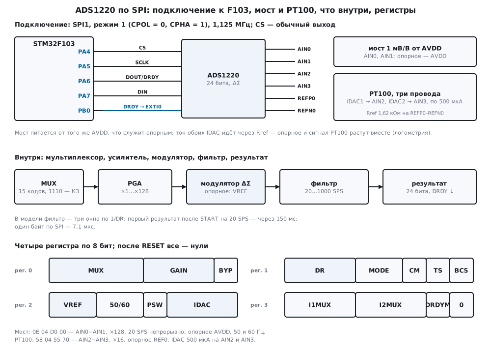
15г.2 Connecting it to the F103 and SPI mode 1
| ADS1220 pin | STM32F103 | Purpose |
|---|---|---|
| SCLK | PA5 | SPI1 clock |
| DIN | PA7 | MOSI: commands and data into the chip |
| DOUT/DRDY | PA6 | MISO: the reply; with DRDYM = 1 also "ready" |
| CS | PA4 | chip select, a plain output |
| DRDY | PB0 | "ready", EXTI0 on the falling edge |
| AVDD, DVDD, AVSS | 3.3 V and ground | ground shared with the microcontroller |
Without remap SPI1 sits on PA4–PA7 (RM0008, p. 185). By table 25 (p. 166) the master's SCK and MOSI are alternate function push-pull, MISO is an input, and NSS under software control is a plain pin. PA4–PA7 and PB0 do not tolerate 5 V (DocID13587, p. 29) — the ADS1220 is powered from 3.3 V.
The SPI mode is 1: the clock idles low, data are read on the falling edge
(18.2). Klipper opens its bus to the ADS1220 in exactly mode 1. The speed is
72 MHz / 64 = 1.125 MHz (BR = 101, p. 743), one byte takes 7.1 µs.
Klipper uses 256 or 512 kHz; we did not check 1.125 MHz with the chip, the
clock limit comes from the manufacturer's documentation. If in doubt,
BR = 111 gives 281 kHz.
static void spi1_init(void)
{
    RCC->APB2ENR |= RCC_APB2ENR_IOPAEN | RCC_APB2ENR_IOPBEN | RCC_APB2ENR_AFIOEN | RCC_APB2ENR_SPI1EN;
    RCC->AHBENR |= RCC_AHBENR_DMA1EN;
    GPIOA->BSRR = 1u << 4;                              /* CS вверх до настройки вывода */
    /* PA4 — выход 50 МГц (0011), PA5 и PA7 — альтернативная функция push-pull (1011), PA6 — вход (0100) */
    GPIOA->CRL = (GPIOA->CRL & 0x0000FFFFu) | 0xB4B30000u;
    GPIOB->CRL = (GPIOB->CRL & ~0xFu) | 0x8u;           /* PB0 — вход с подтяжкой (1000) */
    GPIOB->BSRR = 1u << 0;
    SPI1->CR1 = SPI_CR1_MSTR | SPI_CR1_CPHA | SPI_CR1_BR_2 | SPI_CR1_BR_0 | SPI_CR1_SSM | SPI_CR1_SSI;  /* режим 1, /64 */
    SPI1->CR2 = SPI_CR2_RXDMAEN | SPI_CR2_TXDMAEN;
    SPI1->CR1 |= SPI_CR1_SPE;
}
We drive CS ourselves (18.4): a command and its data must go in one
frame (15г.7). Before raising CS we wait for BSY = 0 (18.5). DRDY is on
PB0: AFIO_EXTICR1, bits 3:0 = 0001 — port B (p. 190), the falling edge is
enabled in EXTI_FTSR (p. 211).
15г.3 Commands and four registers
A command is one byte in a CS frame:
| Byte | Command | What it does |
|---|---|---|
| 0x06 | RESET | all registers to zero, conversion stopped |
| 0x08 | START/SYNC | start a conversion (or start it again) |
| 0x02 | POWERDOWN | stop and sleep |
| 0x10 | RDATA | the next three bytes are the result |
| 0x20 | rr << 2 | nn | RREG | read nn + 1 bytes from register rr |
| 0x40 | rr << 2 | nn | WREG | write nn + 1 bytes from register rr |
There are four registers, one byte each. After RESET all four are zero (Klipper checks them that way too).
| Reg. | Bits | Field | What it sets |
|---|---|---|---|
| 0 | 7:4 | MUX |
0000…0111 — the pairs AIN0−AIN1, AIN0−AIN2, AIN0−AIN3, AIN1−AIN2, AIN1−AIN3, AIN2−AIN3, AIN1−AIN0, AIN3−AIN2; 1000…1011 — AIN0…AIN3 against AVSS; 1100 — (REFP − REFN) / 4; 1101 — (AVDD − AVSS) / 4; 1110 — inputs shorted to (AVDD + AVSS) / 2 |
| 0 | 3:1 | GAIN |
000…111 — 1, 2, 4, 8, 16, 32, 64, 128 |
| 0 | 0 | PGA_BYPASS |
1 — bypass the amplifier; works only at gain 1, 2, 4 |
| 1 | 7:5 | DR |
000…110 — 20, 45, 90, 175, 330, 600, 1000 SPS; in turbo 40, 90, 180, 350, 660, 1200, 2000 |
| 1 | 4:3 | MODE |
00 — normal, 01 — duty-cycle, 10 — turbo |
| 1 | 2 | CM |
0 — single-shot, 1 — continuous |
| 1 | 1, 0 | TS, BCS |
temperature sensor instead of the inputs; burn-out current sources |
| 2 | 7:6 | VREF |
00 — its own 2.048 V, 01 — REFP0 − REFN0, 10 — REFP1 − REFN1 (these are AIN0 and AIN3), 11 — AVDD − AVSS |
| 2 | 5:4 | 50/60 |
00 — none, 01 — 50 and 60 Hz, 10 — 50 Hz, 11 — 60 Hz |
| 2 | 3 | PSW |
switch to AVSS — to cut the bridge supply |
| 2 | 2:0 | IDAC |
000 — off, 001…111 — 10, 50, 100, 250, 500, 1000, 1500 µA |
| 3 | 7:5, 4:2 | I1MUX, I2MUX |
where the current goes: 000 — nowhere, 001…100 — AIN0…AIN3, 101 — REFP0, 110 — REFN0 |
| 3 | 1 | DRDYM |
1 — "ready" also on DOUT/DRDY |
The MUX, GAIN, PGA_BYPASS, DR, MODE, CM and VREF fields and the MUX 0000–1011, gain, rate and reference codes match Klipper; Klipper also says that REF1 occupies AIN0 and AIN3 and that the amplifier cannot be bypassed at gains 8…128. The rest is from the manufacturer's documentation.
Reset and setup are done as in Klipper: after RESET read four zeros, after WREG read the registers back and compare.
/* RESET, пауза, и все четыре регистра должны прочитаться нулями */
int ads_reset(ads_t *d)
{
    uint8_t r[4];
    ads_cmd(d, ADS_CMD_RESET);
    ads_port_delay_us(ADS_RESET_US);
    ads_rreg(d, 0, r, 4);
    for (uint32_t i = 0; i < 4u; i++) {
        d->cfg[i] = 0;
        if (r[i])
            return ADS_E_RESET;
    }
    return ADS_OK;
}

/* записать четыре регистра одним WREG и прочитать обратно — как делает Klipper */
int ads_config(ads_t *d, const uint8_t cfg[4])
{
    uint8_t r[4];
    ads_wreg(d, 0, cfg, 4);
    ads_rreg(d, 0, r, 4);
    for (uint32_t i = 0; i < 4u; i++) {
        d->cfg[i] = cfg[i];
        if (r[i] != cfg[i])
            return ADS_E_VERIFY;
    }
    return ADS_OK;
}
In the model the reset — RESET 0x06, a 50 µs pause and RREG
23 00 00 00 00 answered by 00 00 00 00 after a junk byte — took
92.7 µs. The bridge setup is the WREG frame 43 0E 04 D0 00, read back as
0E 04 D0 00; the PT100 one is 43 58 04 55 70. The model assembled the
same bytes from the table fields independently of the driver. One byte at
1.125 MHz is 7.111 µs; a command is 7.1 µs, the three result bytes without
a command 21.3 µs, RDATA with the result 28.4 µs, WREG of all four
registers 35.6 µs.
15г.4 The result: 24 bits, volts, DRDY and the DMA stream
The result is three bytes, the most significant first, in two's
complement. The sign of bit 24 has to be extended into the upper bits of
an int32_t:
/* 24 бита в дополнительном коде, старший байт первым → int32_t */
int32_t ads_s24(const uint8_t b[3])
{
    int32_t v = (int32_t)((uint32_t)b[0] << 16 | (uint32_t)b[1] << 8 | b[2]);
    return v & 0x800000 ? v - 0x1000000 : v;
}

/* RDATA и три байта результата — в одном кадре */
int ads_read_data(ads_t *d, int32_t *code)
{
    uint8_t tx[4] = {ADS_CMD_RDATA, 0, 0, 0}, rx[4];
    ads_frame(d, tx, rx, 4);
    *code = ads_s24(rx + 1);
    return range(*code);
}

/* после спада DRDY результат выдвигается сам: 24 такта без команды, на DIN — нули */
int ads_read_direct(ads_t *d, int32_t *code)
{
    uint8_t tx[3] = {0, 0, 0}, rx[3];
    ads_frame(d, tx, rx, 3);
    *code = ads_s24(rx);
    return range(*code);
}
Klipper does the same — an OR with 0xFF000000 when bit 0x800000 is set. Without it a negative number becomes a huge positive one:
| Bytes | ads_s24 |
As an unsigned uint32_t |
|---|---|---|
| 7F FF FF | 8 388 607 | 8 388 607 |
| FF FF FF | −1 | 16 777 215 |
| FF FC 18 | −1000 | 16 776 216 |
| 80 00 00 | −8 388 608 | 8 388 608 |
Two ways to read. RDATA is the command and 24 clocks in one frame; it works at any moment. Without a command: after DRDY falls the result shifts out by itself — 24 clocks with zeros on DIN; this is how Klipper reads. Without the command the frame is shorter — 21.3 µs against 28.4.
Single-shot (CM = 0): START, wait for DRDY to fall, RDATA.
Continuous (CM = 1): one START, then every fall of DRDY is a new
result.
Into volts. Input = code × VREF / (gain × 2²³). The gain is a power of two, so the division is a shift:
int32_t ads_ratio(int32_t code, uint32_t scale, uint32_t gain)
{
    uint32_t sh = 23u + (gain & 7u);
    int64_t x = (int64_t)code * scale;
    int64_t half = (int64_t)1 << (sh - 1u);
    return (int32_t)(x >= 0 ? (x + half) >> sh : -((-x + half) >> sh));
}
scale is the reference in microvolts, and the result is microvolts at the
input; for the bridge and the PT100 the same call gives a ratio (15г.6). In
the model — the internal 2.048 V, single-shot at 1000 SPS:
| Gain | Range | One code | +1 mV: code | −1 mV: code | +10 mV: code |
|---|---|---|---|---|---|
| 1 | ±2048 mV | 244.1406 nV | 4145 | −4047 | 41 009 |
| 8 | ±256 mV | 30.5176 nV | 33 161 | −32 375 | 328 073 |
| 32 | ±64 mV | 7.6294 nV | 132 645 | −129 499 | 1 312 293 |
| 128 | ±16 mV | 1.9073 nV | 530 579 | −517 997 | 5 249 171 |
Back through ads_ratio this gave 1012 µV, −988 µV and 10 012 µV at any
gain: the model has an offset of +12 µV at the input (15г.6). The extreme
codes are ±2 048 000 µV. MUX = 1101 measures (AVDD − AVSS) / 4 with the
amplifier bypassed: at 3.3 V — code 3 379 249, 825 012 µV, that is
AVDD = 3 300 048 µV. This checks the supply without an extra wire.
DRDY into an interrupt, the result by DMA. In continuous mode there is
nothing to poll: the fall of DRDY raises EXTI0, the handler pulls CS
down and starts DMA for three bytes (channel 2 — SPI1_RX, channel 3 —
SPI1_TX, table 78, p. 281), and the end of reception raises CS and
puts the sample into a ring. The CPU takes no part in the transfer.
/* приём — канал 2 (SPI1_RX), передача — канал 3 (SPI1_TX); приём включается первым */
void ads_port_dma_start(const uint8_t *tx, uint8_t *rx, uint32_t n)
{
    DMA1_Channel2->CCR = 0;
    DMA1_Channel3->CCR = 0;
    DMA1->IFCR = DMA_IFCR_CGIF2 | DMA_IFCR_CGIF3;
    DMA1_Channel2->CPAR = (uint32_t)&SPI1->DR;
    DMA1_Channel2->CMAR = (uint32_t)rx;
    DMA1_Channel2->CNDTR = n;
    DMA1_Channel2->CCR = DMA_CCR2_MINC | DMA_CCR2_TCIE | DMA_CCR2_EN;
    DMA1_Channel3->CPAR = (uint32_t)&SPI1->DR;
    DMA1_Channel3->CMAR = (uint32_t)tx;
    DMA1_Channel3->CNDTR = n;
    DMA1_Channel3->CCR = DMA_CCR3_MINC | DMA_CCR3_DIR | DMA_CCR3_EN;
}

/* DRDY: спад на PB0 */
void EXTI0_IRQHandler(void)
{
    EXTI->PR = 1u << 0;
    if (streaming)
        ads_on_drdy(&adc);                              /* CS вниз и DMA на три байта */
    else
        drdy = 1;
}

/* приняты все три байта: последний бит уже на месте, BSY не ждём */
void DMA1_Channel2_IRQHandler(void)
{
    DMA1->IFCR = DMA_IFCR_CGIF2 | DMA_IFCR_CGIF3;
    DMA1_Channel2->CCR = 0;
    DMA1_Channel3->CCR = 0;
    ads_on_dma_done(&adc);                              /* CS вверх, отсчёт — в кольцо */
}

void ads_on_drdy(ads_t *d)
{
    if (d->dma_busy) {                                  /* прошлый отсчёт ещё не дочитан */
        d->overruns++;
        return;
    }
    d->dma_busy = 1;
    ads_port_cs(0);
    ads_port_dma_start(d->dma_tx, d->dma_rx, 3);
}

void ads_on_dma_done(ads_t *d)
{
    ads_port_cs(1);
    d->ring[d->head % ADS_RING] = ads_s24(d->dma_rx);
    d->head++;
    d->frames++;
    d->bytes += 3;
    d->dma_busy = 0;
}
Reception is enabled before transmission: otherwise the first byte would
leave with nobody to receive it. TXDMAEN and RXDMAEN (p. 745) are set
once during setup. In the model at 2000 SPS (turbo) 2000 samples arrived in
1 001 028.4 µs — 2001 frames (START and 2000 of three bytes), 6001 bytes,
not a single miss. Reading a sample occupies the bus for 21.33 µs out of
500 — 4.3 %. If the end of DMA comes later than the next fall (in the
model after 600 µs with a period of 500), ads_on_drdy sees DMA busy and
counts an overrun: 100 overruns for 100 samples read, 99 results lost.
DRDYM. If there is no free pin for DRDY, DRDYM = 1 puts "ready" on
DOUT/DRDY while CS is low: ads_wait_dout pulls CS down, waits for a
zero on MISO (PA6 is a plain input, its level is visible in IDR) and
shifts out the 24 bits at once — in the model one frame, three bytes.
With DRDYM = 0 the pin does not show "ready", and in the model the
function returned ADS_E_TIMEOUT.
15г.5 The filter: data rate, settling time, 50/60 Hz, turbo
A delta-sigma converter gives not an instantaneous value but the average over the filter window. In the model the filter is three averaging windows in a row of 1/DR each (sinc3); according to the manufacturer's documentation the real filter of the chip is more complex, and its times are in the manufacturer's table, not checked. Three things follow from such a filter.
The first result after START comes after the whole window, not after 1/DR. Single-shot in the model, from START to the end of RDATA:
| Mode | Rate | 1/DR | Filter window | Single-shot |
|---|---|---|---|---|
| normal | 20 SPS | 50 000 µs | 150 000 µs | 150 035.6 µs |
| normal | 45 SPS | 22 222.2 µs | 66 666.7 µs | 66 702.2 µs |
| normal | 90 SPS | 11 111.1 µs | 33 333.3 µs | 33 368.9 µs |
| normal | 175 SPS | 5714.3 µs | 17 142.9 µs | 17 178.4 µs |
| normal | 330 SPS | 3030.3 µs | 9090.9 µs | 9126.5 µs |
| normal | 600 SPS | 1666.7 µs | 5000 µs | 5035.6 µs |
| normal | 1000 SPS | 1000 µs | 3000 µs | 3035.6 µs |
| turbo | 40 SPS | 25 000 µs | 75 000 µs | 75 035.6 µs |
| turbo | 2000 SPS | 500 µs | 1500 µs | 1535.6 µs |
The 35.6 µs above the window are START (7.1 µs) and RDATA (28.4 µs). Changing the input or the reference is the same: in the model a register write in continuous mode restarts the conversion, and the next result comes after a whole window. Two channels in turn at 20 SPS take 150 ms per channel, not 50.
After a step at the input — three results. Continuous mode, the input jumps from zero to the full bridge load right after the first result; the share of the step in each next one:
| Where in the period | 1st | 2nd | 3rd | 4th | 5th |
|---|---|---|---|---|---|
| at the very start | 0 % | 16.7 % | 83.3 % | 100 % | 100 % |
| in the middle | 0 % | 2.1 % | 50 % | 97.9 % | 100 % |
The same at 20 and 1000 SPS and in turbo: what counts is the number of periods, not the time. A scale that must show a new load needs three results after the load has settled.
Mains at 50 and 60 Hz. A window that is a whole number of hum periods long cancels it completely. Hum of 1 mV amplitude in the bridge difference, gain 128, 32 results in a row, the largest deviation:
| Rate | 50 Hz | 60 Hz |
|---|---|---|
| 20 SPS, 50/60 = 00 | 0.93 µV | 0 |
| 45 SPS | 0.93 µV | 7.85 µV |
| 90 SPS | 178.4 µV | 62.8 µV |
| 175 SPS | 660.7 µV | 546.2 µV |
| 330 SPS | 892.1 µV | 844.2 µV |
| 600 SPS | 946.4 µV | 939 µV |
| 1000 SPS | 987.7 µV | 981.7 µV |
| 20 SPS, 50/60 = 01 (both) | 0 | 0 |
| 20 SPS, 50/60 = 10 (50 Hz) | 0 | 0 |
| 20 SPS, 50/60 = 11 (60 Hz) | 3.09 µV | 0 |
| turbo 40 SPS, 50/60 = 00 or 01 | 5.54 µV | 4.39 µV |
According to the manufacturer's documentation the 50/60 field acts only
at 20 SPS in normal mode, and at other rates the model ignores it. How it
is built inside the chip was not checked; in the model one of the three
windows is replaced by a 20 ms window (50 Hz) or a 16.667 ms window
(60 Hz), and the single-shot window became 86 666.7 µs (01), 120 000 µs
(10) or 116 666.7 µs (11). At 1000 SPS the hum passes almost entirely —
987.7 µV out of 1000. If speed is needed, the hum is removed in software:
the average of 20 consecutive results at 1000 SPS — exactly 20 ms — left 0
in the model.
Turbo (MODE = 10) — the internal clock is twice as fast (Klipper says
so too), the rate for the same DR codes is twice as high. 40 SPS in turbo
is not 20 SPS: the 50/60 filter does not work, 5.54 µV remain. And the
noise grows with the rate: below is the bridge with noise.
Noise. In the model the noise at the chip input is 0.08 µV × √(DR / 20), the bridge adds its own 0.05 µV × √(DR / 20) (model assumptions, not data from a document). A 1 mV/V bridge for 5 kg, AVDD 3.3 V, gain 128 — 214.75 codes per gram; 400 results each:
| Rate | Noise, codes | Noise, nV | Noise, g |
|---|---|---|---|
| 20 SPS | 29 | 89.2 | 0.135 |
| 90 SPS | 66.4 | 204.1 | 0.309 |
| 330 SPS | 119.4 | 366.8 | 0.556 |
| 1000 SPS | 229.3 | 704.9 | 1.068 |
Twenty-four bits do not mean 24 bits of accuracy: at 20 SPS the five lowest bits are noise. For a scale — 20 SPS with the 50/60 filter, which handles both the mains and the noise.
15г.6 Ratiometric measurement: the bridge and the PT100, IDAC currents, offset calibration
The bridge from the same reference. The bridge is powered from AVDD,
and the reference is AVDD (VREF = 11): the bridge signal and the
reference grow together, and the code does not depend on AVDD. In the
model, a 1 mV/V bridge, single-shot at 20 SPS with 50/60:
| Reference | AVDD | No load | Half | Full | Full − no load |
|---|---|---|---|---|---|
| AVDD | 3.0 V | 4295 | 541 166 | 1 078 037 | 1 073 742 |
| AVDD | 3.3 V | 3905 | 540 775 | 1 077 646 | 1 073 741 |
| AVDD | 3.6 V | 3579 | 540 450 | 1 077 321 | 1 073 742 |
| its own 2.048 V | 3.0 V | 6291 | 792 723 | 1 579 155 | 1 572 864 |
| its own 2.048 V | 3.3 V | 6291 | 871 367 | 1 736 442 | 1 730 151 |
| its own 2.048 V | 3.6 V | 6291 | 950 010 | 1 893 728 | 1 887 437 |
With AVDD as the reference the span does not change — ±1 code for ±9 % of
supply. With its own 2.048 V it follows the supply one to one: at 3.6 V the
scale shows 9.1 % more. The no-load code is the offset (below).
ads_ratio(code, 1 000 000 000, ×128) gives the ratio in nV per volt of
supply: no load — 3637 nV/V, full — 1 003 636 nV/V, difference —
999 999 nV/V, that is 1 mV/V. Grams come from this by tare and a known
load, 102.6.
If the bridge is far away and the supply wires are long, their drop also
goes into the result. Then the reference is taken right at the bridge by a
separate pair to REFP0/REFN0 (VREF = 01) — this is a six-wire load cell;
not checked in the model.
A three-wire PT100. The current for the thermometer comes from the chip
itself: IDAC = 101 — 500 µA, IDAC1 goes to AIN2, IDAC2 to AIN3 (I1MUX =
011, I2MUX = 100). IDAC1 flows down wire L1 through the PT100, IDAC2
down wire L2 to the lower PT100 terminal; both meet in the third wire and
go through Rref = 1.62 kΩ to ground. The input is AIN2 − AIN3 (MUX =
0101), the reference is the drop across Rref, REFP0 − REFN0 (VREF = 01):
- difference = I1 · (R + L1) − I2 · L2 = I · R if the currents and wires are equal;
- reference = (I1 + I2) · Rref = 2 · I · Rref;
- code / (gain × 2²³) = R / (2 · Rref), R = code × 2 · Rref / (gain × 2²³).
The current does not enter the result — this is the same ratiometric measurement as in 176б.3, only the divider is replaced by current sources. Wires L1 and L2 cancel — the same three-wire scheme as in 176б.4. Rref at the bottom lifts both inputs: at 200 °C in the model AIN2 = 1.7086 V, AIN3 = 1.6205 V, REFP0 = 1.62 V, common mode 1.6646 V, difference 88.105 mV with a range of ±101.25 mV (1.62 V / 16) — the amplifier stays within its limits (below, 15г.7).
/* PT100 по трём проводам: среднее с токами как есть и с переставленными I1MUX и I2MUX */
int ads_rtd3(ads_t *d, uint32_t n, int32_t out[3])
{
    uint8_t keep = d->cfg[3];
    uint8_t swap = (uint8_t)((keep >> ADS_I1MUX_POS & 7u) << ADS_I2MUX_POS | (keep >> ADS_I2MUX_POS & 7u) << ADS_I1MUX_POS
                             | (keep & 3u));
    int rc = ads_average(d, n, &out[0]);
    if (rc == ADS_OK)
        rc = ads_set(d, 3, swap);
    if (rc == ADS_OK)
        rc = ads_average(d, n, &out[1]);
    int rc2 = ads_set(d, 3, keep);
    int64_t s = (int64_t)out[0] + out[1];
    out[2] = (int32_t)(s >= 0 ? (s + 1) / 2 : -((-s + 1) / 2));
    return rc != ADS_OK ? rc : rc2;
}
The model compared the REF0 reference with the internal 2.048 V (gain 8, R by Ohm's law with the nominal 500 µA) when both currents are ±1 % off nominal:
| T | R, mΩ | REF0: −1 % / 0 / +1 % | its own 2.048 V: −1 % / 0 / +1 % |
|---|---|---|---|
| 0 °C | 100 000 | 100 024 / 100 024 / 100 024 | 99 024 / 100 024 / 101 024 |
| 100 °C | 138 505 | 138 530 / 138 530 / 138 529 | 137 144 / 138 530 / 139 914 |
| 200 °C | 175 856 | 175 880 / 175 880 / 175 880 | 174 122 / 175 880 / 177 638 |
With REF0 the current does not matter at all. With its own reference 1 % of current is ±1 Ω at 0 °C, about 2.6 °C. The constant +24 mΩ is the 12 µV offset at 0.5 mA.
Mismatch of the two currents. If IDAC1 and IDAC2 differ, the wires do
not cancel completely, and the current difference is multiplied by R.
ads_rtd3 measures twice — with the currents as they are and with
I1MUX/I2MUX swapped — and takes the average: the difference goes
away. In the model, 100 °C, wires of 0.35 Ω each, four results per
measurement:
| Case | As is | Swapped | Average |
|---|---|---|---|
| equal currents | 138 530 mΩ, 0.0646 °C | 138 530 mΩ | 138 530 mΩ, 0.0646 °C |
| currents differ by 0.4 % | 138 808 mΩ, 0.7976 °C | 138 251 mΩ, −0.671 °C | 138 530 mΩ, 0.0646 °C |
| equal currents, L1 5 % longer | 138 547 mΩ, 0.1094 °C | 138 547 mΩ | 138 547 mΩ, 0.1094 °C |
A 0.4 % mismatch is almost 0.8 °C, the swap removes it completely. Unequal wires are not cured by the swap: +17 mΩ, 0.0448 °C on top of the offset — exactly as much as in 176б.4. The 0.0646 °C in every row is the offset; calibration removes it.
Offset calibration. MUX = 1110 shorts both inputs to
(AVDD + AVSS) / 2: whatever the chip shows then is its offset. Measure it
with the same gain and at the same rate as the signal.
/* смещение: MUX = 1110 замыкает входы на (AVDD + AVSS) / 2; усиление то же, что у измерения */
int ads_offset(ads_t *d, uint32_t n, int32_t *off)
{
    uint8_t keep = d->cfg[0];
    int rc = ads_set(d, 0, (uint8_t)(ADS_SHORT << ADS_MUX_POS | (keep & 0x0Fu)));
    if (rc == ADS_OK)
        rc = ads_average(d, n, off);
    int rc2 = ads_set(d, 0, keep);
    return rc != ADS_OK ? rc : rc2;
}
In the model (offset +12 µV, noise on) the unloaded bridge gave an average
of 3894 codes over 16 results — 18.13 g on an empty scale. ads_offset
over 16 results — 3914 codes, 12.029 µV; the registers returned to
0E 04 D0 00. After subtraction eight averages of 16 lie between −16 and
3 codes, less than 0.075 g. This is not tare: tare removes both the offset
and the initial bridge imbalance (102.6), while calibration with MUX =
1110 removes only the ADC part, but without unloading the scale, at any
time and for the PT100 too.
15г.7 Pitfalls
No pause after RESET. Klipper says the reset takes 50 µs. At 1.125 MHz
the RESET command ends after 7.1 µs, and a WREG right after it lands in the
deaf time. In the model all five WREG bytes were lost, and 100 µs later
the registers read 00 00 00 00 instead of 0E 04 D0 00. With the
ADS_RESET_US pause the setup went through and was verified.
CS raised in the middle of a command. Raising CS aborts the
command. RREG in one frame and the zeros for the reply in another: in the
model 00 00 00 00 came back. The three result bytes with a frame per
byte: only the top byte was read — 524 288 (0x080000) instead of 540 775
(0x084067). A frame is one command with all its data (ads_frame).
Whether the chip behaves like this in the second and third frame was not
checked; in the model DOUT gives zeros when it has no data.
Input outside the amplifier in common mode. With the PGA on, the outputs Vcm ± gain × Vd / 2 must stay between AVSS + 0.2 V and AVDD − 0.2 V (manufacturer's documentation). A 5 mV difference at gain 128 — common-mode limits from 0.52 to 2.78 V:
| Common mode | Code | Shown |
|---|---|---|
| 1.65 V | 2 627 731 | 5012 µV |
| 0.60 V | 2 627 731 | 5012 µV |
| 0.45 V | 2 341 011 | 4465 µV |
| 0.30 V | 1 726 611 | 3293 µV |
| 0.10 V | 907 411 | 1731 µV |
No error, no flag — just a wrong number. An input against AVSS is the same
case: 5 mV on AIN0 against AVSS at gain 128 showed 969 µV, at gain 4 with
the PGA on — 12 µV (the offset alone), at gain 4 with PGA_BYPASS = 1 —
5012 µV. That is why Klipper forces the PGA bypass for an input against
AVSS. The bridge from AVDD sits at AVDD / 2, the PT100 is lifted by Rref —
they do not have this problem.
Turbo instead of normal. DR = 000 in turbo is 40 SPS, not 20, and the
50/60 field does not act: 5.54 µV of 50 Hz hum instead of zero (15г.5).
ads_sps takes the mode into account; a rate table without MODE does
not.
SPI in mode 0. The chip reads DIN on the falling edge, and a master in
mode 0 also changes data on the falling edge — commands get through. But
the master latches the reply one clock early (18.2): in the model the check
after RESET passed — zeros cannot be spoiled by a shift — while the setup
returned 07 02 68 00 instead of 0E 04 D0 00 and ADS_E_VERIFY. Mode 1:
CPHA = 1.
The result as a uint32_t. −1 mV at gain 128 is code −517 997
(0xF81893); without sign extension it is 16 259 219 (15г.4).
Hitting the edge. 20 mV on a ±16 mV range is code 8 388 607, and
ads_read_data returned ADS_E_RANGE: the edge of the range is not a
measurement.
Reading too late. A sample not read by the next fall of DRDY is lost; in the model, with the end of DMA after 600 µs at 2000 SPS — 100 overruns for 100 samples (15г.4).
15г.8 Summary
- The ADS1220 — 24 bits, gain 1…128, four inputs and three service combinations, reference its own 2.048 V, REF0, REF1 or AVDD, 20…1000 SPS (turbo 40…2000), two current sources up to 1500 µA; SPI in mode 1.
- Commands: RESET 0x06, START 0x08, POWERDOWN 0x02, RDATA 0x10, RREG 0x20, WREG 0x40; after RESET a 50 µs pause and four zeros; after WREG read back.
- The result is an
int32_tfrom three bytes with sign extension; input = code × VREF / (gain × 2²³), at 2.048 V and ×128 — 1.9073 nV per code. - The first result comes after the filter window: 150 035.6 µs at 20 SPS in the model; after a step — the third result; a channel at 20 SPS — 150 ms.
- At 1000 SPS 50 Hz passes almost entirely (987.7 µV out of 1000); 20 SPS with 50/60 = 01 — 0; in turbo the field does not work.
- A bridge from AVDD with AVDD as the reference: span 1 073 741 ± 1 code over 3.0–3.6 V; with its own reference — plus 9.1 % at 3.6 V.
- PT100: two IDACs of 500 µA, Rref on REF0, R = code × 2 · Rref / (gain × 2²³); swapping the currents removes 0.8 °C of mismatch.
MUX= 1110 — the offset: 3914 codes instead of 18.13 g on an empty scale.- DRDY on EXTI0, three bytes by DMA: 2000 SPS without misses, the bus busy 4.3 %.
Full sources
ads15e.h — commands, the fields of the four registers, codes, the port and the driver functions.
/* ads15e.h — раздел 15г: драйвер внешнего 24-битного АЦП ADS1220 по SPI без регистров микроконтроллера.
 * Драйвер говорит с микросхемой только через функции порта (ads_port_*): в прошивке fw15e.c их делают
 * SPI1, EXTI0 и DMA1 STM32F103, в стенде bench15e.c — модель model15e.py.
 * Коды команд RESET, START/SYNC, RREG, WREG, раскладка полей MUX, GAIN, PGA_BYPASS, DR, MODE, CM, VREF,
 * значения после сброса и скорости сверены с драйвером Klipper (klippy/extras/ads1220.py); остальное —
 * по документации производителя, документа в проекте нет, с микросхемой не сверено. */
#ifndef ADS15E_H
#define ADS15E_H
#include <stdint.h>

/* ── команды: один байт в кадре CS ─────────────────────────────────────── */
#define ADS_CMD_POWERDOWN 0x02u
#define ADS_CMD_RESET     0x06u
#define ADS_CMD_START     0x08u         /* START/SYNC: начать (заново) преобразование */
#define ADS_CMD_RDATA     0x10u         /* следующие три байта — результат */
#define ADS_CMD_RREG      0x20u         /* 0010 rrnn: с регистра rr, nn + 1 байт */
#define ADS_CMD_WREG      0x40u         /* 0100 rrnn */

/* ── регистр 0 ───────────────────────────────────────────────────────── */
#define ADS_MUX_POS       4u            /* 7:4 — входы AINP и AINN */
#define ADS_GAIN_POS      1u            /* 3:1 — усиление 1…128 */
#define ADS_PGA_BYPASS    0x01u         /* обойти PGA: только при усилении 1, 2, 4 */
/* ── регистр 1 ───────────────────────────────────────────────────────── */
#define ADS_DR_POS        5u            /* 7:5 — скорость */
#define ADS_MODE_POS      3u            /* 4:3 — 00 нормальный, 01 экономичный, 10 turbo */
#define ADS_CM            0x04u         /* 1 — непрерывное преобразование */
#define ADS_TS            0x02u         /* датчик температуры вместо входов */
#define ADS_BCS           0x01u         /* токи 10 мкА для поиска обрыва */
/* ── регистр 2 ───────────────────────────────────────────────────────── */
#define ADS_VREF_POS      6u            /* 7:6 — опорное */
#define ADS_5060_POS      4u            /* 5:4 — подавление 50/60 Гц (только 20 SPS) */
#define ADS_PSW           0x08u         /* ключ на AVSS для питания моста */
#define ADS_IDAC_POS      0u            /* 2:0 — величина обоих токов возбуждения */
/* ── регистр 3 ───────────────────────────────────────────────────────── */
#define ADS_I1MUX_POS     5u            /* 7:5 — куда выведен IDAC1 */
#define ADS_I2MUX_POS     2u            /* 4:2 — куда выведен IDAC2 */
#define ADS_DRDYM         0x02u         /* «готово» ещё и на DOUT/DRDY */

enum { ADS_AIN0_AIN1, ADS_AIN0_AIN2, ADS_AIN0_AIN3, ADS_AIN1_AIN2, ADS_AIN1_AIN3, ADS_AIN2_AIN3,
       ADS_AIN1_AIN0, ADS_AIN3_AIN2, ADS_AIN0_AVSS, ADS_AIN1_AVSS, ADS_AIN2_AVSS, ADS_AIN3_AVSS,
       ADS_MON_REF4, ADS_MON_AVDD4, ADS_SHORT };        /* MUX 0000…1110; 1110 — входы закорочены */
enum { ADS_G1, ADS_G2, ADS_G4, ADS_G8, ADS_G16, ADS_G32, ADS_G64, ADS_G128 };   /* GAIN 000…111 */
enum { ADS_DR_20, ADS_DR_45, ADS_DR_90, ADS_DR_175, ADS_DR_330, ADS_DR_600, ADS_DR_1000 };  /* в turbo — вдвое */
enum { ADS_MODE_NORMAL, ADS_MODE_DUTY, ADS_MODE_TURBO };
enum { ADS_VREF_INT, ADS_VREF_REF0, ADS_VREF_REF1, ADS_VREF_AVDD };  /* 2,048 В; REFP0−REFN0; REFP1−REFN1; AVDD−AVSS */
enum { ADS_5060_OFF, ADS_5060_BOTH, ADS_5060_50, ADS_5060_60 };
enum { ADS_IDAC_OFF, ADS_IDAC_10, ADS_IDAC_50, ADS_IDAC_100, ADS_IDAC_250, ADS_IDAC_500, ADS_IDAC_1000,
       ADS_IDAC_1500 };                                  /* мкА */
enum { ADS_IMUX_OFF, ADS_IMUX_AIN0, ADS_IMUX_AIN1, ADS_IMUX_AIN2, ADS_IMUX_AIN3, ADS_IMUX_REFP0,
       ADS_IMUX_REFN0 };

#define ADS_CFG0(mux, g, byp)   ((uint8_t)((mux) << ADS_MUX_POS | (g) << ADS_GAIN_POS | (byp)))
#define ADS_CFG1(dr, mode, cm)  ((uint8_t)((dr) << ADS_DR_POS | (mode) << ADS_MODE_POS | (cm)))
#define ADS_CFG2(vref, f, idac) ((uint8_t)((vref) << ADS_VREF_POS | (f) << ADS_5060_POS | (idac)))
#define ADS_CFG3(i1, i2, drdym) ((uint8_t)((i1) << ADS_I1MUX_POS | (i2) << ADS_I2MUX_POS | (drdym)))

#define ADS_RESET_US      50u           /* после RESET микросхема глуха — пауза, как в Klipper */
#define ADS_TIMEOUT_US    200000u       /* дольше любого первого результата, с запасом */
#define ADS_RING          64u           /* кольцо отсчётов потока по DMA */

enum { ADS_OK = 0, ADS_E_TIMEOUT = -1, ADS_E_VERIFY = -2, ADS_E_RESET = -3, ADS_E_RANGE = -4 };

typedef struct {
    uint8_t cfg[4];                     /* что драйвер записал в регистры 0…3 */
    uint32_t frames, bytes;             /* кадров CS и байт по SPI */
    /* поток по DRDY и DMA: заполняют обработчики прерываний */
    uint8_t dma_tx[3], dma_rx[3];
    volatile uint8_t dma_busy;
    volatile uint32_t head, overruns;
    int32_t ring[ADS_RING];
} ads_t;

/* ── порт: в прошивке — SPI1, EXTI0 и DMA1, в стенде — строки к модели ─── */
void ads_port_cs(int level);                                     /* 0 — микросхема выбрана */
void ads_port_xfer(const uint8_t *tx, uint8_t *rx, uint32_t n);  /* n байт туда и обратно, CS не трогает */
void ads_port_delay_us(uint32_t us);
int ads_port_wait_drdy(uint32_t timeout_us);    /* спад DRDY (флаг EXTI) за timeout_us: 1 — был и снят */
int ads_port_miso(void);                        /* уровень DOUT/DRDY: нужен для DRDYM */
void ads_port_dma_start(const uint8_t *tx, uint8_t *rx, uint32_t n);   /* запустить и не ждать */

/* ── драйвер ──────────────────────────────────────────────────────────── */
void ads_frame(ads_t *d, const uint8_t *tx, uint8_t *rx, uint32_t n);
void ads_cmd(ads_t *d, uint8_t cmd);
void ads_wreg(ads_t *d, uint32_t reg, const uint8_t *v, uint32_t n);
void ads_rreg(ads_t *d, uint32_t reg, uint8_t *v, uint32_t n);
int ads_reset(ads_t *d);
int ads_config(ads_t *d, const uint8_t cfg[4]);
int ads_set(ads_t *d, uint32_t reg, uint8_t v);
int32_t ads_s24(const uint8_t b[3]);
int ads_read_data(ads_t *d, int32_t *code);
int ads_read_direct(ads_t *d, int32_t *code);
int ads_single(ads_t *d, int32_t *code);
int ads_next(ads_t *d, int32_t *code);
int ads_average(ads_t *d, uint32_t n, int32_t *mean);
int ads_offset(ads_t *d, uint32_t n, int32_t *off);
int ads_rtd3(ads_t *d, uint32_t n, int32_t out[3]);
int ads_wait_dout(ads_t *d, uint32_t timeout_us, int32_t *code);
uint32_t ads_sps(const ads_t *d);
int32_t ads_ratio(int32_t code, uint32_t scale, uint32_t gain);
void ads_stream_start(ads_t *d);
void ads_on_drdy(ads_t *d);
void ads_on_dma_done(ads_t *d);

#endif
ads15e.c — driver: frames, reset and setup, 24 bits, single-shot and continuous, offset, PT100, the stream.
/* ads15e.c — раздел 15г: драйвер ADS1220 по SPI. Один и тот же файл собирается в прошивку (armclang,
 * Cortex-M3) и в стенд (arm-none-eabi-gcc, QEMU): микроконтроллера он не знает, только порт ads_port_*. */
#include "ads15e.h"

static const uint16_t sps_normal[7] = {20, 45, 90, 175, 330, 600, 1000};   /* DR 000…110 */

/* один кадр: CS вниз, n байт туда и обратно, CS вверх — команда и её данные не разрываются */
void ads_frame(ads_t *d, const uint8_t *tx, uint8_t *rx, uint32_t n)
{
    ads_port_cs(0);
    ads_port_xfer(tx, rx, n);
    ads_port_cs(1);
    d->frames++;
    d->bytes += n;
}

void ads_cmd(ads_t *d, uint8_t cmd)
{
    uint8_t rx;
    ads_frame(d, &cmd, &rx, 1);
}

void ads_wreg(ads_t *d, uint32_t reg, const uint8_t *v, uint32_t n)
{
    uint8_t tx[5], rx[5];
    tx[0] = (uint8_t)(ADS_CMD_WREG | (reg & 3u) << 2 | ((n - 1u) & 3u));
    for (uint32_t i = 0; i < n; i++)
        tx[1 + i] = v[i];
    ads_frame(d, tx, rx, n + 1u);
}

void ads_rreg(ads_t *d, uint32_t reg, uint8_t *v, uint32_t n)
{
    uint8_t tx[5] = {(uint8_t)(ADS_CMD_RREG | (reg & 3u) << 2 | ((n - 1u) & 3u)), 0, 0, 0, 0}, rx[5];
    ads_frame(d, tx, rx, n + 1u);
    for (uint32_t i = 0; i < n; i++)
        v[i] = rx[1 + i];                               /* в ответ на байт команды пришёл мусор */
}

/* RESET, пауза, и все четыре регистра должны прочитаться нулями */
int ads_reset(ads_t *d)
{
    uint8_t r[4];
    ads_cmd(d, ADS_CMD_RESET);
    ads_port_delay_us(ADS_RESET_US);
    ads_rreg(d, 0, r, 4);
    for (uint32_t i = 0; i < 4u; i++) {
        d->cfg[i] = 0;
        if (r[i])
            return ADS_E_RESET;
    }
    return ADS_OK;
}

/* записать четыре регистра одним WREG и прочитать обратно — как делает Klipper */
int ads_config(ads_t *d, const uint8_t cfg[4])
{
    uint8_t r[4];
    ads_wreg(d, 0, cfg, 4);
    ads_rreg(d, 0, r, 4);
    for (uint32_t i = 0; i < 4u; i++) {
        d->cfg[i] = cfg[i];
        if (r[i] != cfg[i])
            return ADS_E_VERIFY;
    }
    return ADS_OK;
}

int ads_set(ads_t *d, uint32_t reg, uint8_t v)
{
    uint8_t r;
    ads_wreg(d, reg, &v, 1);
    ads_rreg(d, reg, &r, 1);
    d->cfg[reg & 3u] = v;
    return r == v ? ADS_OK : ADS_E_VERIFY;
}

/* 24 бита в дополнительном коде, старший байт первым → int32_t */
int32_t ads_s24(const uint8_t b[3])
{
    int32_t v = (int32_t)((uint32_t)b[0] << 16 | (uint32_t)b[1] << 8 | b[2]);
    return v & 0x800000 ? v - 0x1000000 : v;
}

static int range(int32_t code)
{
    return code == 0x7FFFFF || code == -0x800000 ? ADS_E_RANGE : ADS_OK;   /* упёрлись в край */
}

/* RDATA и три байта результата — в одном кадре */
int ads_read_data(ads_t *d, int32_t *code)
{
    uint8_t tx[4] = {ADS_CMD_RDATA, 0, 0, 0}, rx[4];
    ads_frame(d, tx, rx, 4);
    *code = ads_s24(rx + 1);
    return range(*code);
}

/* после спада DRDY результат выдвигается сам: 24 такта без команды, на DIN — нули */
int ads_read_direct(ads_t *d, int32_t *code)
{
    uint8_t tx[3] = {0, 0, 0}, rx[3];
    ads_frame(d, tx, rx, 3);
    *code = ads_s24(rx);
    return range(*code);
}

/* однократное (CM = 0): START, спад DRDY, RDATA */
int ads_single(ads_t *d, int32_t *code)
{
    (void)ads_port_wait_drdy(0);                        /* снять старый флаг */
    ads_cmd(d, ADS_CMD_START);
    if (!ads_port_wait_drdy(ADS_TIMEOUT_US))
        return ADS_E_TIMEOUT;
    return ads_read_data(d, code);
}

/* непрерывное (CM = 1): следующий результат по спаду DRDY */
int ads_next(ads_t *d, int32_t *code)
{
    if (!ads_port_wait_drdy(ADS_TIMEOUT_US))
        return ADS_E_TIMEOUT;
    return ads_read_direct(d, code);
}

int ads_average(ads_t *d, uint32_t n, int32_t *mean)
{
    int64_t sum = 0;
    int32_t c;
    for (uint32_t i = 0; i < n; i++) {
        int rc = d->cfg[1] & ADS_CM ? ads_next(d, &c) : ads_single(d, &c);
        if (rc != ADS_OK)
            return rc;
        sum += c;
    }
    *mean = (int32_t)(sum >= 0 ? (sum + n / 2u) / n : -((-sum + n / 2u) / n));
    return ADS_OK;
}

/* смещение: MUX = 1110 замыкает входы на (AVDD + AVSS) / 2; усиление то же, что у измерения */
int ads_offset(ads_t *d, uint32_t n, int32_t *off)
{
    uint8_t keep = d->cfg[0];
    int rc = ads_set(d, 0, (uint8_t)(ADS_SHORT << ADS_MUX_POS | (keep & 0x0Fu)));
    if (rc == ADS_OK)
        rc = ads_average(d, n, off);
    int rc2 = ads_set(d, 0, keep);
    return rc != ADS_OK ? rc : rc2;
}

/* PT100 по трём проводам: среднее с токами как есть и с переставленными I1MUX и I2MUX */
int ads_rtd3(ads_t *d, uint32_t n, int32_t out[3])
{
    uint8_t keep = d->cfg[3];
    uint8_t swap = (uint8_t)((keep >> ADS_I1MUX_POS & 7u) << ADS_I2MUX_POS | (keep >> ADS_I2MUX_POS & 7u) << ADS_I1MUX_POS
                             | (keep & 3u));
    int rc = ads_average(d, n, &out[0]);
    if (rc == ADS_OK)
        rc = ads_set(d, 3, swap);
    if (rc == ADS_OK)
        rc = ads_average(d, n, &out[1]);
    int rc2 = ads_set(d, 3, keep);
    int64_t s = (int64_t)out[0] + out[1];
    out[2] = (int32_t)(s >= 0 ? (s + 1) / 2 : -((-s + 1) / 2));
    return rc != ADS_OK ? rc : rc2;
}

/* DRDYM = 1: «готово» — ноль на DOUT/DRDY при выбранной микросхеме; отдельный провод DRDY не нужен */
int ads_wait_dout(ads_t *d, uint32_t timeout_us, int32_t *code)
{
    uint8_t tx[3] = {0, 0, 0}, rx[3];
    ads_port_cs(0);
    for (uint32_t t = 0; ads_port_miso(); t += 10u) {
        if (t >= timeout_us) {
            ads_port_cs(1);
            return ADS_E_TIMEOUT;
        }
        ads_port_delay_us(10);
    }
    ads_port_xfer(tx, rx, 3);
    ads_port_cs(1);
    d->frames++;
    d->bytes += 3;
    *code = ads_s24(rx);
    return range(*code);
}

/* скорость по DR и MODE: в turbo вдвое; экономичный режим здесь не разбирается — 0 */
uint32_t ads_sps(const ads_t *d)
{
    uint32_t dr = d->cfg[1] >> ADS_DR_POS & 7u, mode = d->cfg[1] >> ADS_MODE_POS & 3u;
    if (dr > 6u || mode == ADS_MODE_DUTY || mode == 3u)
        return 0;
    return mode == ADS_MODE_TURBO ? 2u * sps_normal[dr] : sps_normal[dr];
}

/* code × scale / (усиление × 2^23) с округлением, без деления: усиление — степень двойки.
 * scale = опорное в микровольтах — получаются микровольты на входе; 2 × Rref — сопротивление */
int32_t ads_ratio(int32_t code, uint32_t scale, uint32_t gain)
{
    uint32_t sh = 23u + (gain & 7u);
    int64_t x = (int64_t)code * scale;
    int64_t half = (int64_t)1 << (sh - 1u);
    return (int32_t)(x >= 0 ? (x + half) >> sh : -((-x + half) >> sh));
}

/* поток: спад DRDY запускает DMA на три байта, конец DMA кладёт отсчёт в кольцо */
void ads_stream_start(ads_t *d)
{
    d->head = d->overruns = 0;
    d->dma_busy = 0;
    d->dma_tx[0] = d->dma_tx[1] = d->dma_tx[2] = 0;
    ads_cmd(d, ADS_CMD_START);
}

void ads_on_drdy(ads_t *d)
{
    if (d->dma_busy) {                                  /* прошлый отсчёт ещё не дочитан */
        d->overruns++;
        return;
    }
    d->dma_busy = 1;
    ads_port_cs(0);
    ads_port_dma_start(d->dma_tx, d->dma_rx, 3);
}

void ads_on_dma_done(ads_t *d)
{
    ads_port_cs(1);
    d->ring[d->head % ADS_RING] = ads_s24(d->dma_rx);
    d->head++;
    d->frames++;
    d->bytes += 3;
    d->dma_busy = 0;
}
fw15e.c — STM32F103 firmware: SPI1 in mode 1, DRDY on EXTI0, the DMA1 stream, the bridge and the PT100.
/* fw15e.c — раздел 15г: ADS1220 на STM32F103 (BluePill), 72 МГц, APB2 = 72 МГц.
 * SPI1 без ремапа: PA5 — SCLK, PA6 — DOUT/DRDY (MISO), PA7 — DIN (MOSI), режим 1 (CPOL = 0, CPHA = 1),
 * 72 МГц / 64 = 1,125 МГц; PA4 — CS, обычный выход; PB0 — DRDY, вход с подтяжкой, EXTI0 по спаду.
 * Мост на AIN0/AIN1 от AVDD, опорное — AVDD (логометрия); PT100 по трём проводам на AIN2/AIN3, токи IDAC1 и
 * IDAC2 по 500 мкА, Rref 1,62 кОм на REFP0/REFN0. Мост — поток по DRDY и DMA1 (каналы 2 и 3) секунду, затем
 * PT100 — одним измерением с перестановкой токов. Тактирование до 72 МГц — как в разделе 6. */
#include "stm32f10x.h"
#include "ads15e.h"

#define CPU_HZ          72000000u
#define RREF_MOHM       1620000u        /* Rref 1,62 кОм: сюда — измеренное значение (176б.3) */

static ads_t adc;
static volatile uint8_t drdy, streaming;
static const uint8_t cfg_bridge[4] = {ADS_CFG0(ADS_AIN0_AIN1, ADS_G128, 0), ADS_CFG1(ADS_DR_20, ADS_MODE_NORMAL, ADS_CM),
                                      ADS_CFG2(ADS_VREF_AVDD, ADS_5060_BOTH, ADS_IDAC_OFF), ADS_CFG3(0, 0, 0)};
static const uint8_t cfg_rtd[4] = {ADS_CFG0(ADS_AIN2_AIN3, ADS_G16, 0), ADS_CFG1(ADS_DR_20, ADS_MODE_NORMAL, ADS_CM),
                                   ADS_CFG2(ADS_VREF_REF0, ADS_5060_BOTH, ADS_IDAC_500),
                                   ADS_CFG3(ADS_IMUX_AIN2, ADS_IMUX_AIN3, 0)};
volatile int32_t bridge_nvv, rtd_mohm, offset_code;
volatile uint32_t errors;

static int expired(uint32_t t0, uint32_t us)
{
    return DWT->CYCCNT - t0 >= us * (CPU_HZ / 1000000u);
}

void ads_port_delay_us(uint32_t us)
{
    uint32_t t0 = DWT->CYCCNT;
    while (!expired(t0, us)) {
    }
}

static void spi1_init(void)
{
    RCC->APB2ENR |= RCC_APB2ENR_IOPAEN | RCC_APB2ENR_IOPBEN | RCC_APB2ENR_AFIOEN | RCC_APB2ENR_SPI1EN;
    RCC->AHBENR |= RCC_AHBENR_DMA1EN;
    GPIOA->BSRR = 1u << 4;                              /* CS вверх до настройки вывода */
    /* PA4 — выход 50 МГц (0011), PA5 и PA7 — альтернативная функция push-pull (1011), PA6 — вход (0100) */
    GPIOA->CRL = (GPIOA->CRL & 0x0000FFFFu) | 0xB4B30000u;
    GPIOB->CRL = (GPIOB->CRL & ~0xFu) | 0x8u;           /* PB0 — вход с подтяжкой (1000) */
    GPIOB->BSRR = 1u << 0;
    SPI1->CR1 = SPI_CR1_MSTR | SPI_CR1_CPHA | SPI_CR1_BR_2 | SPI_CR1_BR_0 | SPI_CR1_SSM | SPI_CR1_SSI;  /* режим 1, /64 */
    SPI1->CR2 = SPI_CR2_RXDMAEN | SPI_CR2_TXDMAEN;
    SPI1->CR1 |= SPI_CR1_SPE;
}

void ads_port_cs(int level)
{
    if (level)
        GPIOA->BSRR = 1u << 4;
    else
        GPIOA->BRR = 1u << 4;
}

/* обмен опросом флагов: только когда поток по DMA остановлен */
void ads_port_xfer(const uint8_t *tx, uint8_t *rx, uint32_t n)
{
    for (uint32_t i = 0; i < n; i++) {
        while (!(SPI1->SR & SPI_SR_TXE)) {
        }
        SPI1->DR = tx[i];
        while (!(SPI1->SR & SPI_SR_RXNE)) {
        }
        rx[i] = (uint8_t)SPI1->DR;
    }
    while (SPI1->SR & SPI_SR_BSY) {                     /* перед подъёмом CS — раздел 18.5 */
    }
}

/* приём — канал 2 (SPI1_RX), передача — канал 3 (SPI1_TX); приём включается первым */
void ads_port_dma_start(const uint8_t *tx, uint8_t *rx, uint32_t n)
{
    DMA1_Channel2->CCR = 0;
    DMA1_Channel3->CCR = 0;
    DMA1->IFCR = DMA_IFCR_CGIF2 | DMA_IFCR_CGIF3;
    DMA1_Channel2->CPAR = (uint32_t)&SPI1->DR;
    DMA1_Channel2->CMAR = (uint32_t)rx;
    DMA1_Channel2->CNDTR = n;
    DMA1_Channel2->CCR = DMA_CCR2_MINC | DMA_CCR2_TCIE | DMA_CCR2_EN;
    DMA1_Channel3->CPAR = (uint32_t)&SPI1->DR;
    DMA1_Channel3->CMAR = (uint32_t)tx;
    DMA1_Channel3->CNDTR = n;
    DMA1_Channel3->CCR = DMA_CCR3_MINC | DMA_CCR3_DIR | DMA_CCR3_EN;
}

/* DRDY: спад на PB0 */
void EXTI0_IRQHandler(void)
{
    EXTI->PR = 1u << 0;
    if (streaming)
        ads_on_drdy(&adc);                              /* CS вниз и DMA на три байта */
    else
        drdy = 1;
}

/* приняты все три байта: последний бит уже на месте, BSY не ждём */
void DMA1_Channel2_IRQHandler(void)
{
    DMA1->IFCR = DMA_IFCR_CGIF2 | DMA_IFCR_CGIF3;
    DMA1_Channel2->CCR = 0;
    DMA1_Channel3->CCR = 0;
    ads_on_dma_done(&adc);                              /* CS вверх, отсчёт — в кольцо */
}

int ads_port_wait_drdy(uint32_t timeout_us)
{
    uint32_t t0 = DWT->CYCCNT;
    while (!drdy) {
        if (expired(t0, timeout_us))
            return 0;
    }
    drdy = 0;
    return 1;
}

int ads_port_miso(void)
{
    return (GPIOA->IDR >> 6) & 1u;
}

static void irq_init(void)
{
    AFIO->EXTICR[0] = (AFIO->EXTICR[0] & ~0xFu) | 0x1u; /* EXTI0 ← PB0 */
    EXTI->FTSR |= 1u << 0;
    EXTI->IMR |= 1u << 0;
    NVIC_SetPriority(DMA1_Channel2_IRQn, 1);
    NVIC_SetPriority(EXTI0_IRQn, 2);
    NVIC_EnableIRQ(DMA1_Channel2_IRQn);
    NVIC_EnableIRQ(EXTI0_IRQn);
}

/* секунда моста потоком: 20 отсчётов на 20 SPS, среднее за вычетом смещения — в нВ/В */
static int bridge_second(void)
{
    if (ads_config(&adc, cfg_bridge) != ADS_OK)
        return ADS_E_VERIFY;
    streaming = 1;
    ads_stream_start(&adc);
    uint32_t t0 = DWT->CYCCNT;
    while (adc.head < 20u) {
        if (expired(t0, 2000000u))
            break;
    }
    streaming = 0;
    while (adc.dma_busy) {
    }
    if (adc.head < 20u)
        return ADS_E_TIMEOUT;
    int64_t s = 0;
    for (uint32_t i = 0; i < 20u; i++)
        s += adc.ring[i];
    bridge_nvv = ads_ratio((int32_t)(s / 20) - offset_code, 1000000000u, ADS_G128);
    return ADS_OK;
}

static int rtd_once(void)
{
    int32_t out[3];
    if (ads_config(&adc, cfg_rtd) != ADS_OK)
        return ADS_E_VERIFY;
    ads_cmd(&adc, ADS_CMD_START);
    int rc = ads_rtd3(&adc, 4, out);
    if (rc == ADS_OK)
        rtd_mohm = ads_ratio(out[2], 2u * RREF_MOHM, ADS_G16);   /* ток в Rref — сумма двух IDAC */
    return rc;
}

int main(void)
{
    int32_t off;
    CoreDebug->DEMCR |= CoreDebug_DEMCR_TRCENA_Msk;
    DWT->CYCCNT = 0;
    DWT->CTRL |= DWT_CTRL_CYCCNTENA_Msk;
    spi1_init();
    irq_init();
    while (ads_reset(&adc) != ADS_OK)
        ads_port_delay_us(100000u);                     /* нет ответа: провод или питание */
    if (ads_config(&adc, cfg_bridge) == ADS_OK) {
        ads_cmd(&adc, ADS_CMD_START);
        if (ads_offset(&adc, 16, &off) == ADS_OK)
            offset_code = off;
    }
    for (;;) {
        if (bridge_second() != ADS_OK)
            errors++;
        if (rtd_once() != ADS_OK)
            errors++;
    }
}
Next: section 16 "UART" — the very first interface people connect.