 Embedded HandbookApps
180. The analog path around the ADC: sampling capacitor, buffer, multiplexer, driver
Section 50.6 explained why the ADC input needs a capacitor, and section 14 how the converter itself works. Here we look at what happens in the first few hundred nanoseconds after the ADC closes its sampling switch, and why a high-impedance sensor must not be connected straight to the input.
The numbers below come from an ngspice model: sampling capacitor 5 pF, switch resistance 1 kΩ, sampling time 200 ns, a 2.0 V source with 10 kΩ resistance; before the switch closes, the sampling capacitor holds 1.0 V from the previous measurement.
Terms used in the documentation
Term Meaning sample and hold (S&H) the circuit that samples the input and holds it during conversion sampling capacitor (CADC) the capacitor inside the ADC that takes the sample sampling time / acquisition time how long the switch stays closed to charge it input impedance / source impedance the impedance of the input / of whatever drives it ADC driver the amplifier stage that drives the ADC input charge injection / kickback the charge spike at the input when the switch closes multiplexer channel crosstalk one channel leaking into the next settling to N bits settling until the error is below N-bit resolution reconstruction filter the filter that smooths the DAC output steps
180.1 What happens during sampling
Inside the ADC a switch connects the sampling capacitor to the input. The capacitor still holds the charge
from the previous measurement, and within the sampling time it has to charge to the new
voltage through the source and switch resistance. The time constant is
(Rsrc + Rsw) · Cs = (10 kΩ + 1 kΩ) · 5 pF = 55 ns; to
settle to 12 bits it takes ln 2¹³ ≈ 9 time constants, that is
496 ns. The sampling lasts 200 ns:
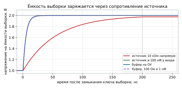
| What drives the ADC | After 200 ns | Error | In codes |
|---|---|---|---|
| 10 kΩ source directly | 1.973 V | −26.6 mV | 33 |
| source plus 100 nF at the input | 1.99995 V | −0.05 mV | 0.06 |
| op-amp buffer | 2.00001 V | +0.01 mV | 0 |
| buffer, 100 Ω and 1 nF | 1.99921 V | −0.79 mV | 1 |
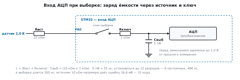
After 50 ns the difference is even clearer: straight from the source the capacitor holds 1.594 V instead of 2.0 — there is nothing to measure yet — while with the buffer it is already 2.000 V.
180.2 A capacitor at the input or a buffer
A 100 nF capacitor at the input works as a local charge reservoir: the sampling capacitor is 20000 times smaller, and recharging it pulls the capacitor down by only 0.05 mV. It is cheap and needs no amplifier — but it has a price:
- the capacitor together with a 10 kΩ source gives a 1 ms time constant: it will smooth a fast signal (sometimes that is exactly what you want — section 178);
- when the internal multiplexer switches channels, the capacitor actually helps: each pin has its own, and it supplies the charge to the sampling capacitor that the previous channel left charged. In the model, after a step from 3.0 to 0.5 V the error is 0.125 mV (5 pF · 2.5 V / 100 nF). It does not help behind an external multiplexer, where one ADC pin serves several sensors: there the capacitor is shared, and it has to be recharged as well (180.3);
- the capacitor only saves you with infrequent samples. Each sample takes
Cs · ΔUfrom it (ΔU is the difference from the previous channel), and it recharges through the source with the same 1 ms time constant. If samples come more often, the dips add up, and on average the input behaves like a resistor1 / (Cs · f): 200 kΩ at 5 pF and a million samples per second. With a 10 kΩ source that is a divider — an error of almost 5 % of the step, about 120 mV. The error stays below half a code (0.4 mV) up to roughly 2700 samples per second on the channel; - the leakage current of the capacitor and of the input adds to the error (section 164.1).
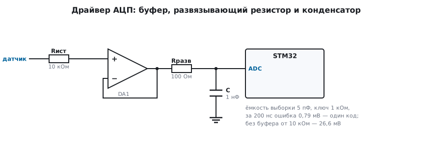
A buffer solves both problems: it keeps a low output impedance both for DC and for a fast signal. A typical ADC driver is a buffer, followed by a 100 Ω isolation resistor and a 1 nF capacitor right at the input: the resistor isolates the capacitance from the amplifier output (section 163.3), and the capacitor supplies the charge to the sampling capacitor. In the model this driver gives an error of 0.79 mV — one code.
180.3 Multiplexer: the neighbouring channel catches up
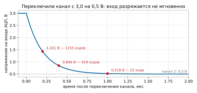
A microcontroller has one ADC for many channels: an internal multiplexer switches the input. What stays charged from the previous channel is the capacitance behind the multiplexer. For the internal one that is the sampling capacitor and the switch itself — a few picofarads, while the trace and protection at each pin are separate and charged by their own signal. If several sensors share one ADC pin through an external multiplexer, the common node also carries the trace, the protection and the capacitance of the multiplexer chip itself — 20 pF in the model. We switch such a multiplexer from a 3.0 V channel to a 0.5 V channel with 10 kΩ sources:
| Time after switching | Voltage at the ADC input | Error in codes |
|---|---|---|
| 200 ns | 1.431 V | 1155 |
| 400 ns | 0.846 V | 429 |
| 1 µs | 0.518 V | 22 |
| 2 µs | 0.500 V | 0.1 |
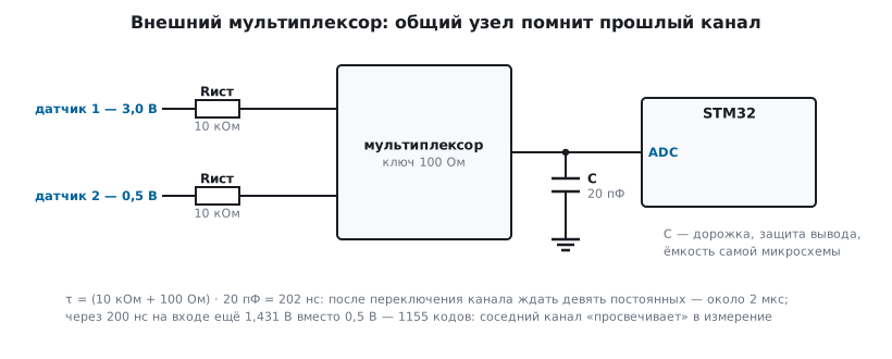
The time constant here is (10 kΩ + 100 Ω) · 20 pF = 202 ns, and after
switching you have to wait the same nine time constants. If you
don't, the neighbouring channel "shows through" into the measurement — on a large step
that is hundreds of codes. There are three cures: increase the sampling time in
the ADC settings, lower the source impedance (a buffer), or measure
each channel twice and keep the second value.
180.4 Source impedance: what the documentation says
The microcontroller documentation has a "maximum source
impedance" table for each sampling time. Its meaning is the same
as in 180.1, only the margin is stricter: the documentation uses ln 2^(N+2) — for
12 bits that is 9.7 time constants (settling to a quarter of a code), not 9:
9.7 · (Rsrc + Rsw) · Cs must fit into the sampling time. The practical conclusions:
- a sensor with a divider in the megohms cannot be measured directly at any sampling time: you need a buffer or a capacitor at the input with infrequent samples (180.2) — this is how section 166.5 measures a 1 MΩ / 1 MΩ battery divider;
- a thermistor in a 10 kΩ divider is borderline: it needs the longest sampling time;
- if there are many channels and they differ, the sampling time is set by the worst channel, or it is switched in software before each measurement.
180.5 At the DAC output — the same thing in reverse
The DAC also has resistors inside. The STM32 DAC has its own output buffer (section 15.3): with it the output drives loads from 5 kΩ, but does not reach the rails by about 0.2 V; without it the output impedance is up to 15 kΩ, and for 1 % accuracy the load must be 1.5 MΩ or more. An external buffer is added for a heavier load or for a signal that starts right at ground, and after it, if the signal is stepped, comes a reconstruction filter (section 178) that smooths the steps up to the update rate. PWM with an RC from section 50.5 is the same trick in a cheaper form.
180.6 Pitfalls
ADC readings are low and depend on the previous channel. Not enough sampling time: in the model with an external multiplexer, 200 ns after switching the input is at 1.431 V instead of 0.5.
A high-impedance sensor gives low codes. The source impedance is higher than allowed for the chosen sampling time — use a buffer.
After adding a 100 nF capacitor the signal became "blunt". The time constant with a 10 kΩ source is 1 ms; a fast signal needs a buffer.
The op-amp driver oscillates with the capacitance at the input. The isolation resistor is missing (section 163.3).
The DAC is wrong under load. The DAC output has its own impedance — it needs a buffer.
180.7 Summary
- The sampling time constant
(Rsrc + Rsw) · Cs= 55 ns; for 12 bits you need nine time constants — 496 ns, while sampling lasts 200 ns. - A 10 kΩ source directly gives an error of 26.6 mV (33 codes), a 100 nF capacitor at the input 0.05 mV, a buffer 0.01 mV, a driver with 100 Ω and 1 nF 0.79 mV.
- After a channel switch the common node behind an external multiplexer (20 pF) still holds the previous voltage: after 200 ns it is 1.431 V instead of 0.5 V — 1155 codes of error. With the internal multiplexer, a 100 nF capacitor at the pin brings this down to 0.125 mV.
- The "maximum source impedance" table in the documentation is exactly
the condition
9.7 · (Rsrc + Rsw) · Cs≤ sampling time.
Next: section 181 "Analog layout: common ground, interference, shielding".