 Embedded HandbookApps
181. Analog layout: common ground, interference, shielding
A circuit can be flawless and the measurement still bad: the noise arrives not through the input but through the ground and through the capacitance between traces. Section 130 covered the general rules of the circuit board; here we look at what exactly the analog path loses and what it costs in ADC codes.
The numbers below come from ngspice models: a 2.000 V signal from a sensor with 10 kΩ resistance, a 12-bit ADC with a 3.3 V full scale (one code is 0.806 mV).
Terms used in the documentation
Term Meaning ground bounce a jump in the ground potential common return path a return conductor shared by several circuits star ground / single-point ground grounds joined at one point analog / digital ground the ground of the analog part / of the digital part crosstalk, coupling capacitance noise picked up from a neighbour, the capacitance that couples it guard ring / guard trace a ring or trace around a node at the node's own potential loop area the area enclosed by a current and its return shield a conductive screen against interference
181.1 Common return path
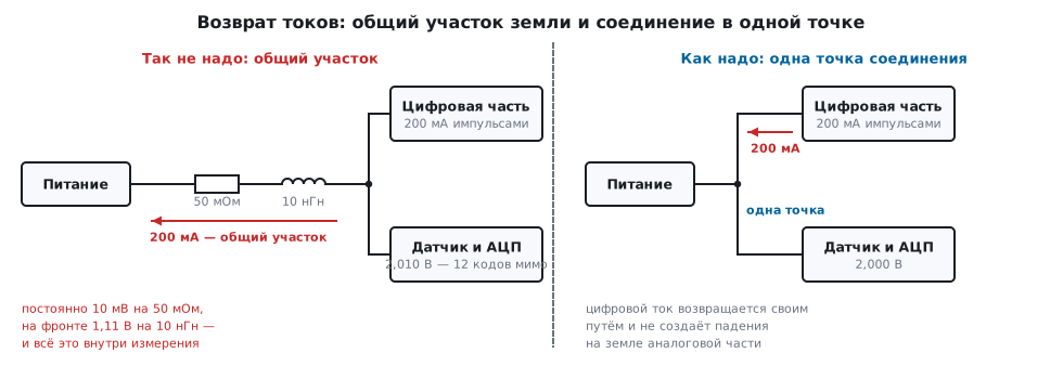
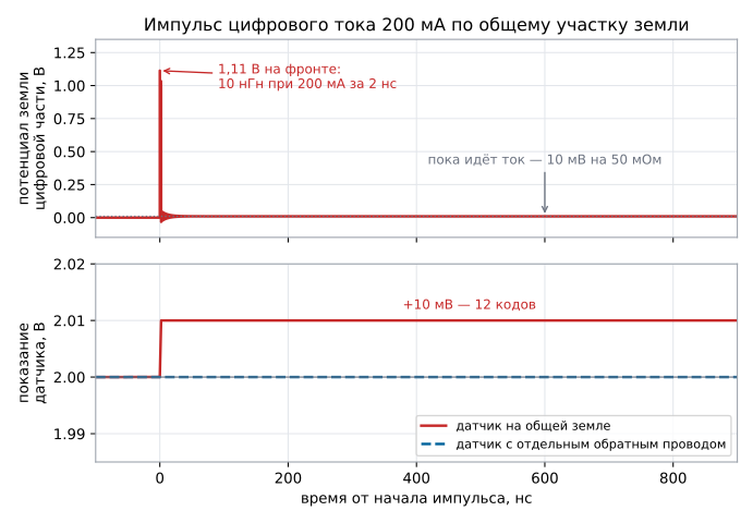
Suppose the digital part draws 200 mA pulses with a 2 ns edge, and its current returns to the supply over the same piece of ground that the sensor is referenced to. That piece is 50 mΩ and 10 nH:
| What we measure | Value |
|---|---|
| ground bounce on the current edge | 1.11 V |
| sensor reading on the common ground | 2.010 V — error 10 mV, 12 codes |
| sensor reading with a separate return conductor | 2.000 V |
The steady part of the error is Ohm's law: 200 mA through 50 mΩ gives 10 mV, and all of it goes into the measurement. The pulsed part depends on the edge: 10 nH with 200 mA in 2 ns gives more than a volt — and every circuit that treats this very piece as "ground" sees that jump. Fast digital outputs have such edges; a switch for an LED or a relay has edges of hundreds of nanoseconds (172.3), and the same 10 nH add only a few millivolts.
The cure is not "a thicker trace" but separate paths: the return current of the digital part must not flow through a piece shared with the analog part. Where the ground is wires and traces, they are joined at one point — usually under the ADC ground pin or at the power connector; what to do with a solid ground plane is covered in 181.3.
181.2 Crosstalk through the capacitance between traces
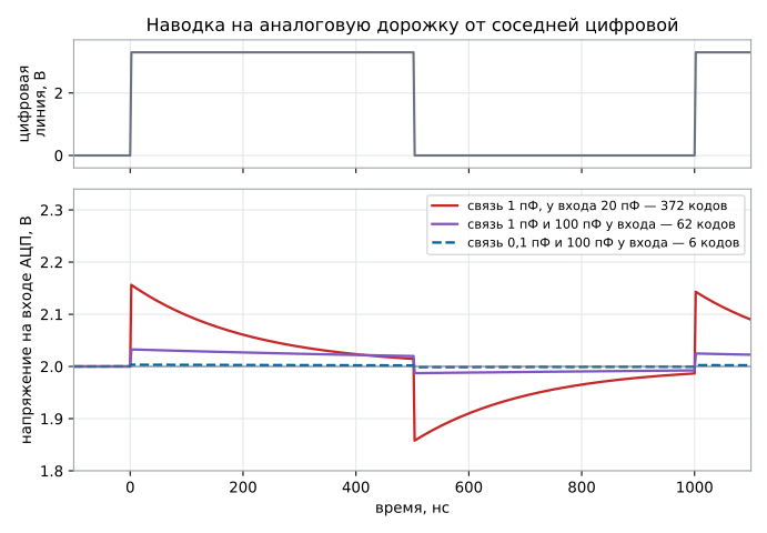
Two traces side by side form a capacitor. Suppose a digital line switches between 0 and 3.3 V with 2 ns edges, and next to it runs an analog trace from a sensor with 10 kΩ resistance:
| Coupling and input | Noise swing | In codes |
|---|---|---|
| 1 pF, only 20 pF of trace at the input | 1.857…2.156 V | 372 |
| 1 pF and a 100 pF capacitor at the input | 1.982…2.033 V | 62 |
| 0.1 pF and a 100 pF capacitor at the input | 1.998…2.003 V | 6 |
One picofarad is a centimetre of parallel traces on adjacent layers.
The noise comes not "with the level" but with the edge. In 2 ns the 10 kΩ source
cannot do anything — the time constant Rsrc · (Cc + Cin) = 10 kΩ · 21 pF
= 210 ns — and the step is simply divided by the capacitances: ΔU = U · Cc / (Cc + Cin) =
3.3 · 1 / 21 = 157 mV; in the model it is 2.156 V against 2.000 V without noise.
With a 100 pF capacitor at the input it is 3.3 · 1 / 101 = 33 mV. Then the noise drains away
through the source with the same time constant.
This gives three measures, in order of effectiveness:
- move the traces apart — reduce the coupling capacitance (in the model from 1 to 0.1 pF, the error drops from 372 to 6 codes);
- a ground trace or plane between them — it takes the coupled noise onto itself;
- a capacitor at the ADC input (section 180.2) — it reduces the swing but does not remove the coupling: 62 codes instead of 372.
181.3 Rules that work
- One ground plane — and separation by placement. On a board with a solid ground plane there are no separate "analog" and "digital" grounds, and the plane is not cut: the analog part is placed so that the return currents of the digital part and the power circuits do not pass under it. A single-point connection is for separate wires and two-layer boards without a ground plane: there the digital and power returns are routed on their own traces to a point at the ADC ground pin or at the power connector.
- The return current flows under the trace. At frequencies above a few hundred kilohertz the return current flows in the ground plane right under the signal trace: do not break the plane under an analog circuit — the current will go around and form a loop.
- Keep the analog parts in a compact group: divider, filter, buffer and input capacitor close together, traces short.
- The reference and its capacitor go at the pin (section 177), supply decoupling at every supply pin (section 167.5).
- Surround high-impedance nodes with a guard ring — a trace at the same potential as the input: it intercepts leakage currents across the board surface (the same ones that stop a watch crystal in 174.5).
- Do not run an analog trace next to a clock, PWM or interface line. If a crossing is unavoidable, cross at a right angle.
181.4 What to check before the board is made
- Where the return current of each high-current circuit physically flows, and whether it crosses the analog ground.
- Whether there is a solid ground plane under the analog part and whether it is cut.
- The length and neighbours of the analog traces: what runs next to them and with what edges.
- Decoupling capacitors — at the pins, not "wherever they fit".
- The capacitor at the ADC input and the isolation resistor (section 180.2).
- The reference, its capacitor and the path of its ground.
181.5 Pitfalls
Readings jump when a relay or a backlight switches on. A common return path: 200 mA through 50 mΩ is 10 mV, 12 codes.
The clock or PWM frequency shows up in the readings. Crosstalk through the capacitance of neighbouring traces.
A capacitor was added at the input, but the noise stayed. It reduces the swing but does not remove the coupling: 62 codes instead of 372.
The ground plane was cut "to separate the analog part" — and it got worse. The return current went around, and the loop area grew.
A high-impedance sensor "drifts" in humid air. Leakage currents across the board surface — you need a guard ring and cleaning.
181.6 Summary
- A shared 50 mΩ piece of ground at 200 mA gives 10 mV of error — 12 codes, and on the edge 10 nH kick the ground up by 1.11 V.
- A coupling capacitance of 1 pF between a digital and an analog trace gives a noise swing of 372 codes; a 100 pF capacitor at the input leaves 62, moving the traces apart to 0.1 pF leaves 6.
- Ground wires are joined at one point; a solid ground plane is not cut, and digital and power currents are kept away from the analog part by placement; high-impedance nodes are surrounded with a guard ring.
Next: section 182 "Firmware lifecycle and the cost of a defect".