 Embedded HandbookПриложения
Приложение A13. Карты регистров STM32L1
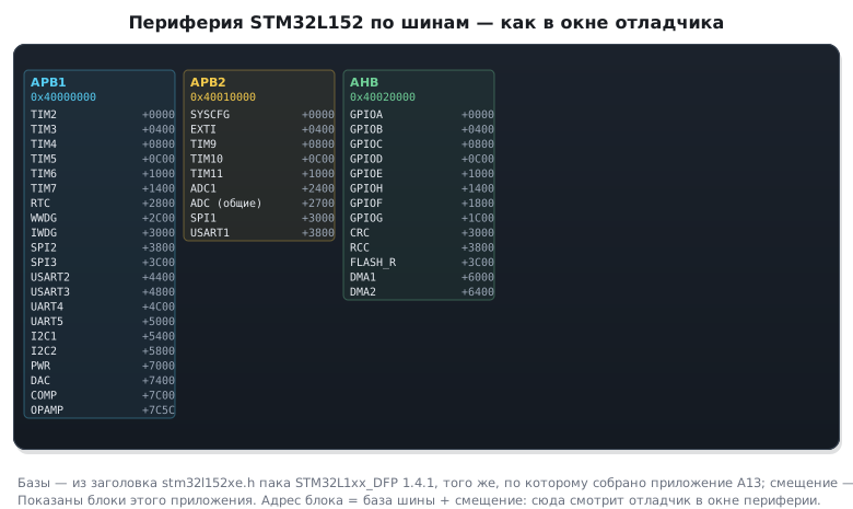
Серия STM32L1: Cortex-M3 до 32 МГц — первая малопотребляющая серия, контроллер ЖКИ. Регистры и биты основных блоков — из заголовка STM32L152, тем же генератором, что карты F1 и F4: смещения — по структурам *_TypeDef, назначение регистра и описание бита — из комментариев заголовка. Блоки, которых в серии нет, опущены. Для малого потребления смотрите PWR (режимы сна), RCC (генераторы LSE/LSI/MSI), LPTIM и LPUART — они работают во сне. Разделы справочника написаны для F103 и F407; имена регистров и битов у серий в основном те же — карта помогает перенести код и увидеть, что устроено иначе.
Как читать: смещение — от базового адреса блока; 31:16 — поле битов
с 16 по 31; одно число — отдельный бит. Цифра в скобках у заголовка
блока — раздел, где блок разобран.
RCC — Тактирование (раздел 6)
| Регистр | Смещение | Бит | Назначение |
|---|---|---|---|
CR |
0x00 |
32 | RCC clock control register |
RCC_CR_HSION |
0 | Internal High Speed clock enable | |
RCC_CR_HSIRDY |
1 | Internal High Speed clock ready flag | |
RCC_CR_MSION |
8 | Internal Multi Speed clock enable | |
RCC_CR_MSIRDY |
9 | Internal Multi Speed clock ready flag | |
RCC_CR_HSEON |
16 | External High Speed clock enable | |
RCC_CR_HSERDY |
17 | External High Speed clock ready flag | |
RCC_CR_HSEBYP |
18 | External High Speed clock Bypass | |
RCC_CR_PLLON |
24 | PLL enable | |
RCC_CR_PLLRDY |
25 | PLL clock ready flag | |
RCC_CR_CSSON |
28 | Clock Security System enable | |
RCC_CR_RTCPRE |
29:30 | RTC/LCD Prescaler | |
ICSCR |
0x04 |
32 | RCC Internal clock sources calibration register |
RCC_ICSCR_HSICAL |
0:7 | Internal High Speed clock Calibration | |
RCC_ICSCR_HSITRIM |
8:12 | Internal High Speed clock trimming | |
RCC_ICSCR_MSIRANGE |
13:15 | Internal Multi Speed clock Range | |
RCC_ICSCR_MSICAL |
16:23 | Internal Multi Speed clock Calibration | |
RCC_ICSCR_MSITRIM |
24:31 | Internal Multi Speed clock trimming | |
CFGR |
0x08 |
32 | RCC Clock configuration register |
RCC_CFGR_SW |
0:1 | SW[1:0] bits (System clock Switch) | |
RCC_CFGR_SWS |
2:3 | SWS[1:0] bits (System Clock Switch Status) | |
RCC_CFGR_HPRE |
4:7 | HPRE[3:0] bits (AHB prescaler) | |
RCC_CFGR_PPRE1 |
8:10 | PRE1[2:0] bits (APB1 prescaler) | |
RCC_CFGR_PPRE2 |
11:13 | PRE2[2:0] bits (APB2 prescaler) | |
RCC_CFGR_PLLSRC |
16 | PLL entry clock source | |
RCC_CFGR_PLLMUL |
18:21 | PLLMUL[3:0] bits (PLL multiplication factor) | |
RCC_CFGR_PLLDIV |
22:23 | PLLDIV[1:0] bits (PLL Output Division) | |
RCC_CFGR_PLLDIV2 |
22 | PLL clock output = CKVCO / 2 | |
RCC_CFGR_PLLDIV4 |
22:23 | PLL clock output = CKVCO / 4 | |
RCC_CFGR_PLLDIV3 |
23 | PLL clock output = CKVCO / 3 | |
RCC_CFGR_MCOSEL |
24:26 | MCO[2:0] bits (Microcontroller Clock Output) | |
RCC_CFGR_MCOSEL_SYSCLK |
24 | System clock selected | |
RCC_CFGR_MCOSEL_MSI |
24:25 | Internal Medium Speed RC oscillator clock selected | |
RCC_CFGR_MCOSEL_PLL |
24:26 | PLL clock divided | |
RCC_CFGR_MCOSEL_LSE |
24:26 | LSE selected | |
RCC_CFGR_MCOSEL_HSI |
25 | Internal 16 MHz RC oscillator clock selected | |
RCC_CFGR_MCOSEL_LSI |
25:26 | LSI selected | |
RCC_CFGR_MCOSEL_HSE |
26 | External 1-25 MHz oscillator clock selected | |
RCC_CFGR_MCOPRE |
28:30 | MCOPRE[2:0] bits (Microcontroller Clock Output Prescaler) | |
CIR |
0x0C |
32 | RCC Clock interrupt register |
RCC_CIR_LSIRDYF |
0 | LSI Ready Interrupt flag | |
RCC_CIR_LSERDYF |
1 | LSE Ready Interrupt flag | |
RCC_CIR_HSIRDYF |
2 | HSI Ready Interrupt flag | |
RCC_CIR_HSERDYF |
3 | HSE Ready Interrupt flag | |
RCC_CIR_PLLRDYF |
4 | PLL Ready Interrupt flag | |
RCC_CIR_MSIRDYF |
5 | MSI Ready Interrupt flag | |
RCC_CIR_LSECSSF |
6 | LSE CSS Interrupt flag | |
RCC_CIR_CSSF |
7 | Clock Security System Interrupt flag | |
RCC_CIR_LSIRDYIE |
8 | LSI Ready Interrupt Enable | |
RCC_CIR_LSERDYIE |
9 | LSE Ready Interrupt Enable | |
RCC_CIR_HSIRDYIE |
10 | HSI Ready Interrupt Enable | |
RCC_CIR_HSERDYIE |
11 | HSE Ready Interrupt Enable | |
RCC_CIR_PLLRDYIE |
12 | PLL Ready Interrupt Enable | |
RCC_CIR_MSIRDYIE |
13 | MSI Ready Interrupt Enable | |
RCC_CIR_LSECSSIE |
14 | LSE CSS Interrupt Enable | |
RCC_CIR_LSIRDYC |
16 | LSI Ready Interrupt Clear | |
RCC_CIR_LSERDYC |
17 | LSE Ready Interrupt Clear | |
RCC_CIR_HSIRDYC |
18 | HSI Ready Interrupt Clear | |
RCC_CIR_HSERDYC |
19 | HSE Ready Interrupt Clear | |
RCC_CIR_PLLRDYC |
20 | PLL Ready Interrupt Clear | |
RCC_CIR_MSIRDYC |
21 | MSI Ready Interrupt Clear | |
RCC_CIR_LSECSSC |
22 | LSE CSS Interrupt Clear | |
RCC_CIR_CSSC |
23 | Clock Security System Interrupt Clear | |
AHBRSTR |
0x10 |
32 | RCC AHB peripheral reset register |
RCC_AHBRSTR_GPIOARST |
0 | GPIO port A reset | |
RCC_AHBRSTR_GPIOBRST |
1 | GPIO port B reset | |
RCC_AHBRSTR_GPIOCRST |
2 | GPIO port C reset | |
RCC_AHBRSTR_GPIODRST |
3 | GPIO port D reset | |
RCC_AHBRSTR_GPIOERST |
4 | GPIO port E reset | |
RCC_AHBRSTR_GPIOHRST |
5 | GPIO port H reset | |
RCC_AHBRSTR_GPIOFRST |
6 | GPIO port F reset | |
RCC_AHBRSTR_GPIOGRST |
7 | GPIO port G reset | |
RCC_AHBRSTR_CRCRST |
12 | CRC reset | |
RCC_AHBRSTR_FLITFRST |
15 | FLITF reset | |
RCC_AHBRSTR_DMA1RST |
24 | DMA1 reset | |
RCC_AHBRSTR_DMA2RST |
25 | DMA2 reset | |
APB2RSTR |
0x14 |
32 | RCC APB2 peripheral reset register |
RCC_APB2RSTR_SYSCFGRST |
0 | System Configuration SYSCFG reset | |
RCC_APB2RSTR_TIM9RST |
2 | TIM9 reset | |
RCC_APB2RSTR_TIM10RST |
3 | TIM10 reset | |
RCC_APB2RSTR_TIM11RST |
4 | TIM11 reset | |
RCC_APB2RSTR_ADC1RST |
9 | ADC1 reset | |
RCC_APB2RSTR_SPI1RST |
12 | SPI1 reset | |
RCC_APB2RSTR_USART1RST |
14 | USART1 reset | |
APB1RSTR |
0x18 |
32 | RCC APB1 peripheral reset register |
RCC_APB1RSTR_TIM2RST |
0 | Timer 2 reset | |
RCC_APB1RSTR_TIM3RST |
1 | Timer 3 reset | |
RCC_APB1RSTR_TIM4RST |
2 | Timer 4 reset | |
RCC_APB1RSTR_TIM5RST |
3 | Timer 5 reset | |
RCC_APB1RSTR_TIM6RST |
4 | Timer 6 reset | |
RCC_APB1RSTR_TIM7RST |
5 | Timer 7 reset | |
RCC_APB1RSTR_LCDRST |
9 | LCD reset | |
RCC_APB1RSTR_WWDGRST |
11 | Window Watchdog reset | |
RCC_APB1RSTR_SPI2RST |
14 | SPI 2 reset | |
RCC_APB1RSTR_SPI3RST |
15 | SPI 3 reset | |
RCC_APB1RSTR_USART2RST |
17 | USART 2 reset | |
RCC_APB1RSTR_USART3RST |
18 | USART 3 reset | |
RCC_APB1RSTR_UART4RST |
19 | UART 4 reset | |
RCC_APB1RSTR_UART5RST |
20 | UART 5 reset | |
RCC_APB1RSTR_I2C1RST |
21 | I2C 1 reset | |
RCC_APB1RSTR_I2C2RST |
22 | I2C 2 reset | |
RCC_APB1RSTR_USBRST |
23 | USB reset | |
RCC_APB1RSTR_PWRRST |
28 | Power interface reset | |
RCC_APB1RSTR_DACRST |
29 | DAC interface reset | |
RCC_APB1RSTR_COMPRST |
31 | Comparator interface reset | |
AHBENR |
0x1C |
32 | RCC AHB peripheral clock enable register |
RCC_AHBENR_GPIOAEN |
0 | GPIO port A clock enable | |
RCC_AHBENR_GPIOBEN |
1 | GPIO port B clock enable | |
RCC_AHBENR_GPIOCEN |
2 | GPIO port C clock enable | |
RCC_AHBENR_GPIODEN |
3 | GPIO port D clock enable | |
RCC_AHBENR_GPIOEEN |
4 | GPIO port E clock enable | |
RCC_AHBENR_GPIOHEN |
5 | GPIO port H clock enable | |
RCC_AHBENR_GPIOFEN |
6 | GPIO port F clock enable | |
RCC_AHBENR_GPIOGEN |
7 | GPIO port G clock enable | |
RCC_AHBENR_CRCEN |
12 | CRC clock enable | |
RCC_AHBENR_FLITFEN |
15 | ||
RCC_AHBENR_DMA1EN |
24 | DMA1 clock enable | |
RCC_AHBENR_DMA2EN |
25 | DMA2 clock enable | |
APB2ENR |
0x20 |
32 | RCC APB2 peripheral clock enable register |
RCC_APB2ENR_SYSCFGEN |
0 | System Configuration SYSCFG clock enable | |
RCC_APB2ENR_TIM9EN |
2 | TIM9 interface clock enable | |
RCC_APB2ENR_TIM10EN |
3 | TIM10 interface clock enable | |
RCC_APB2ENR_TIM11EN |
4 | TIM11 Timer clock enable | |
RCC_APB2ENR_ADC1EN |
9 | ADC1 clock enable | |
RCC_APB2ENR_SPI1EN |
12 | SPI1 clock enable | |
RCC_APB2ENR_USART1EN |
14 | USART1 clock enable | |
APB1ENR |
0x24 |
32 | RCC APB1 peripheral clock enable register |
RCC_APB1ENR_TIM2EN |
0 | Timer 2 clock enabled | |
RCC_APB1ENR_TIM3EN |
1 | Timer 3 clock enable | |
RCC_APB1ENR_TIM4EN |
2 | Timer 4 clock enable | |
RCC_APB1ENR_TIM5EN |
3 | Timer 5 clock enable | |
RCC_APB1ENR_TIM6EN |
4 | Timer 6 clock enable | |
RCC_APB1ENR_TIM7EN |
5 | Timer 7 clock enable | |
RCC_APB1ENR_LCDEN |
9 | LCD clock enable | |
RCC_APB1ENR_WWDGEN |
11 | Window Watchdog clock enable | |
RCC_APB1ENR_SPI2EN |
14 | SPI 2 clock enable | |
RCC_APB1ENR_SPI3EN |
15 | SPI 3 clock enable | |
RCC_APB1ENR_USART2EN |
17 | USART 2 clock enable | |
RCC_APB1ENR_USART3EN |
18 | USART 3 clock enable | |
RCC_APB1ENR_UART4EN |
19 | UART 4 clock enable | |
RCC_APB1ENR_UART5EN |
20 | UART 5 clock enable | |
RCC_APB1ENR_I2C1EN |
21 | I2C 1 clock enable | |
RCC_APB1ENR_I2C2EN |
22 | I2C 2 clock enable | |
RCC_APB1ENR_USBEN |
23 | USB clock enable | |
RCC_APB1ENR_PWREN |
28 | Power interface clock enable | |
RCC_APB1ENR_DACEN |
29 | DAC interface clock enable | |
RCC_APB1ENR_COMPEN |
31 | Comparator interface clock enable | |
AHBLPENR |
0x28 |
32 | RCC AHB peripheral clock enable in low power mode register |
RCC_AHBLPENR_GPIOALPEN |
0 | GPIO port A clock enabled in sleep mode | |
RCC_AHBLPENR_GPIOBLPEN |
1 | GPIO port B clock enabled in sleep mode | |
RCC_AHBLPENR_GPIOCLPEN |
2 | GPIO port C clock enabled in sleep mode | |
RCC_AHBLPENR_GPIODLPEN |
3 | GPIO port D clock enabled in sleep mode | |
RCC_AHBLPENR_GPIOELPEN |
4 | GPIO port E clock enabled in sleep mode | |
RCC_AHBLPENR_GPIOHLPEN |
5 | GPIO port H clock enabled in sleep mode | |
RCC_AHBLPENR_GPIOFLPEN |
6 | GPIO port F clock enabled in sleep mode | |
RCC_AHBLPENR_GPIOGLPEN |
7 | GPIO port G clock enabled in sleep mode | |
RCC_AHBLPENR_CRCLPEN |
12 | CRC clock enabled in sleep mode | |
RCC_AHBLPENR_FLITFLPEN |
15 | ||
RCC_AHBLPENR_SRAMLPEN |
16 | SRAM clock enabled in sleep mode | |
RCC_AHBLPENR_DMA1LPEN |
24 | DMA1 clock enabled in sleep mode | |
RCC_AHBLPENR_DMA2LPEN |
25 | DMA2 clock enabled in sleep mode | |
APB2LPENR |
0x2C |
32 | RCC APB2 peripheral clock enable in low power mode register |
RCC_APB2LPENR_SYSCFGLPEN |
0 | System Configuration SYSCFG clock enabled in sleep mode | |
RCC_APB2LPENR_TIM9LPEN |
2 | TIM9 interface clock enabled in sleep mode | |
RCC_APB2LPENR_TIM10LPEN |
3 | TIM10 interface clock enabled in sleep mode | |
RCC_APB2LPENR_TIM11LPEN |
4 | TIM11 Timer clock enabled in sleep mode | |
RCC_APB2LPENR_ADC1LPEN |
9 | ADC1 clock enabled in sleep mode | |
RCC_APB2LPENR_SPI1LPEN |
12 | SPI1 clock enabled in sleep mode | |
RCC_APB2LPENR_USART1LPEN |
14 | USART1 clock enabled in sleep mode | |
APB1LPENR |
0x30 |
32 | RCC APB1 peripheral clock enable in low power mode register |
RCC_APB1LPENR_TIM2LPEN |
0 | Timer 2 clock enabled in sleep mode | |
RCC_APB1LPENR_TIM3LPEN |
1 | Timer 3 clock enabled in sleep mode | |
RCC_APB1LPENR_TIM4LPEN |
2 | Timer 4 clock enabled in sleep mode | |
RCC_APB1LPENR_TIM5LPEN |
3 | Timer 5 clock enabled in sleep mode | |
RCC_APB1LPENR_TIM6LPEN |
4 | Timer 6 clock enabled in sleep mode | |
RCC_APB1LPENR_TIM7LPEN |
5 | Timer 7 clock enabled in sleep mode | |
RCC_APB1LPENR_LCDLPEN |
9 | LCD clock enabled in sleep mode | |
RCC_APB1LPENR_WWDGLPEN |
11 | Window Watchdog clock enabled in sleep mode | |
RCC_APB1LPENR_SPI2LPEN |
14 | SPI 2 clock enabled in sleep mode | |
RCC_APB1LPENR_SPI3LPEN |
15 | SPI 3 clock enabled in sleep mode | |
RCC_APB1LPENR_USART2LPEN |
17 | USART 2 clock enabled in sleep mode | |
RCC_APB1LPENR_USART3LPEN |
18 | USART 3 clock enabled in sleep mode | |
RCC_APB1LPENR_UART4LPEN |
19 | UART 4 clock enabled in sleep mode | |
RCC_APB1LPENR_UART5LPEN |
20 | UART 5 clock enabled in sleep mode | |
RCC_APB1LPENR_I2C1LPEN |
21 | I2C 1 clock enabled in sleep mode | |
RCC_APB1LPENR_I2C2LPEN |
22 | I2C 2 clock enabled in sleep mode | |
RCC_APB1LPENR_USBLPEN |
23 | USB clock enabled in sleep mode | |
RCC_APB1LPENR_PWRLPEN |
28 | Power interface clock enabled in sleep mode | |
RCC_APB1LPENR_DACLPEN |
29 | DAC interface clock enabled in sleep mode | |
RCC_APB1LPENR_COMPLPEN |
31 | Comparator interface clock enabled in sleep mode | |
CSR |
0x34 |
32 | RCC Control/status register |
RCC_CSR_LSION |
0 | Internal Low Speed oscillator enable | |
RCC_CSR_LSIRDY |
1 | Internal Low Speed oscillator Ready | |
RCC_CSR_LSEON |
8 | External Low Speed oscillator enable | |
RCC_CSR_LSERDY |
9 | External Low Speed oscillator Ready | |
RCC_CSR_LSEBYP |
10 | External Low Speed oscillator Bypass | |
RCC_CSR_LSECSSON |
11 | External Low Speed oscillator CSS Enable | |
RCC_CSR_LSECSSD |
12 | External Low Speed oscillator CSS Detected | |
RCC_CSR_RTCSEL |
16:17 | RTCSEL[1:0] bits (RTC clock source selection) | |
RCC_CSR_RTCSEL_LSE |
16 | LSE oscillator clock used as RTC clock | |
RCC_CSR_RTCSEL_HSE |
16:17 | HSE oscillator clock divided by 2, 4, 8 or 16 by RTCPRE used as RTC clock | |
RCC_CSR_RTCSEL_LSI |
17 | LSI oscillator clock used as RTC clock | |
RCC_CSR_RTCEN |
22 | RTC clock enable | |
RCC_CSR_RTCRST |
23 | RTC reset | |
RCC_CSR_RMVF |
24 | Remove reset flag | |
RCC_CSR_OBLRSTF |
25 | Option Bytes Loader reset flag | |
RCC_CSR_PINRSTF |
26 | PIN reset flag | |
RCC_CSR_PORRSTF |
27 | POR/PDR reset flag | |
RCC_CSR_SFTRSTF |
28 | Software Reset flag | |
RCC_CSR_IWDGRSTF |
29 | Independent Watchdog reset flag | |
RCC_CSR_WWDGRSTF |
30 | Window watchdog reset flag | |
RCC_CSR_LPWRRSTF |
31 | Low-Power reset flag |
GPIO — Порты ввода-вывода (раздел 8)
| Регистр | Смещение | Бит | Назначение |
|---|---|---|---|
MODER |
0x00 |
32 | GPIO port mode register |
GPIO_MODER_MODER0 |
0:1 | ||
GPIO_MODER_MODER1 |
2:3 | ||
GPIO_MODER_MODER2 |
4:5 | ||
GPIO_MODER_MODER3 |
6:7 | ||
GPIO_MODER_MODER4 |
8:9 | ||
GPIO_MODER_MODER5 |
10:11 | ||
GPIO_MODER_MODER6 |
12:13 | ||
GPIO_MODER_MODER7 |
14:15 | ||
GPIO_MODER_MODER8 |
16:17 | ||
GPIO_MODER_MODER9 |
18:19 | ||
GPIO_MODER_MODER10 |
20:21 | ||
GPIO_MODER_MODER11 |
22:23 | ||
GPIO_MODER_MODER12 |
24:25 | ||
GPIO_MODER_MODER13 |
26:27 | ||
GPIO_MODER_MODER14 |
28:29 | ||
GPIO_MODER_MODER15 |
30:31 | ||
OTYPER |
0x04 |
32 | GPIO port output type register |
OSPEEDR |
0x08 |
32 | GPIO port output speed register |
PUPDR |
0x0C |
32 | GPIO port pull-up/pull-down register |
GPIO_PUPDR_PUPDR0 |
0:1 | ||
GPIO_PUPDR_PUPDR1 |
2:3 | ||
GPIO_PUPDR_PUPDR2 |
4:5 | ||
GPIO_PUPDR_PUPDR3 |
6:7 | ||
GPIO_PUPDR_PUPDR4 |
8:9 | ||
GPIO_PUPDR_PUPDR5 |
10:11 | ||
GPIO_PUPDR_PUPDR6 |
12:13 | ||
GPIO_PUPDR_PUPDR7 |
14:15 | ||
GPIO_PUPDR_PUPDR8 |
16:17 | ||
GPIO_PUPDR_PUPDR9 |
18:19 | ||
GPIO_PUPDR_PUPDR10 |
20:21 | ||
GPIO_PUPDR_PUPDR11 |
22:23 | ||
GPIO_PUPDR_PUPDR12 |
24:25 | ||
GPIO_PUPDR_PUPDR13 |
26:27 | ||
GPIO_PUPDR_PUPDR14 |
28:29 | ||
GPIO_PUPDR_PUPDR15 |
30:31 | ||
IDR |
0x10 |
32 | GPIO port input data register |
ODR |
0x14 |
32 | GPIO port output data register |
BSRR |
0x18 |
32 | GPIO port bit set/reset registerBSRR |
LCKR |
0x1C |
32 | GPIO port configuration lock register |
GPIO_LCKR_LCK0 |
0 | ||
GPIO_LCKR_LCK1 |
1 | ||
GPIO_LCKR_LCK2 |
2 | ||
GPIO_LCKR_LCK3 |
3 | ||
GPIO_LCKR_LCK4 |
4 | ||
GPIO_LCKR_LCK5 |
5 | ||
GPIO_LCKR_LCK6 |
6 | ||
GPIO_LCKR_LCK7 |
7 | ||
GPIO_LCKR_LCK8 |
8 | ||
GPIO_LCKR_LCK9 |
9 | ||
GPIO_LCKR_LCK10 |
10 | ||
GPIO_LCKR_LCK11 |
11 | ||
GPIO_LCKR_LCK12 |
12 | ||
GPIO_LCKR_LCK13 |
13 | ||
GPIO_LCKR_LCK14 |
14 | ||
GPIO_LCKR_LCK15 |
15 | ||
GPIO_LCKR_LCKK |
16 | ||
AFR+2×4 |
0x20 |
32 | GPIO alternate function register |
BRR |
0x28 |
32 | GPIO bit reset register |
SYSCFG — Системная конфигурация (раздел 8)
| Регистр | Смещение | Бит | Назначение |
|---|---|---|---|
MEMRMP |
0x00 |
32 | SYSCFG memory remap register |
SYSCFG_MEMRMP_MEM_MODE |
0:1 | SYSCFG_Memory Remap Config | |
SYSCFG_MEMRMP_BOOT_MODE |
8:9 | Boot mode Config | |
PMC |
0x04 |
32 | SYSCFG peripheral mode configuration register |
SYSCFG_PMC_USB_PU |
0 | SYSCFG PMC | |
SYSCFG_PMC_LCD_CAPA |
1:5 | LCD_CAPA decoupling capacitance connection | |
EXTICR+4×4 |
0x08 |
32 | SYSCFG external interrupt configuration registers |
EXTI — Внешние прерывания (раздел 7)
| Регистр | Смещение | Бит | Назначение |
|---|---|---|---|
IMR |
0x00 |
32 | EXTI Interrupt mask register |
EXTI_IMR_MR0 |
0 | Interrupt Mask on line 0 | |
EXTI_IMR_IM |
0:23 | Interrupt Mask All | |
EXTI_IMR_MR1 |
1 | Interrupt Mask on line 1 | |
EXTI_IMR_MR2 |
2 | Interrupt Mask on line 2 | |
EXTI_IMR_MR3 |
3 | Interrupt Mask on line 3 | |
EXTI_IMR_MR4 |
4 | Interrupt Mask on line 4 | |
EXTI_IMR_MR5 |
5 | Interrupt Mask on line 5 | |
EXTI_IMR_MR6 |
6 | Interrupt Mask on line 6 | |
EXTI_IMR_MR7 |
7 | Interrupt Mask on line 7 | |
EXTI_IMR_MR8 |
8 | Interrupt Mask on line 8 | |
EXTI_IMR_MR9 |
9 | Interrupt Mask on line 9 | |
EXTI_IMR_MR10 |
10 | Interrupt Mask on line 10 | |
EXTI_IMR_MR11 |
11 | Interrupt Mask on line 11 | |
EXTI_IMR_MR12 |
12 | Interrupt Mask on line 12 | |
EXTI_IMR_MR13 |
13 | Interrupt Mask on line 13 | |
EXTI_IMR_MR14 |
14 | Interrupt Mask on line 14 | |
EXTI_IMR_MR15 |
15 | Interrupt Mask on line 15 | |
EXTI_IMR_MR16 |
16 | Interrupt Mask on line 16 | |
EXTI_IMR_MR17 |
17 | Interrupt Mask on line 17 | |
EXTI_IMR_MR18 |
18 | Interrupt Mask on line 18 | |
EXTI_IMR_MR19 |
19 | Interrupt Mask on line 19 | |
EXTI_IMR_MR20 |
20 | Interrupt Mask on line 20 | |
EXTI_IMR_MR21 |
21 | Interrupt Mask on line 21 | |
EXTI_IMR_MR22 |
22 | Interrupt Mask on line 22 | |
EXTI_IMR_MR23 |
23 | Interrupt Mask on line 23 | |
EMR |
0x04 |
32 | EXTI Event mask register |
EXTI_EMR_MR0 |
0 | Event Mask on line 0 | |
EXTI_EMR_MR1 |
1 | Event Mask on line 1 | |
EXTI_EMR_MR2 |
2 | Event Mask on line 2 | |
EXTI_EMR_MR3 |
3 | Event Mask on line 3 | |
EXTI_EMR_MR4 |
4 | Event Mask on line 4 | |
EXTI_EMR_MR5 |
5 | Event Mask on line 5 | |
EXTI_EMR_MR6 |
6 | Event Mask on line 6 | |
EXTI_EMR_MR7 |
7 | Event Mask on line 7 | |
EXTI_EMR_MR8 |
8 | Event Mask on line 8 | |
EXTI_EMR_MR9 |
9 | Event Mask on line 9 | |
EXTI_EMR_MR10 |
10 | Event Mask on line 10 | |
EXTI_EMR_MR11 |
11 | Event Mask on line 11 | |
EXTI_EMR_MR12 |
12 | Event Mask on line 12 | |
EXTI_EMR_MR13 |
13 | Event Mask on line 13 | |
EXTI_EMR_MR14 |
14 | Event Mask on line 14 | |
EXTI_EMR_MR15 |
15 | Event Mask on line 15 | |
EXTI_EMR_MR16 |
16 | Event Mask on line 16 | |
EXTI_EMR_MR17 |
17 | Event Mask on line 17 | |
EXTI_EMR_MR18 |
18 | Event Mask on line 18 | |
EXTI_EMR_MR19 |
19 | Event Mask on line 19 | |
EXTI_EMR_MR20 |
20 | Event Mask on line 20 | |
EXTI_EMR_MR21 |
21 | Event Mask on line 21 | |
EXTI_EMR_MR22 |
22 | Event Mask on line 22 | |
EXTI_EMR_MR23 |
23 | Event Mask on line 23 | |
RTSR |
0x08 |
32 | EXTI Rising trigger selection register |
EXTI_RTSR_TR0 |
0 | Rising trigger event configuration bit of line 0 | |
EXTI_RTSR_TR1 |
1 | Rising trigger event configuration bit of line 1 | |
EXTI_RTSR_TR2 |
2 | Rising trigger event configuration bit of line 2 | |
EXTI_RTSR_TR3 |
3 | Rising trigger event configuration bit of line 3 | |
EXTI_RTSR_TR4 |
4 | Rising trigger event configuration bit of line 4 | |
EXTI_RTSR_TR5 |
5 | Rising trigger event configuration bit of line 5 | |
EXTI_RTSR_TR6 |
6 | Rising trigger event configuration bit of line 6 | |
EXTI_RTSR_TR7 |
7 | Rising trigger event configuration bit of line 7 | |
EXTI_RTSR_TR8 |
8 | Rising trigger event configuration bit of line 8 | |
EXTI_RTSR_TR9 |
9 | Rising trigger event configuration bit of line 9 | |
EXTI_RTSR_TR10 |
10 | Rising trigger event configuration bit of line 10 | |
EXTI_RTSR_TR11 |
11 | Rising trigger event configuration bit of line 11 | |
EXTI_RTSR_TR12 |
12 | Rising trigger event configuration bit of line 12 | |
EXTI_RTSR_TR13 |
13 | Rising trigger event configuration bit of line 13 | |
EXTI_RTSR_TR14 |
14 | Rising trigger event configuration bit of line 14 | |
EXTI_RTSR_TR15 |
15 | Rising trigger event configuration bit of line 15 | |
EXTI_RTSR_TR16 |
16 | Rising trigger event configuration bit of line 16 | |
EXTI_RTSR_TR17 |
17 | Rising trigger event configuration bit of line 17 | |
EXTI_RTSR_TR18 |
18 | Rising trigger event configuration bit of line 18 | |
EXTI_RTSR_TR19 |
19 | Rising trigger event configuration bit of line 19 | |
EXTI_RTSR_TR20 |
20 | Rising trigger event configuration bit of line 20 | |
EXTI_RTSR_TR21 |
21 | Rising trigger event configuration bit of line 21 | |
EXTI_RTSR_TR22 |
22 | Rising trigger event configuration bit of line 22 | |
EXTI_RTSR_TR23 |
23 | Rising trigger event configuration bit of line 23 | |
FTSR |
0x0C |
32 | EXTI Falling trigger selection register |
EXTI_FTSR_TR0 |
0 | Falling trigger event configuration bit of line 0 | |
EXTI_FTSR_TR1 |
1 | Falling trigger event configuration bit of line 1 | |
EXTI_FTSR_TR2 |
2 | Falling trigger event configuration bit of line 2 | |
EXTI_FTSR_TR3 |
3 | Falling trigger event configuration bit of line 3 | |
EXTI_FTSR_TR4 |
4 | Falling trigger event configuration bit of line 4 | |
EXTI_FTSR_TR5 |
5 | Falling trigger event configuration bit of line 5 | |
EXTI_FTSR_TR6 |
6 | Falling trigger event configuration bit of line 6 | |
EXTI_FTSR_TR7 |
7 | Falling trigger event configuration bit of line 7 | |
EXTI_FTSR_TR8 |
8 | Falling trigger event configuration bit of line 8 | |
EXTI_FTSR_TR9 |
9 | Falling trigger event configuration bit of line 9 | |
EXTI_FTSR_TR10 |
10 | Falling trigger event configuration bit of line 10 | |
EXTI_FTSR_TR11 |
11 | Falling trigger event configuration bit of line 11 | |
EXTI_FTSR_TR12 |
12 | Falling trigger event configuration bit of line 12 | |
EXTI_FTSR_TR13 |
13 | Falling trigger event configuration bit of line 13 | |
EXTI_FTSR_TR14 |
14 | Falling trigger event configuration bit of line 14 | |
EXTI_FTSR_TR15 |
15 | Falling trigger event configuration bit of line 15 | |
EXTI_FTSR_TR16 |
16 | Falling trigger event configuration bit of line 16 | |
EXTI_FTSR_TR17 |
17 | Falling trigger event configuration bit of line 17 | |
EXTI_FTSR_TR18 |
18 | Falling trigger event configuration bit of line 18 | |
EXTI_FTSR_TR19 |
19 | Falling trigger event configuration bit of line 19 | |
EXTI_FTSR_TR20 |
20 | Falling trigger event configuration bit of line 20 | |
EXTI_FTSR_TR21 |
21 | Falling trigger event configuration bit of line 21 | |
EXTI_FTSR_TR22 |
22 | Falling trigger event configuration bit of line 22 | |
EXTI_FTSR_TR23 |
23 | Falling trigger event configuration bit of line 23 | |
SWIER |
0x10 |
32 | EXTI Software interrupt event register |
EXTI_SWIER_SWIER0 |
0 | Software Interrupt on line 0 | |
EXTI_SWIER_SWIER1 |
1 | Software Interrupt on line 1 | |
EXTI_SWIER_SWIER2 |
2 | Software Interrupt on line 2 | |
EXTI_SWIER_SWIER3 |
3 | Software Interrupt on line 3 | |
EXTI_SWIER_SWIER4 |
4 | Software Interrupt on line 4 | |
EXTI_SWIER_SWIER5 |
5 | Software Interrupt on line 5 | |
EXTI_SWIER_SWIER6 |
6 | Software Interrupt on line 6 | |
EXTI_SWIER_SWIER7 |
7 | Software Interrupt on line 7 | |
EXTI_SWIER_SWIER8 |
8 | Software Interrupt on line 8 | |
EXTI_SWIER_SWIER9 |
9 | Software Interrupt on line 9 | |
EXTI_SWIER_SWIER10 |
10 | Software Interrupt on line 10 | |
EXTI_SWIER_SWIER11 |
11 | Software Interrupt on line 11 | |
EXTI_SWIER_SWIER12 |
12 | Software Interrupt on line 12 | |
EXTI_SWIER_SWIER13 |
13 | Software Interrupt on line 13 | |
EXTI_SWIER_SWIER14 |
14 | Software Interrupt on line 14 | |
EXTI_SWIER_SWIER15 |
15 | Software Interrupt on line 15 | |
EXTI_SWIER_SWIER16 |
16 | Software Interrupt on line 16 | |
EXTI_SWIER_SWIER17 |
17 | Software Interrupt on line 17 | |
EXTI_SWIER_SWIER18 |
18 | Software Interrupt on line 18 | |
EXTI_SWIER_SWIER19 |
19 | Software Interrupt on line 19 | |
EXTI_SWIER_SWIER20 |
20 | Software Interrupt on line 20 | |
EXTI_SWIER_SWIER21 |
21 | Software Interrupt on line 21 | |
EXTI_SWIER_SWIER22 |
22 | Software Interrupt on line 22 | |
EXTI_SWIER_SWIER23 |
23 | Software Interrupt on line 23 | |
PR |
0x14 |
32 | EXTI Pending register |
EXTI_PR_PR0 |
0 | Pending bit for line 0 | |
EXTI_PR_PR1 |
1 | Pending bit for line 1 | |
EXTI_PR_PR2 |
2 | Pending bit for line 2 | |
EXTI_PR_PR3 |
3 | Pending bit for line 3 | |
EXTI_PR_PR4 |
4 | Pending bit for line 4 | |
EXTI_PR_PR5 |
5 | Pending bit for line 5 | |
EXTI_PR_PR6 |
6 | Pending bit for line 6 | |
EXTI_PR_PR7 |
7 | Pending bit for line 7 | |
EXTI_PR_PR8 |
8 | Pending bit for line 8 | |
EXTI_PR_PR9 |
9 | Pending bit for line 9 | |
EXTI_PR_PR10 |
10 | Pending bit for line 10 | |
EXTI_PR_PR11 |
11 | Pending bit for line 11 | |
EXTI_PR_PR12 |
12 | Pending bit for line 12 | |
EXTI_PR_PR13 |
13 | Pending bit for line 13 | |
EXTI_PR_PR14 |
14 | Pending bit for line 14 | |
EXTI_PR_PR15 |
15 | Pending bit for line 15 | |
EXTI_PR_PR16 |
16 | Pending bit for line 16 | |
EXTI_PR_PR17 |
17 | Pending bit for line 17 | |
EXTI_PR_PR18 |
18 | Pending bit for line 18 | |
EXTI_PR_PR19 |
19 | Pending bit for line 19 | |
EXTI_PR_PR20 |
20 | Pending bit for line 20 | |
EXTI_PR_PR21 |
21 | Pending bit for line 21 | |
EXTI_PR_PR22 |
22 | Pending bit for line 22 | |
EXTI_PR_PR23 |
23 | Pending bit for line 23 |
DMA — Канал DMA (раздел 9)
| Регистр | Смещение | Бит | Назначение |
|---|---|---|---|
CCR |
0x00 |
32 | DMA channel x configuration register |
DMA_CCR_EN |
0 | Channel enable | |
DMA_CCR_TCIE |
1 | Transfer complete interrupt enable | |
DMA_CCR_HTIE |
2 | Half Transfer interrupt enable | |
DMA_CCR_TEIE |
3 | Transfer error interrupt enable | |
DMA_CCR_DIR |
4 | Data transfer direction | |
DMA_CCR_CIRC |
5 | Circular mode | |
DMA_CCR_PINC |
6 | Peripheral increment mode | |
DMA_CCR_MINC |
7 | Memory increment mode | |
DMA_CCR_PSIZE |
8:9 | PSIZE[1:0] bits (Peripheral size) | |
DMA_CCR_MSIZE |
10:11 | MSIZE[1:0] bits (Memory size) | |
DMA_CCR_PL |
12:13 | PL[1:0] bits(Channel Priority level) | |
DMA_CCR_MEM2MEM |
14 | Memory to memory mode | |
CNDTR |
0x04 |
32 | DMA channel x number of data register |
DMA_CNDTR_NDT |
0:15 | Number of data to Transfer | |
CPAR |
0x08 |
32 | DMA channel x peripheral address register |
DMA_CPAR_PA |
0:31 | Peripheral Address | |
CMAR |
0x0C |
32 | DMA channel x memory address register |
DMA_CMAR_MA |
0:31 | Memory Address |
PWR — Питание и режимы сна (раздел 10)
| Регистр | Смещение | Бит | Назначение |
|---|---|---|---|
CR |
0x00 |
32 | PWR power control register |
PWR_CR_LPSDSR |
0 | Low-power deepsleep/sleep/low power run | |
PWR_CR_PDDS |
1 | Power Down Deepsleep | |
PWR_CR_CWUF |
2 | Clear Wakeup Flag | |
PWR_CR_CSBF |
3 | Clear Standby Flag | |
PWR_CR_PVDE |
4 | Power Voltage Detector Enable | |
PWR_CR_PLS |
5:7 | PLS[2:0] bits (PVD Level Selection) | |
PWR_CR_DBP |
8 | Disable Backup Domain write protection | |
PWR_CR_ULP |
9 | Ultra Low Power mode | |
PWR_CR_FWU |
10 | Fast wakeup | |
PWR_CR_VOS |
11:12 | VOS[1:0] bits (Voltage scaling range selection) | |
PWR_CR_LPRUN |
14 | Low power run mode | |
CSR |
0x04 |
32 | PWR power control/status register |
PWR_CSR_WUF |
0 | Wakeup Flag | |
PWR_CSR_SBF |
1 | Standby Flag | |
PWR_CSR_PVDO |
2 | PVD Output | |
PWR_CSR_VREFINTRDYF |
3 | Internal voltage reference (VREFINT) ready flag | |
PWR_CSR_VOSF |
4 | Voltage Scaling select flag | |
PWR_CSR_REGLPF |
5 | Regulator LP flag | |
PWR_CSR_EWUP1 |
8 | Enable WKUP pin 1 | |
PWR_CSR_EWUP2 |
9 | Enable WKUP pin 2 | |
PWR_CSR_EWUP3 |
10 | Enable WKUP pin 3 |
FLASH — Контроллер флеш-памяти (раздел 11)
| Регистр | Смещение | Бит | Назначение |
|---|---|---|---|
ACR |
0x00 |
32 | Access control register |
FLASH_ACR_LATENCY |
0 | Latency | |
FLASH_ACR_PRFTEN |
1 | Prefetch Buffer Enable | |
FLASH_ACR_ACC64 |
2 | Access 64 bits | |
FLASH_ACR_SLEEP_PD |
3 | Flash mode during sleep mode | |
FLASH_ACR_RUN_PD |
4 | Flash mode during RUN mode | |
PECR |
0x04 |
32 | Program/erase control register |
FLASH_PECR_PELOCK |
0 | FLASH_PECR and Flash data Lock | |
FLASH_PECR_PRGLOCK |
1 | Program matrix Lock | |
FLASH_PECR_OPTLOCK |
2 | Option byte matrix Lock | |
FLASH_PECR_PROG |
3 | Program matrix selection | |
FLASH_PECR_DATA |
4 | Data matrix selection | |
FLASH_PECR_FTDW |
8 | Fixed Time Data write for Word/Half Word/Byte programming | |
FLASH_PECR_ERASE |
9 | Page erasing mode | |
FLASH_PECR_FPRG |
10 | Fast Page/Half Page programming mode | |
FLASH_PECR_PARALLBANK |
15 | Parallel Bank mode | |
FLASH_PECR_EOPIE |
16 | End of programming interrupt | |
FLASH_PECR_ERRIE |
17 | Error interrupt | |
FLASH_PECR_OBL_LAUNCH |
18 | Launch the option byte loading | |
PDKEYR |
0x08 |
32 | Power down key register |
FLASH_PDKEYR_PDKEYR |
0:31 | FLASH_PEC and data matrix Key | |
PEKEYR |
0x0C |
32 | Program/erase key register |
FLASH_PEKEYR_PEKEYR |
0:31 | FLASH_PEC and data matrix Key | |
PRGKEYR |
0x10 |
32 | Program memory key register |
FLASH_PRGKEYR_PRGKEYR |
0:31 | Program matrix Key | |
OPTKEYR |
0x14 |
32 | Option byte key register |
FLASH_OPTKEYR_OPTKEYR |
0:31 | Option bytes matrix Key | |
SR |
0x18 |
32 | Status register |
FLASH_SR_BSY |
0 | Busy | |
FLASH_SR_EOP |
1 | End Of Programming | |
FLASH_SR_ENDHV |
2 | End of high voltage | |
FLASH_SR_READY |
3 | Flash ready after low power mode | |
FLASH_SR_WRPERR |
8 | Write protected error | |
FLASH_SR_PGAERR |
9 | Programming Alignment Error | |
FLASH_SR_SIZERR |
10 | Size error | |
FLASH_SR_OPTVERR |
11 | Option validity error | |
FLASH_SR_OPTVERRUSR |
12 | Option User validity error | |
OBR |
0x1C |
32 | Option byte register |
FLASH_OBR_RDPRT |
0:7 | Read Protection | |
FLASH_OBR_BOR_LEV |
16:19 | BOR_LEV[3:0] Brown Out Reset Threshold Level | |
FLASH_OBR_USER |
20:23 | User Option Bytes | |
FLASH_OBR_IWDG_SW |
20 | IWDG_SW | |
FLASH_OBR_nRST_STOP |
21 | nRST_STOP | |
FLASH_OBR_nRST_STDBY |
22 | nRST_STDBY | |
FLASH_OBR_nRST_BFB2 |
23 | BFB2 | |
WRPR1 |
0x20 |
32 | Write protection register 1 |
FLASH_WRPR1_WRP |
0:31 | Write Protect sectors 0 to 31 | |
WRPR2 |
0x80 |
32 | Write protection register 2 |
FLASH_WRPR2_WRP |
0:31 | Write Protect sectors 32 to 63 | |
WRPR3 |
0x84 |
32 | Write protection register 3 |
FLASH_WRPR3_WRP |
0:31 | Write Protect sectors 64 to 95 | |
WRPR4 |
0x88 |
32 | Write protection register 4 |
FLASH_WRPR4_WRP |
0:31 | Write Protect sectors 96 to 127 |
IWDG — Независимый сторож (раздел 12)
| Регистр | Смещение | Бит | Назначение |
|---|---|---|---|
KR |
0x00 |
32 | Key register |
IWDG_KR_KEY |
0:15 | Key value (write only, read 0000h) | |
PR |
0x04 |
32 | Prescaler register |
IWDG_PR_PR |
0:2 | PR[2:0] (Prescaler divider) | |
RLR |
0x08 |
32 | Reload register |
IWDG_RLR_RL |
0:11 | Watchdog counter reload value | |
SR |
0x0C |
32 | Status register |
IWDG_SR_PVU |
0 | Watchdog prescaler value update | |
IWDG_SR_RVU |
1 | Watchdog counter reload value update |
WWDG — Оконный сторож (раздел 12)
| Регистр | Смещение | Бит | Назначение |
|---|---|---|---|
CR |
0x00 |
32 | WWDG Control register |
WWDG_CR_T |
0:6 | T[6:0] bits (7-Bit counter (MSB to LSB)) | |
WWDG_CR_WDGA |
7 | Activation bit | |
CFR |
0x04 |
32 | WWDG Configuration register |
WWDG_CFR_W |
0:6 | W[6:0] bits (7-bit window value) | |
WWDG_CFR_WDGTB |
7:8 | WDGTB[1:0] bits (Timer Base) | |
WWDG_CFR_EWI |
9 | Early Wakeup Interrupt | |
SR |
0x08 |
32 | WWDG Status register |
WWDG_SR_EWIF |
0 | Early Wakeup Interrupt Flag |
CRC — Контрольная сумма (раздел 12)
| Регистр | Смещение | Бит | Назначение |
|---|---|---|---|
DR |
0x00 |
32 | CRC Data register |
CRC_DR_DR |
0:31 | Data register bits | |
IDR |
0x04 |
8 | CRC Independent data register |
CRC_IDR_IDR |
0:7 | General-purpose 8-bit data register bits | |
CR |
0x08 |
32 | CRC Control register |
CRC_CR_RESET |
0 | RESET bit |
RTC — Часы реального времени (раздел 12)
| Регистр | Смещение | Бит | Назначение |
|---|---|---|---|
TR |
0x00 |
32 | RTC time register |
RTC_TR_SU |
0:3 | ||
RTC_TR_ST |
4:6 | ||
RTC_TR_MNU |
8:11 | ||
RTC_TR_MNT |
12:14 | ||
RTC_TR_HU |
16:19 | ||
RTC_TR_HT |
20:21 | ||
RTC_TR_PM |
22 | ||
DR |
0x04 |
32 | RTC date register |
RTC_DR_DU |
0:3 | ||
RTC_DR_DT |
4:5 | ||
RTC_DR_MU |
8:11 | ||
RTC_DR_MT |
12 | ||
RTC_DR_WDU |
13:15 | ||
RTC_DR_YU |
16:19 | ||
RTC_DR_YT |
20:23 | ||
CR |
0x08 |
32 | RTC control register |
RTC_CR_WUCKSEL |
0:2 | ||
RTC_CR_TSEDGE |
3 | ||
RTC_CR_REFCKON |
4 | ||
RTC_CR_BYPSHAD |
5 | ||
RTC_CR_FMT |
6 | ||
RTC_CR_DCE |
7 | ||
RTC_CR_ALRAE |
8 | ||
RTC_CR_ALRBE |
9 | ||
RTC_CR_WUTE |
10 | ||
RTC_CR_TSE |
11 | ||
RTC_CR_ALRAIE |
12 | ||
RTC_CR_ALRBIE |
13 | ||
RTC_CR_WUTIE |
14 | ||
RTC_CR_TSIE |
15 | ||
RTC_CR_ADD1H |
16 | ||
RTC_CR_SUB1H |
17 | ||
RTC_CR_BKP |
18 | ||
RTC_CR_COSEL |
19 | ||
RTC_CR_POL |
20 | ||
RTC_CR_OSEL |
21:22 | ||
RTC_CR_COE |
23 | ||
ISR |
0x0C |
32 | RTC initialization and status register |
RTC_ISR_ALRAWF |
0 | ||
RTC_ISR_ALRBWF |
1 | ||
RTC_ISR_WUTWF |
2 | ||
RTC_ISR_SHPF |
3 | ||
RTC_ISR_INITS |
4 | ||
RTC_ISR_RSF |
5 | ||
RTC_ISR_INITF |
6 | ||
RTC_ISR_INIT |
7 | ||
RTC_ISR_ALRAF |
8 | ||
RTC_ISR_ALRBF |
9 | ||
RTC_ISR_WUTF |
10 | ||
RTC_ISR_TSF |
11 | ||
RTC_ISR_TSOVF |
12 | ||
RTC_ISR_TAMP1F |
13 | ||
RTC_ISR_TAMP2F |
14 | ||
RTC_ISR_TAMP3F |
15 | ||
RTC_ISR_RECALPF |
16 | ||
PRER |
0x10 |
32 | RTC prescaler register |
RTC_PRER_PREDIV_S |
0:14 | ||
RTC_PRER_PREDIV_A |
16:22 | ||
WUTR |
0x14 |
32 | RTC wakeup timer register |
RTC_WUTR_WUT |
0:15 | ||
CALIBR |
0x18 |
32 | RTC calibration register |
RTC_CALIBR_DC |
0:4 | ||
RTC_CALIBR_DCS |
7 | ||
ALRMAR |
0x1C |
32 | RTC alarm A register |
RTC_ALRMAR_SU |
0:3 | ||
RTC_ALRMAR_ST |
4:6 | ||
RTC_ALRMAR_MSK1 |
7 | ||
RTC_ALRMAR_MNU |
8:11 | ||
RTC_ALRMAR_MNT |
12:14 | ||
RTC_ALRMAR_MSK2 |
15 | ||
RTC_ALRMAR_HU |
16:19 | ||
RTC_ALRMAR_HT |
20:21 | ||
RTC_ALRMAR_PM |
22 | ||
RTC_ALRMAR_MSK3 |
23 | ||
RTC_ALRMAR_DU |
24:27 | ||
RTC_ALRMAR_DT |
28:29 | ||
RTC_ALRMAR_WDSEL |
30 | ||
RTC_ALRMAR_MSK4 |
31 | ||
ALRMBR |
0x20 |
32 | RTC alarm B register |
RTC_ALRMBR_SU |
0:3 | ||
RTC_ALRMBR_ST |
4:6 | ||
RTC_ALRMBR_MSK1 |
7 | ||
RTC_ALRMBR_MNU |
8:11 | ||
RTC_ALRMBR_MNT |
12:14 | ||
RTC_ALRMBR_MSK2 |
15 | ||
RTC_ALRMBR_HU |
16:19 | ||
RTC_ALRMBR_HT |
20:21 | ||
RTC_ALRMBR_PM |
22 | ||
RTC_ALRMBR_MSK3 |
23 | ||
RTC_ALRMBR_DU |
24:27 | ||
RTC_ALRMBR_DT |
28:29 | ||
RTC_ALRMBR_WDSEL |
30 | ||
RTC_ALRMBR_MSK4 |
31 | ||
WPR |
0x24 |
32 | RTC write protection register |
RTC_WPR_KEY |
0:7 | ||
SSR |
0x28 |
32 | RTC sub second register |
RTC_SSR_SS |
0:15 | ||
SHIFTR |
0x2C |
32 | RTC shift control register |
RTC_SHIFTR_SUBFS |
0:14 | ||
RTC_SHIFTR_ADD1S |
31 | ||
TSTR |
0x30 |
32 | RTC time stamp time register |
RTC_TSTR_SU |
0:3 | ||
RTC_TSTR_ST |
4:6 | ||
RTC_TSTR_MNU |
8:11 | ||
RTC_TSTR_MNT |
12:14 | ||
RTC_TSTR_HU |
16:19 | ||
RTC_TSTR_HT |
20:21 | ||
RTC_TSTR_PM |
22 | ||
TSDR |
0x34 |
32 | RTC time stamp date register |
RTC_TSDR_DU |
0:3 | ||
RTC_TSDR_DT |
4:5 | ||
RTC_TSDR_MU |
8:11 | ||
RTC_TSDR_MT |
12 | ||
RTC_TSDR_WDU |
13:15 | ||
TSSSR |
0x38 |
32 | RTC time-stamp sub second register |
RTC_TSSSR_SS |
0:15 | ||
CALR |
0x3C |
32 | RRTC calibration register |
RTC_CALR_CALM |
0:8 | ||
RTC_CALR_CALW16 |
13 | ||
RTC_CALR_CALW8 |
14 | ||
RTC_CALR_CALP |
15 | ||
TAFCR |
0x40 |
32 | RTC tamper and alternate function configuration register |
RTC_TAFCR_TAMP1E |
0 | ||
RTC_TAFCR_TAMP1TRG |
1 | ||
RTC_TAFCR_TAMPIE |
2 | ||
RTC_TAFCR_TAMP2E |
3 | ||
RTC_TAFCR_TAMP2TRG |
4 | ||
RTC_TAFCR_TAMP3E |
5 | ||
RTC_TAFCR_TAMP3TRG |
6 | ||
RTC_TAFCR_TAMPTS |
7 | ||
RTC_TAFCR_TAMPFREQ |
8:10 | ||
RTC_TAFCR_TAMPFLT |
11:12 | ||
RTC_TAFCR_TAMPPRCH |
13:14 | ||
RTC_TAFCR_TAMPPUDIS |
15 | ||
RTC_TAFCR_ALARMOUTTYPE |
18 | ||
ALRMASSR |
0x44 |
32 | RTC alarm A sub second register |
RTC_ALRMASSR_SS |
0:14 | ||
RTC_ALRMASSR_MASKSS |
24:27 | ||
ALRMBSSR |
0x48 |
32 | RTC alarm B sub second register |
RTC_ALRMBSSR_SS |
0:14 | ||
RTC_ALRMBSSR_MASKSS |
24:27 | ||
BKP0R |
0x50 |
32 | RTC backup register 0 |
BKP1R |
0x54 |
32 | RTC backup register 1 |
BKP2R |
0x58 |
32 | RTC backup register 2 |
BKP3R |
0x5C |
32 | RTC backup register 3 |
BKP4R |
0x60 |
32 | RTC backup register 4 |
BKP5R |
0x64 |
32 | RTC backup register 5 |
BKP6R |
0x68 |
32 | RTC backup register 6 |
BKP7R |
0x6C |
32 | RTC backup register 7 |
BKP8R |
0x70 |
32 | RTC backup register 8 |
BKP9R |
0x74 |
32 | RTC backup register 9 |
BKP10R |
0x78 |
32 | RTC backup register 10 |
BKP11R |
0x7C |
32 | RTC backup register 11 |
BKP12R |
0x80 |
32 | RTC backup register 12 |
BKP13R |
0x84 |
32 | RTC backup register 13 |
BKP14R |
0x88 |
32 | RTC backup register 14 |
BKP15R |
0x8C |
32 | RTC backup register 15 |
BKP16R |
0x90 |
32 | RTC backup register 16 |
BKP17R |
0x94 |
32 | RTC backup register 17 |
BKP18R |
0x98 |
32 | RTC backup register 18 |
BKP19R |
0x9C |
32 | RTC backup register 19 |
BKP20R |
0xA0 |
32 | RTC backup register 20 |
BKP21R |
0xA4 |
32 | RTC backup register 21 |
BKP22R |
0xA8 |
32 | RTC backup register 22 |
BKP23R |
0xAC |
32 | RTC backup register 23 |
BKP24R |
0xB0 |
32 | RTC backup register 24 |
BKP25R |
0xB4 |
32 | RTC backup register 25 |
BKP26R |
0xB8 |
32 | RTC backup register 26 |
BKP27R |
0xBC |
32 | RTC backup register 27 |
BKP28R |
0xC0 |
32 | RTC backup register 28 |
BKP29R |
0xC4 |
32 | RTC backup register 29 |
BKP30R |
0xC8 |
32 | RTC backup register 30 |
BKP31R |
0xCC |
32 | RTC backup register 31 |
TIM — Таймеры (раздел 13)
| Регистр | Смещение | Бит | Назначение |
|---|---|---|---|
CR1 |
0x00 |
32 | TIM control register 1 |
TIM_CR1_CEN |
0 | Counter enable | |
TIM_CR1_UDIS |
1 | Update disable | |
TIM_CR1_URS |
2 | Update request source | |
TIM_CR1_OPM |
3 | One pulse mode | |
TIM_CR1_DIR |
4 | Direction | |
TIM_CR1_CMS |
5:6 | CMS[1:0] bits (Center-aligned mode selection) | |
TIM_CR1_ARPE |
7 | Auto-reload preload enable | |
TIM_CR1_CKD |
8:9 | CKD[1:0] bits (clock division) | |
CR2 |
0x04 |
32 | TIM control register 2 |
TIM_CR2_CCDS |
3 | Capture/Compare DMA Selection | |
TIM_CR2_MMS |
4:6 | MMS[2:0] bits (Master Mode Selection) | |
TIM_CR2_TI1S |
7 | TI1 Selection | |
SMCR |
0x08 |
32 | TIM slave Mode Control register |
TIM_SMCR_SMS |
0:2 | SMS[2:0] bits (Slave mode selection) | |
TIM_SMCR_OCCS |
3 | OCREF clear selection | |
TIM_SMCR_TS |
4:6 | TS[2:0] bits (Trigger selection) | |
TIM_SMCR_MSM |
7 | Master/slave mode | |
TIM_SMCR_ETF |
8:11 | ETF[3:0] bits (External trigger filter) | |
TIM_SMCR_ETPS |
12:13 | ETPS[1:0] bits (External trigger prescaler) | |
TIM_SMCR_ECE |
14 | External clock enable | |
TIM_SMCR_ETP |
15 | External trigger polarity | |
DIER |
0x0C |
32 | TIM DMA/interrupt enable register |
TIM_DIER_UIE |
0 | Update interrupt enable | |
TIM_DIER_CC1IE |
1 | Capture/Compare 1 interrupt enable | |
TIM_DIER_CC2IE |
2 | Capture/Compare 2 interrupt enable | |
TIM_DIER_CC3IE |
3 | Capture/Compare 3 interrupt enable | |
TIM_DIER_CC4IE |
4 | Capture/Compare 4 interrupt enable | |
TIM_DIER_TIE |
6 | Trigger interrupt enable | |
TIM_DIER_UDE |
8 | Update DMA request enable | |
TIM_DIER_CC1DE |
9 | Capture/Compare 1 DMA request enable | |
TIM_DIER_CC2DE |
10 | Capture/Compare 2 DMA request enable | |
TIM_DIER_CC3DE |
11 | Capture/Compare 3 DMA request enable | |
TIM_DIER_CC4DE |
12 | Capture/Compare 4 DMA request enable | |
TIM_DIER_TDE |
14 | Trigger DMA request enable | |
SR |
0x10 |
32 | TIM status register |
TIM_SR_UIF |
0 | Update interrupt Flag | |
TIM_SR_CC1IF |
1 | Capture/Compare 1 interrupt Flag | |
TIM_SR_CC2IF |
2 | Capture/Compare 2 interrupt Flag | |
TIM_SR_CC3IF |
3 | Capture/Compare 3 interrupt Flag | |
TIM_SR_CC4IF |
4 | Capture/Compare 4 interrupt Flag | |
TIM_SR_TIF |
6 | Trigger interrupt Flag | |
TIM_SR_CC1OF |
9 | Capture/Compare 1 Overcapture Flag | |
TIM_SR_CC2OF |
10 | Capture/Compare 2 Overcapture Flag | |
TIM_SR_CC3OF |
11 | Capture/Compare 3 Overcapture Flag | |
TIM_SR_CC4OF |
12 | Capture/Compare 4 Overcapture Flag | |
EGR |
0x14 |
32 | TIM event generation register |
TIM_EGR_UG |
0 | Update Generation | |
TIM_EGR_CC1G |
1 | Capture/Compare 1 Generation | |
TIM_EGR_CC2G |
2 | Capture/Compare 2 Generation | |
TIM_EGR_CC3G |
3 | Capture/Compare 3 Generation | |
TIM_EGR_CC4G |
4 | Capture/Compare 4 Generation | |
TIM_EGR_TG |
6 | Trigger Generation | |
CCMR1 |
0x18 |
32 | TIM capture/compare mode register 1 |
TIM_CCMR1_CC1S |
0:1 | CC1S[1:0] bits (Capture/Compare 1 Selection) | |
TIM_CCMR1_OC1FE |
2 | Output Compare 1 Fast enable | |
TIM_CCMR1_IC1PSC |
2:3 | IC1PSC[1:0] bits (Input Capture 1 Prescaler) | |
TIM_CCMR1_OC1PE |
3 | Output Compare 1 Preload enable | |
TIM_CCMR1_OC1M |
4:6 | OC1M[2:0] bits (Output Compare 1 Mode) | |
TIM_CCMR1_IC1F |
4:7 | IC1F[3:0] bits (Input Capture 1 Filter) | |
TIM_CCMR1_OC1CE |
7 | Output Compare 1Clear Enable | |
TIM_CCMR1_CC2S |
8:9 | CC2S[1:0] bits (Capture/Compare 2 Selection) | |
TIM_CCMR1_OC2FE |
10 | Output Compare 2 Fast enable | |
TIM_CCMR1_IC2PSC |
10:11 | IC2PSC[1:0] bits (Input Capture 2 Prescaler) | |
TIM_CCMR1_OC2PE |
11 | Output Compare 2 Preload enable | |
TIM_CCMR1_OC2M |
12:14 | OC2M[2:0] bits (Output Compare 2 Mode) | |
TIM_CCMR1_IC2F |
12:15 | IC2F[3:0] bits (Input Capture 2 Filter) | |
TIM_CCMR1_OC2CE |
15 | Output Compare 2 Clear Enable | |
CCMR2 |
0x1C |
32 | TIM capture/compare mode register 2 |
TIM_CCMR2_CC3S |
0:1 | CC3S[1:0] bits (Capture/Compare 3 Selection) | |
TIM_CCMR2_OC3FE |
2 | Output Compare 3 Fast enable | |
TIM_CCMR2_IC3PSC |
2:3 | IC3PSC[1:0] bits (Input Capture 3 Prescaler) | |
TIM_CCMR2_OC3PE |
3 | Output Compare 3 Preload enable | |
TIM_CCMR2_OC3M |
4:6 | OC3M[2:0] bits (Output Compare 3 Mode) | |
TIM_CCMR2_IC3F |
4:7 | IC3F[3:0] bits (Input Capture 3 Filter) | |
TIM_CCMR2_OC3CE |
7 | Output Compare 3 Clear Enable | |
TIM_CCMR2_CC4S |
8:9 | CC4S[1:0] bits (Capture/Compare 4 Selection) | |
TIM_CCMR2_OC4FE |
10 | Output Compare 4 Fast enable | |
TIM_CCMR2_IC4PSC |
10:11 | IC4PSC[1:0] bits (Input Capture 4 Prescaler) | |
TIM_CCMR2_OC4PE |
11 | Output Compare 4 Preload enable | |
TIM_CCMR2_OC4M |
12:14 | OC4M[2:0] bits (Output Compare 4 Mode) | |
TIM_CCMR2_IC4F |
12:15 | IC4F[3:0] bits (Input Capture 4 Filter) | |
TIM_CCMR2_OC4CE |
15 | Output Compare 4 Clear Enable | |
CCER |
0x20 |
32 | TIM capture/compare enable register |
TIM_CCER_CC1E |
0 | Capture/Compare 1 output enable | |
TIM_CCER_CC1P |
1 | Capture/Compare 1 output Polarity | |
TIM_CCER_CC1NP |
3 | Capture/Compare 1 Complementary output Polarity | |
TIM_CCER_CC2E |
4 | Capture/Compare 2 output enable | |
TIM_CCER_CC2P |
5 | Capture/Compare 2 output Polarity | |
TIM_CCER_CC2NP |
7 | Capture/Compare 2 Complementary output Polarity | |
TIM_CCER_CC3E |
8 | Capture/Compare 3 output enable | |
TIM_CCER_CC3P |
9 | Capture/Compare 3 output Polarity | |
TIM_CCER_CC3NP |
11 | Capture/Compare 3 Complementary output Polarity | |
TIM_CCER_CC4E |
12 | Capture/Compare 4 output enable | |
TIM_CCER_CC4P |
13 | Capture/Compare 4 output Polarity | |
TIM_CCER_CC4NP |
15 | Capture/Compare 4 Complementary output Polarity | |
CNT |
0x24 |
32 | TIM counter register |
TIM_CNT_CNT |
0:31 | Counter Value | |
PSC |
0x28 |
32 | TIM prescaler register |
TIM_PSC_PSC |
0:15 | Prescaler Value | |
ARR |
0x2C |
32 | TIM auto-reload register |
TIM_ARR_ARR |
0:31 | actual auto-reload Value | |
CCR1 |
0x34 |
32 | TIM capture/compare register 1 |
TIM_CCR1_CCR1 |
0:15 | Capture/Compare 1 Value | |
CCR2 |
0x38 |
32 | TIM capture/compare register 2 |
TIM_CCR2_CCR2 |
0:15 | Capture/Compare 2 Value | |
CCR3 |
0x3C |
32 | TIM capture/compare register 3 |
TIM_CCR3_CCR3 |
0:15 | Capture/Compare 3 Value | |
CCR4 |
0x40 |
32 | TIM capture/compare register 4 |
TIM_CCR4_CCR4 |
0:15 | Capture/Compare 4 Value | |
DCR |
0x48 |
32 | TIM DMA control register |
TIM_DCR_DBA |
0:4 | DBA[4:0] bits (DMA Base Address) | |
TIM_DCR_DBL |
8:12 | DBL[4:0] bits (DMA Burst Length) | |
DMAR |
0x4C |
32 | TIM DMA address for full transfer |
TIM_DMAR_DMAB |
0:15 | DMA register for burst accesses | |
OR |
0x50 |
32 | TIM option register |
TIM_OR_TI1RMP |
0:1 | TI1_RMP[1:0] bits (TIM Input 1 remap) | |
TIM_OR_ETR_RMP |
2 | ETR_RMP bit (TIM10/11 ETR remap) | |
TIM_OR_TI1_RMP_RI |
3 | TI1_RMP_RI bit (TIM10/11 Input 1 remap for Routing interface) |
ADC — АЦП (раздел 14)
| Регистр | Смещение | Бит | Назначение |
|---|---|---|---|
SR |
0x00 |
32 | ADC status register |
ADC_SR_AWD |
0 | ADC analog watchdog 1 flag | |
ADC_SR_EOCS |
1 | ADC group regular end of unitary conversion or end of sequence conversions flag | |
ADC_SR_JEOS |
2 | ADC group injected end of sequence conversions flag | |
ADC_SR_JSTRT |
3 | ADC group injected conversion start flag | |
ADC_SR_STRT |
4 | ADC group regular conversion start flag | |
ADC_SR_OVR |
5 | ADC group regular overrun flag | |
ADC_SR_ADONS |
6 | ADC ready flag | |
ADC_SR_RCNR |
8 | ADC group regular not ready flag | |
ADC_SR_JCNR |
9 | ADC group injected not ready flag | |
CR1 |
0x04 |
32 | ADC control register 1 |
ADC_CR1_AWDCH |
0:4 | ADC analog watchdog 1 monitored channel selection | |
ADC_CR1_EOCSIE |
5 | ADC group regular end of unitary conversion or end of sequence conversions interrupt | |
ADC_CR1_AWDIE |
6 | ADC analog watchdog 1 interrupt | |
ADC_CR1_JEOSIE |
7 | ADC group injected end of sequence conversions interrupt | |
ADC_CR1_SCAN |
8 | ADC scan mode | |
ADC_CR1_AWDSGL |
9 | ADC analog watchdog 1 monitoring a single channel or all channels | |
ADC_CR1_JAUTO |
10 | ADC group injected automatic trigger mode | |
ADC_CR1_DISCEN |
11 | ADC group regular sequencer discontinuous mode | |
ADC_CR1_JDISCEN |
12 | ADC group injected sequencer discontinuous mode | |
ADC_CR1_DISCNUM |
13:15 | ADC group regular sequencer discontinuous number of ranks | |
ADC_CR1_PDD |
16 | ADC power down during auto delay phase | |
ADC_CR1_PDI |
17 | ADC power down during idle phase | |
ADC_CR1_JAWDEN |
22 | ADC analog watchdog 1 enable on scope ADC group injected | |
ADC_CR1_AWDEN |
23 | ADC analog watchdog 1 enable on scope ADC group regular | |
ADC_CR1_RES |
24:25 | ADC resolution | |
ADC_CR1_OVRIE |
26 | ADC group regular overrun interrupt | |
CR2 |
0x08 |
32 | ADC control register 2 |
ADC_CR2_ADON |
0 | ADC enable | |
ADC_CR2_CONT |
1 | ADC group regular continuous conversion mode | |
ADC_CR2_CFG |
2 | ADC channels bank selection | |
ADC_CR2_DELS |
4:6 | ADC auto delay selection | |
ADC_CR2_DMA |
8 | ADC DMA transfer enable | |
ADC_CR2_DDS |
9 | ADC DMA transfer configuration | |
ADC_CR2_EOCS |
10 | ADC end of unitary or end of sequence conversions selection | |
ADC_CR2_ALIGN |
11 | ADC data alignement | |
ADC_CR2_JEXTSEL |
16:19 | ADC group injected external trigger source | |
ADC_CR2_JEXTEN |
20:21 | ADC group injected external trigger polarity | |
ADC_CR2_JSWSTART |
22 | ADC group injected conversion start | |
ADC_CR2_EXTSEL |
24:27 | ADC group regular external trigger source | |
ADC_CR2_EXTEN |
28:29 | ADC group regular external trigger polarity | |
ADC_CR2_SWSTART |
30 | ADC group regular conversion start | |
SMPR1 |
0x0C |
32 | ADC sample time register 1 |
ADC_SMPR1_SMP20 |
0:2 | ADC channel 20 sampling time selection | |
ADC_SMPR1_SMP21 |
3:5 | ADC channel 21 sampling time selection | |
ADC_SMPR1_SMP22 |
6:8 | ADC channel 22 sampling time selection | |
ADC_SMPR1_SMP23 |
9:11 | ADC channel 23 sampling time selection | |
ADC_SMPR1_SMP24 |
12:14 | ADC channel 24 sampling time selection | |
ADC_SMPR1_SMP25 |
15:17 | ADC channel 25 sampling time selection | |
ADC_SMPR1_SMP26 |
18:20 | ADC channel 26 sampling time selection | |
ADC_SMPR1_SMP27 |
21:23 | ADC channel 27 sampling time selection | |
ADC_SMPR1_SMP28 |
24:26 | ADC channel 28 sampling time selection | |
ADC_SMPR1_SMP29 |
27:29 | ADC channel 29 sampling time selection | |
SMPR2 |
0x10 |
32 | ADC sample time register 2 |
ADC_SMPR2_SMP10 |
0:2 | ADC channel 10 sampling time selection | |
ADC_SMPR2_SMP11 |
3:5 | ADC channel 11 sampling time selection | |
ADC_SMPR2_SMP12 |
6:8 | ADC channel 12 sampling time selection | |
ADC_SMPR2_SMP13 |
9:11 | ADC channel 13 sampling time selection | |
ADC_SMPR2_SMP14 |
12:14 | ADC channel 14 sampling time selection | |
ADC_SMPR2_SMP15 |
15:17 | ADC channel 5 sampling time selection | |
ADC_SMPR2_SMP16 |
18:20 | ADC channel 16 sampling time selection | |
ADC_SMPR2_SMP17 |
21:23 | ADC channel 17 sampling time selection | |
ADC_SMPR2_SMP18 |
24:26 | ADC channel 18 sampling time selection | |
ADC_SMPR2_SMP19 |
27:29 | ADC channel 19 sampling time selection | |
SMPR3 |
0x14 |
32 | ADC sample time register 3 |
ADC_SMPR3_SMP0 |
0:2 | ADC channel 0 sampling time selection | |
ADC_SMPR3_SMP1 |
3:5 | ADC channel 1 sampling time selection | |
ADC_SMPR3_SMP2 |
6:8 | ADC channel 2 sampling time selection | |
ADC_SMPR3_SMP3 |
9:11 | ADC channel 3 sampling time selection | |
ADC_SMPR3_SMP4 |
12:14 | ADC channel 4 sampling time selection | |
ADC_SMPR3_SMP5 |
15:17 | ADC channel 5 sampling time selection | |
ADC_SMPR3_SMP6 |
18:20 | ADC channel 6 sampling time selection | |
ADC_SMPR3_SMP7 |
21:23 | ADC channel 7 sampling time selection | |
ADC_SMPR3_SMP8 |
24:26 | ADC channel 8 sampling time selection | |
ADC_SMPR3_SMP9 |
27:29 | ADC channel 9 sampling time selection | |
JOFR1 |
0x18 |
32 | ADC injected channel data offset register 1 |
ADC_JOFR1_JOFFSET1 |
0:11 | ADC group injected sequencer rank 1 offset value | |
JOFR2 |
0x1C |
32 | ADC injected channel data offset register 2 |
ADC_JOFR2_JOFFSET2 |
0:11 | ADC group injected sequencer rank 2 offset value | |
JOFR3 |
0x20 |
32 | ADC injected channel data offset register 3 |
ADC_JOFR3_JOFFSET3 |
0:11 | ADC group injected sequencer rank 3 offset value | |
JOFR4 |
0x24 |
32 | ADC injected channel data offset register 4 |
ADC_JOFR4_JOFFSET4 |
0:11 | ADC group injected sequencer rank 4 offset value | |
HTR |
0x28 |
32 | ADC watchdog higher threshold register |
ADC_HTR_HT |
0:11 | ADC analog watchdog 1 threshold high | |
LTR |
0x2C |
32 | ADC watchdog lower threshold register |
ADC_LTR_LT |
0:11 | ADC analog watchdog 1 threshold low | |
SQR1 |
0x30 |
32 | ADC regular sequence register 1 |
ADC_SQR1_SQ25 |
0:4 | ADC group regular sequencer rank 25 | |
ADC_SQR1_SQ26 |
5:9 | ADC group regular sequencer rank 26 | |
ADC_SQR1_SQ27 |
10:14 | ADC group regular sequencer rank 27 | |
ADC_SQR1_SQ28 |
15:19 | ADC group regular sequencer rank 28 | |
ADC_SQR1_L |
20:24 | ADC group regular sequencer scan length | |
SQR2 |
0x34 |
32 | ADC regular sequence register 2 |
ADC_SQR2_SQ19 |
0:4 | ADC group regular sequencer rank 19 | |
ADC_SQR2_SQ20 |
5:9 | ADC group regular sequencer rank 20 | |
ADC_SQR2_SQ21 |
10:14 | ADC group regular sequencer rank 21 | |
ADC_SQR2_SQ22 |
15:19 | ADC group regular sequencer rank 22 | |
ADC_SQR2_SQ23 |
20:24 | ADC group regular sequencer rank 23 | |
ADC_SQR2_SQ24 |
25:29 | ADC group regular sequencer rank 24 | |
SQR3 |
0x38 |
32 | ADC regular sequence register 3 |
ADC_SQR3_SQ13 |
0:4 | ADC group regular sequencer rank 13 | |
ADC_SQR3_SQ14 |
5:9 | ADC group regular sequencer rank 14 | |
ADC_SQR3_SQ15 |
10:14 | ADC group regular sequencer rank 15 | |
ADC_SQR3_SQ16 |
15:19 | ADC group regular sequencer rank 16 | |
ADC_SQR3_SQ17 |
20:24 | ADC group regular sequencer rank 17 | |
ADC_SQR3_SQ18 |
25:29 | ADC group regular sequencer rank 18 | |
SQR4 |
0x3C |
32 | ADC regular sequence register 4 |
ADC_SQR4_SQ7 |
0:4 | ADC group regular sequencer rank 7 | |
ADC_SQR4_SQ8 |
5:9 | ADC group regular sequencer rank 8 | |
ADC_SQR4_SQ9 |
10:14 | ADC group regular sequencer rank 9 | |
ADC_SQR4_SQ10 |
15:19 | ADC group regular sequencer rank 10 | |
ADC_SQR4_SQ11 |
20:24 | ADC group regular sequencer rank 11 | |
ADC_SQR4_SQ12 |
25:29 | ADC group regular sequencer rank 12 | |
SQR5 |
0x40 |
32 | ADC regular sequence register 5 |
ADC_SQR5_SQ1 |
0:4 | ADC group regular sequencer rank 1 | |
ADC_SQR5_SQ2 |
5:9 | ADC group regular sequencer rank 2 | |
ADC_SQR5_SQ3 |
10:14 | ADC group regular sequencer rank 3 | |
ADC_SQR5_SQ4 |
15:19 | ADC group regular sequencer rank 4 | |
ADC_SQR5_SQ5 |
20:24 | ADC group regular sequencer rank 5 | |
ADC_SQR5_SQ6 |
25:29 | ADC group regular sequencer rank 6 | |
JSQR |
0x44 |
32 | ADC injected sequence register |
ADC_JSQR_JSQ1 |
0:4 | ADC group injected sequencer rank 1 | |
ADC_JSQR_JSQ2 |
5:9 | ADC group injected sequencer rank 2 | |
ADC_JSQR_JSQ3 |
10:14 | ADC group injected sequencer rank 3 | |
ADC_JSQR_JSQ4 |
15:19 | ADC group injected sequencer rank 4 | |
ADC_JSQR_JL |
20:21 | ADC group injected sequencer scan length | |
JDR1 |
0x48 |
32 | ADC injected data register 1 |
ADC_JDR1_JDATA |
0:15 | ADC group injected sequencer rank 1 conversion data | |
JDR2 |
0x4C |
32 | ADC injected data register 2 |
ADC_JDR2_JDATA |
0:15 | ADC group injected sequencer rank 2 conversion data | |
JDR3 |
0x50 |
32 | ADC injected data register 3 |
ADC_JDR3_JDATA |
0:15 | ADC group injected sequencer rank 3 conversion data | |
JDR4 |
0x54 |
32 | ADC injected data register 4 |
ADC_JDR4_JDATA |
0:15 | ADC group injected sequencer rank 4 conversion data | |
DR |
0x58 |
32 | ADC regular data register |
ADC_DR_DATA |
0:15 | ADC group regular conversion data | |
SMPR0 |
0x5C |
32 | ADC sample time register 0 |
ADC_SMPR0_SMP30 |
0:2 | ADC channel 30 sampling time selection | |
ADC_SMPR0_SMP31 |
3:5 | ADC channel 31 sampling time selection |
ADC_Common — АЦП: общие регистры (раздел 14)
| Регистр | Смещение | Бит | Назначение |
|---|---|---|---|
CSR |
0x00 |
32 | ADC common status register |
ADC_CSR_AWD1 |
0 | ADC multimode master analog watchdog 1 flag | |
ADC_CSR_EOCS1 |
1 | ADC multimode master group regular end of unitary conversion or end of sequence conversions flag | |
ADC_CSR_JEOS1 |
2 | ADC multimode master group injected end of sequence conversions flag | |
ADC_CSR_JSTRT1 |
3 | ADC multimode master group injected conversion start flag | |
ADC_CSR_STRT1 |
4 | ADC multimode master group regular conversion start flag | |
ADC_CSR_OVR1 |
5 | ADC multimode master group regular overrun flag | |
ADC_CSR_ADONS1 |
6 | ADC multimode master ready flag | |
CCR |
0x04 |
32 | ADC common control register |
ADC_CCR_ADCPRE |
16:17 | ADC clock source asynchronous prescaler | |
ADC_CCR_TSVREFE |
23 | ADC internal path to VrefInt and temperature sensor enable |
DAC — ЦАП (раздел 15)
| Регистр | Смещение | Бит | Назначение |
|---|---|---|---|
CR |
0x00 |
32 | DAC control register |
DAC_CR_EN1 |
0 | DAC channel1 enable | |
DAC_CR_BOFF1 |
1 | DAC channel1 output buffer disable | |
DAC_CR_TEN1 |
2 | DAC channel1 Trigger enable | |
DAC_CR_TSEL1 |
3:5 | TSEL1[2:0] (DAC channel1 Trigger selection) | |
DAC_CR_WAVE1 |
6:7 | WAVE1[1:0] (DAC channel1 noise/triangle wave generation enable) | |
DAC_CR_MAMP1 |
8:11 | MAMP1[3:0] (DAC channel1 Mask/Amplitude selector) | |
DAC_CR_DMAEN1 |
12 | DAC channel1 DMA enable | |
DAC_CR_DMAUDRIE1 |
13 | DAC channel1 DMA Interrupt enable | |
DAC_CR_EN2 |
16 | DAC channel2 enable | |
DAC_CR_BOFF2 |
17 | DAC channel2 output buffer disable | |
DAC_CR_TEN2 |
18 | DAC channel2 Trigger enable | |
DAC_CR_TSEL2 |
19:21 | TSEL2[2:0] (DAC channel2 Trigger selection) | |
DAC_CR_WAVE2 |
22:23 | WAVE2[1:0] (DAC channel2 noise/triangle wave generation enable) | |
DAC_CR_MAMP2 |
24:27 | MAMP2[3:0] (DAC channel2 Mask/Amplitude selector) | |
DAC_CR_DMAEN2 |
28 | DAC channel2 DMA enabled | |
DAC_CR_DMAUDRIE2 |
29 | DAC channel2 DMA underrun interrupt enable | |
SWTRIGR |
0x04 |
32 | DAC software trigger register |
DAC_SWTRIGR_SWTRIG1 |
0 | DAC channel1 software trigger | |
DAC_SWTRIGR_SWTRIG2 |
1 | DAC channel2 software trigger | |
DHR12R1 |
0x08 |
32 | DAC channel1 12-bit right-aligned data holding register |
DAC_DHR12R1_DACC1DHR |
0:11 | DAC channel1 12-bit Right aligned data | |
DHR12L1 |
0x0C |
32 | DAC channel1 12-bit left aligned data holding register |
DAC_DHR12L1_DACC1DHR |
4:15 | DAC channel1 12-bit Left aligned data | |
DHR8R1 |
0x10 |
32 | DAC channel1 8-bit right aligned data holding register |
DAC_DHR8R1_DACC1DHR |
0:7 | DAC channel1 8-bit Right aligned data | |
DHR12R2 |
0x14 |
32 | DAC channel2 12-bit right aligned data holding register |
DAC_DHR12R2_DACC2DHR |
0:11 | DAC channel2 12-bit Right aligned data | |
DHR12L2 |
0x18 |
32 | DAC channel2 12-bit left aligned data holding register |
DAC_DHR12L2_DACC2DHR |
4:15 | DAC channel2 12-bit Left aligned data | |
DHR8R2 |
0x1C |
32 | DAC channel2 8-bit right-aligned data holding register |
DAC_DHR8R2_DACC2DHR |
0:7 | DAC channel2 8-bit Right aligned data | |
DHR12RD |
0x20 |
32 | Dual DAC 12-bit right-aligned data holding register |
DAC_DHR12RD_DACC1DHR |
0:11 | DAC channel1 12-bit Right aligned data | |
DAC_DHR12RD_DACC2DHR |
16:27 | DAC channel2 12-bit Right aligned data | |
DHR12LD |
0x24 |
32 | DUAL DAC 12-bit left aligned data holding register |
DAC_DHR12LD_DACC1DHR |
4:15 | DAC channel1 12-bit Left aligned data | |
DAC_DHR12LD_DACC2DHR |
20:31 | DAC channel2 12-bit Left aligned data | |
DHR8RD |
0x28 |
32 | DUAL DAC 8-bit right aligned data holding register |
DAC_DHR8RD_DACC1DHR |
0:7 | DAC channel1 8-bit Right aligned data | |
DAC_DHR8RD_DACC2DHR |
8:15 | DAC channel2 8-bit Right aligned data | |
DOR1 |
0x2C |
32 | DAC channel1 data output register |
DAC_DOR1_DACC1DOR |
0:11 | DAC channel1 data output | |
DOR2 |
0x30 |
32 | DAC channel2 data output register |
DAC_DOR2_DACC2DOR |
0:11 | DAC channel2 data output | |
SR |
0x34 |
32 | DAC status register |
DAC_SR_DMAUDR1 |
13 | DAC channel1 DMA underrun flag | |
DAC_SR_DMAUDR2 |
29 | DAC channel2 DMA underrun flag |
COMP — Компаратор (раздел 44)
| Регистр | Смещение | Бит | Назначение |
|---|---|---|---|
CSR |
0x00 |
32 | COMP control and status register |
COMP_CSR_CMP1EN |
4 | Comparator 1 enable | |
COMP_CSR_SW1 |
5 | SW1 analog switch enable | |
COMP_CSR_CMP1OUT |
7 | Comparator 1 output level | |
COMP_CSR_SPEED |
12 | Comparator 2 power mode | |
COMP_CSR_CMP2OUT |
13 | Comparator 2 output level | |
COMP_CSR_VREFOUTEN |
16 | VrefInt output enable on GPIO group 3 | |
COMP_CSR_WNDWE |
17 | Pair of comparators window mode. Bit intended to be used with COMP common instance (COMP_Common_TypeDef) | |
COMP_CSR_INSEL |
18:20 | Comparator 2 input minus selection | |
COMP_CSR_OUTSEL |
21:23 | Comparator 2 output redirection | |
COMP_CSR_FCH3 |
26 | Bit 26 | |
COMP_CSR_FCH8 |
27 | Bit 27 | |
COMP_CSR_RCH13 |
28 | Bit 28 | |
COMP_CSR_CAIE |
29 | Bit 29 | |
COMP_CSR_CAIF |
30 | Bit 30 | |
COMP_CSR_TSUSP |
31 | Bit 31 |
OPAMP — Операционный усилитель (раздел 44)
| Регистр | Смещение | Бит | Назначение |
|---|---|---|---|
CSR |
0x00 |
32 | OPAMP control and status register |
OPAMP_CSR_OPA1PD |
0 | OPAMP1 disable | |
OPAMP_CSR_S3SEL1 |
1 | Switch 3 for OPAMP1 Enable | |
OPAMP_CSR_S4SEL1 |
2 | Switch 4 for OPAMP1 Enable | |
OPAMP_CSR_S5SEL1 |
3 | Switch 5 for OPAMP1 Enable | |
OPAMP_CSR_S6SEL1 |
4 | Switch 6 for OPAMP1 Enable | |
OPAMP_CSR_OPA1CAL_L |
5 | OPAMP1 Offset calibration for P differential pair | |
OPAMP_CSR_OPA1CAL_H |
6 | OPAMP1 Offset calibration for N differential pair | |
OPAMP_CSR_OPA1LPM |
7 | OPAMP1 Low power enable | |
OPAMP_CSR_OPA2PD |
8 | OPAMP2 disable | |
OPAMP_CSR_S3SEL2 |
9 | Switch 3 for OPAMP2 Enable | |
OPAMP_CSR_S4SEL2 |
10 | Switch 4 for OPAMP2 Enable | |
OPAMP_CSR_S5SEL2 |
11 | Switch 5 for OPAMP2 Enable | |
OPAMP_CSR_S6SEL2 |
12 | Switch 6 for OPAMP2 Enable | |
OPAMP_CSR_OPA2CAL_L |
13 | OPAMP2 Offset calibration for P differential pair | |
OPAMP_CSR_OPA2CAL_H |
14 | OPAMP2 Offset calibration for N differential pair | |
OPAMP_CSR_OPA2LPM |
15 | OPAMP2 Low power enable | |
OPAMP_CSR_ANAWSEL1 |
24 | Switch ANA Enable for OPAMP1 | |
OPAMP_CSR_ANAWSEL2 |
25 | Switch ANA Enable for OPAMP2 | |
OPAMP_CSR_S7SEL2 |
27 | Switch 7 for OPAMP2 Enable | |
OPAMP_CSR_AOP_RANGE |
28 | Common to several OPAMP instances: Operational amplifier voltage supply range. Bit intended to be used with OPAMP common instance (OPAMP_Common_TypeDef) | |
OPAMP_CSR_OPA1CALOUT |
29 | OPAMP1 calibration output | |
OPAMP_CSR_OPA2CALOUT |
30 | OPAMP2 calibration output | |
OTR |
0x04 |
32 | OPAMP offset trimming register for normal mode |
OPAMP_OTR_AO1_OPT_OFFSET_TRIM_LOW |
0:4 | Offset trim for transistors differential pair PMOS of OPAMP1 | |
OPAMP_OTR_AO1_OPT_OFFSET_TRIM_LP_LOW |
0:4 | Offset trim for transistors differential pair PMOS of OPAMP1 | |
OPAMP_OTR_AO1_OPT_OFFSET_TRIM_HIGH |
5:9 | Offset trim for transistors differential pair NMOS of OPAMP1 | |
OPAMP_OTR_AO1_OPT_OFFSET_TRIM_LP_HIGH |
5:9 | Offset trim for transistors differential pair NMOS of OPAMP1 | |
OPAMP_OTR_AO2_OPT_OFFSET_TRIM_LOW |
10:14 | Offset trim for transistors differential pair PMOS of OPAMP2 | |
OPAMP_OTR_AO2_OPT_OFFSET_TRIM_LP_LOW |
10:14 | Offset trim for transistors differential pair PMOS of OPAMP2 | |
OPAMP_OTR_AO2_OPT_OFFSET_TRIM_HIGH |
15:19 | Offset trim for transistors differential pair NMOS of OPAMP2 | |
OPAMP_OTR_AO2_OPT_OFFSET_TRIM_LP_HIGH |
15:19 | Offset trim for transistors differential pair NMOS of OPAMP2 | |
OPAMP_OTR_OT_USER |
31 | Switch to OPAMP offset user trimmed values | |
LPOTR |
0x08 |
32 | OPAMP offset trimming register for low power mode |
USART — UART / USART / LPUART (раздел 16)
| Регистр | Смещение | Бит | Назначение |
|---|---|---|---|
SR |
0x00 |
32 | USART Status register |
USART_SR_PE |
0 | Parity Error | |
USART_SR_FE |
1 | Framing Error | |
USART_SR_NE |
2 | Noise Error Flag | |
USART_SR_ORE |
3 | OverRun Error | |
USART_SR_IDLE |
4 | IDLE line detected | |
USART_SR_RXNE |
5 | Read Data Register Not Empty | |
USART_SR_TC |
6 | Transmission Complete | |
USART_SR_TXE |
7 | Transmit Data Register Empty | |
USART_SR_LBD |
8 | LIN Break Detection Flag | |
USART_SR_CTS |
9 | CTS Flag | |
DR |
0x04 |
32 | USART Data register |
USART_DR_DR |
0:8 | Data value | |
BRR |
0x08 |
32 | USART Baud rate register |
USART_BRR_DIV_FRACTION |
0:3 | Fraction of USARTDIV | |
USART_BRR_DIV_MANTISSA |
4:15 | Mantissa of USARTDIV | |
CR1 |
0x0C |
32 | USART Control register 1 |
USART_CR1_SBK |
0 | Send Break | |
USART_CR1_RWU |
1 | Receiver wakeup | |
USART_CR1_RE |
2 | Receiver Enable | |
USART_CR1_TE |
3 | Transmitter Enable | |
USART_CR1_IDLEIE |
4 | IDLE Interrupt Enable | |
USART_CR1_RXNEIE |
5 | RXNE Interrupt Enable | |
USART_CR1_TCIE |
6 | Transmission Complete Interrupt Enable | |
USART_CR1_TXEIE |
7 | PE Interrupt Enable | |
USART_CR1_PEIE |
8 | PE Interrupt Enable | |
USART_CR1_PS |
9 | Parity Selection | |
USART_CR1_PCE |
10 | Parity Control Enable | |
USART_CR1_WAKE |
11 | Wakeup method | |
USART_CR1_M |
12 | Word length | |
USART_CR1_UE |
13 | USART Enable | |
USART_CR1_OVER8 |
15 | Oversampling by 8-bit mode | |
CR2 |
0x10 |
32 | USART Control register 2 |
USART_CR2_ADD |
0:3 | Address of the USART node | |
USART_CR2_LBDL |
5 | LIN Break Detection Length | |
USART_CR2_LBDIE |
6 | LIN Break Detection Interrupt Enable | |
USART_CR2_LBCL |
8 | Last Bit Clock pulse | |
USART_CR2_CPHA |
9 | Clock Phase | |
USART_CR2_CPOL |
10 | Clock Polarity | |
USART_CR2_CLKEN |
11 | Clock Enable | |
USART_CR2_STOP |
12:13 | STOP[1:0] bits (STOP bits) | |
USART_CR2_LINEN |
14 | LIN mode enable | |
CR3 |
0x14 |
32 | USART Control register 3 |
USART_CR3_EIE |
0 | Error Interrupt Enable | |
USART_CR3_IREN |
1 | IrDA mode Enable | |
USART_CR3_IRLP |
2 | IrDA Low-Power | |
USART_CR3_HDSEL |
3 | Half-Duplex Selection | |
USART_CR3_NACK |
4 | Smartcard NACK enable | |
USART_CR3_SCEN |
5 | Smartcard mode enable | |
USART_CR3_DMAR |
6 | DMA Enable Receiver | |
USART_CR3_DMAT |
7 | DMA Enable Transmitter | |
USART_CR3_RTSE |
8 | RTS Enable | |
USART_CR3_CTSE |
9 | CTS Enable | |
USART_CR3_CTSIE |
10 | CTS Interrupt Enable | |
USART_CR3_ONEBIT |
11 | One sample bit method enable | |
GTPR |
0x18 |
32 | USART Guard time and prescaler register |
USART_GTPR_PSC |
0:7 | PSC[7:0] bits (Prescaler value) | |
USART_GTPR_GT |
8:15 | Guard time value |
I2C — I²C (раздел 17)
| Регистр | Смещение | Бит | Назначение |
|---|---|---|---|
CR1 |
0x00 |
32 | I2C Control register 1 |
I2C_CR1_PE |
0 | Peripheral Enable | |
I2C_CR1_SMBUS |
1 | SMBus Mode | |
I2C_CR1_SMBTYPE |
3 | SMBus Type | |
I2C_CR1_ENARP |
4 | ARP Enable | |
I2C_CR1_ENPEC |
5 | PEC Enable | |
I2C_CR1_ENGC |
6 | General Call Enable | |
I2C_CR1_NOSTRETCH |
7 | Clock Stretching Disable (Slave mode) | |
I2C_CR1_START |
8 | Start Generation | |
I2C_CR1_STOP |
9 | Stop Generation | |
I2C_CR1_ACK |
10 | Acknowledge Enable | |
I2C_CR1_POS |
11 | Acknowledge/PEC Position (for data reception) | |
I2C_CR1_PEC |
12 | Packet Error Checking | |
I2C_CR1_ALERT |
13 | SMBus Alert | |
I2C_CR1_SWRST |
15 | Software Reset | |
CR2 |
0x04 |
32 | I2C Control register 2 |
I2C_CR2_FREQ |
0:5 | FREQ[5:0] bits (Peripheral Clock Frequency) | |
I2C_CR2_ITERREN |
8 | Error Interrupt Enable | |
I2C_CR2_ITEVTEN |
9 | Event Interrupt Enable | |
I2C_CR2_ITBUFEN |
10 | Buffer Interrupt Enable | |
I2C_CR2_DMAEN |
11 | DMA Requests Enable | |
I2C_CR2_LAST |
12 | DMA Last Transfer | |
OAR1 |
0x08 |
32 | I2C Own address register 1 |
I2C_OAR1_ADD0 |
0 | Bit 0 | |
I2C_OAR1_ADD1 |
1 | Bit 1 | |
I2C_OAR1_ADD2 |
2 | Bit 2 | |
I2C_OAR1_ADD3 |
3 | Bit 3 | |
I2C_OAR1_ADD4 |
4 | Bit 4 | |
I2C_OAR1_ADD5 |
5 | Bit 5 | |
I2C_OAR1_ADD6 |
6 | Bit 6 | |
I2C_OAR1_ADD7 |
7 | Bit 7 | |
I2C_OAR1_ADD8 |
8 | Bit 8 | |
I2C_OAR1_ADD9 |
9 | Bit 9 | |
I2C_OAR1_ADDMODE |
15 | Addressing Mode (Slave mode) | |
OAR2 |
0x0C |
32 | I2C Own address register 2 |
I2C_OAR2_ENDUAL |
0 | Dual addressing mode enable | |
I2C_OAR2_ADD2 |
1:7 | Interface address | |
DR |
0x10 |
32 | I2C Data register |
I2C_DR_DR |
0:7 | 8-bit Data Register | |
SR1 |
0x14 |
32 | I2C Status register 1 |
I2C_SR1_SB |
0 | Start Bit (Master mode) | |
I2C_SR1_ADDR |
1 | Address sent (master mode)/matched (slave mode) | |
I2C_SR1_BTF |
2 | Byte Transfer Finished | |
I2C_SR1_ADD10 |
3 | 10-bit header sent (Master mode) | |
I2C_SR1_STOPF |
4 | Stop detection (Slave mode) | |
I2C_SR1_RXNE |
6 | Data Register not Empty (receivers) | |
I2C_SR1_TXE |
7 | Data Register Empty (transmitters) | |
I2C_SR1_BERR |
8 | Bus Error | |
I2C_SR1_ARLO |
9 | Arbitration Lost (master mode) | |
I2C_SR1_AF |
10 | Acknowledge Failure | |
I2C_SR1_OVR |
11 | Overrun/Underrun | |
I2C_SR1_PECERR |
12 | PEC Error in reception | |
I2C_SR1_TIMEOUT |
14 | Timeout or Tlow Error | |
I2C_SR1_SMBALERT |
15 | SMBus Alert | |
SR2 |
0x18 |
32 | I2C Status register 2 |
I2C_SR2_MSL |
0 | Master/Slave | |
I2C_SR2_BUSY |
1 | Bus Busy | |
I2C_SR2_TRA |
2 | Transmitter/Receiver | |
I2C_SR2_GENCALL |
4 | General Call Address (Slave mode) | |
I2C_SR2_SMBDEFAULT |
5 | SMBus Device Default Address (Slave mode) | |
I2C_SR2_SMBHOST |
6 | SMBus Host Header (Slave mode) | |
I2C_SR2_DUALF |
7 | Dual Flag (Slave mode) | |
I2C_SR2_PEC |
8:15 | Packet Error Checking Register | |
CCR |
0x1C |
32 | I2C Clock control register |
I2C_CCR_CCR |
0:11 | Clock Control Register in Fast/Standard mode (Master mode) | |
I2C_CCR_DUTY |
14 | Fast Mode Duty Cycle | |
I2C_CCR_FS |
15 | I2C Master Mode Selection | |
TRISE |
0x20 |
32 | I2C TRISE register |
I2C_TRISE_TRISE |
0:5 | Maximum Rise Time in Fast/Standard mode (Master mode) |
SPI — SPI / I²S (раздел 18)
| Регистр | Смещение | Бит | Назначение |
|---|---|---|---|
CR1 |
0x00 |
32 | SPI Control register 1 (not used in I2S mode) |
SPI_CR1_CPHA |
0 | Clock Phase | |
SPI_CR1_CPOL |
1 | Clock Polarity | |
SPI_CR1_MSTR |
2 | Master Selection | |
SPI_CR1_BR |
3:5 | BR[2:0] bits (Baud Rate Control) | |
SPI_CR1_SPE |
6 | SPI Enable | |
SPI_CR1_LSBFIRST |
7 | Frame Format | |
SPI_CR1_SSI |
8 | Internal slave select | |
SPI_CR1_SSM |
9 | Software slave management | |
SPI_CR1_RXONLY |
10 | Receive only | |
SPI_CR1_DFF |
11 | Data Frame Format | |
SPI_CR1_CRCNEXT |
12 | Transmit CRC next | |
SPI_CR1_CRCEN |
13 | Hardware CRC calculation enable | |
SPI_CR1_BIDIOE |
14 | Output enable in bidirectional mode | |
SPI_CR1_BIDIMODE |
15 | Bidirectional data mode enable | |
CR2 |
0x04 |
32 | SPI Control register 2 |
SPI_CR2_RXDMAEN |
0 | Rx Buffer DMA Enable | |
SPI_CR2_TXDMAEN |
1 | Tx Buffer DMA Enable | |
SPI_CR2_SSOE |
2 | SS Output Enable | |
SPI_CR2_FRF |
4 | Frame format | |
SPI_CR2_ERRIE |
5 | Error Interrupt Enable | |
SPI_CR2_RXNEIE |
6 | RX buffer Not Empty Interrupt Enable | |
SPI_CR2_TXEIE |
7 | Tx buffer Empty Interrupt Enable | |
SR |
0x08 |
32 | SPI Status register |
SPI_SR_RXNE |
0 | Receive buffer Not Empty | |
SPI_SR_TXE |
1 | Transmit buffer Empty | |
SPI_SR_CHSIDE |
2 | Channel side | |
SPI_SR_UDR |
3 | Underrun flag | |
SPI_SR_CRCERR |
4 | CRC Error flag | |
SPI_SR_MODF |
5 | Mode fault | |
SPI_SR_OVR |
6 | Overrun flag | |
SPI_SR_BSY |
7 | Busy flag | |
SPI_SR_FRE |
8 | Frame format error flag | |
DR |
0x0C |
32 | SPI data register |
SPI_DR_DR |
0:15 | Data Register | |
CRCPR |
0x10 |
32 | SPI CRC polynomial register (not used in I2S mode) |
SPI_CRCPR_CRCPOLY |
0:15 | CRC polynomial register | |
RXCRCR |
0x14 |
32 | SPI Rx CRC register (not used in I2S mode) |
SPI_RXCRCR_RXCRC |
0:15 | Rx CRC Register | |
TXCRCR |
0x18 |
32 | SPI Tx CRC register (not used in I2S mode) |
SPI_TXCRCR_TXCRC |
0:15 | Tx CRC Register | |
I2SCFGR |
0x1C |
32 | SPI_I2S configuration register |
SPI_I2SCFGR_CHLEN |
0 | Channel length (number of bits per audio channel) | |
SPI_I2SCFGR_DATLEN |
1:2 | DATLEN[1:0] bits (Data length to be transferred) | |
SPI_I2SCFGR_CKPOL |
3 | steady state clock polarity | |
SPI_I2SCFGR_I2SSTD |
4:5 | I2SSTD[1:0] bits (I2S standard selection) | |
SPI_I2SCFGR_PCMSYNC |
7 | PCM frame synchronization | |
SPI_I2SCFGR_I2SCFG |
8:9 | I2SCFG[1:0] bits (I2S configuration mode) | |
SPI_I2SCFGR_I2SE |
10 | I2S Enable | |
SPI_I2SCFGR_I2SMOD |
11 | I2S mode selection | |
I2SPR |
0x20 |
32 | SPI_I2S prescaler register |
SPI_I2SPR_I2SDIV |
0:7 | I2S Linear prescaler | |
SPI_I2SPR_ODD |
8 | Odd factor for the prescaler | |
SPI_I2SPR_MCKOE |
9 | Master Clock Output Enable |