 Embedded HandbookApps
13. Timers (TIM)
The most versatile block of the microcontroller. One and the same counter is used for periodic interrupts, pulse‑width modulation, measuring pulse widths, counting encoder steps and triggering the ADC on a schedule. Once you have mastered the timer, half of the typical tasks are covered.
Terms used in the documentation
Term Meaning prescaler ( PSC)the input clock divider auto-reload register ( ARR)the value the counter counts up to capture/compare register ( CCR)the register for capture and comparison update event the event at counter overflow that loads new settings preload / shadow register a buffered copy loaded on the update event counting mode: up / down / center-aligned counting up / down / up and down output compare driving an output when the counter matches input capture latching the counter on an input edge duty cycle the share of the period the pulse occupies dead time a guard interval between complementary outputs one-pulse mode the timer produces a single pulse master / slave mode one timer controls another encoder interface mode counting a quadrature encoder input filter ( ICxF)digital filter on the input detent a click — a fixed position of the knob
13.1 What kinds of timers there are
| Type | On the F1 | On the F4 | What it can do |
|---|---|---|---|
| basic | TIM6, TIM7 | TIM6, TIM7 | counting only: triggering the ADC/DAC, pacing DMA |
| general-purpose | TIM2…TIM5 | TIM2…TIM5, TIM9…TIM14 | PWM, capture, encoder |
| advanced-control | TIM1, TIM8 | TIM1, TIM8 | the same + complementary outputs, dead time, break input |
Advanced timers are needed for motor control and bridge circuits: they output a pair of antiphase signals with a guaranteed gap between them, so that the bridge transistors never turn on at the same time.
The table is for the top chips of the series. The F103C8 and F103CB (BluePill) have four timers: TIM1…TIM4; TIM5…TIM8 exist only on F103 parts from 256 KB of Flash. The F401 and F411 have no TIM6, TIM7, TIM8 or TIM12…TIM14. The exact set is in the feature table in the datasheet of your chip.
An important difference of the F4: its TIM2 and TIM5 are 32‑bit. On the F1 all counters are 16‑bit. This removes the main limitation — on the F1 the "frequency × duration" range sometimes has to be built up from a cascade of two timers, on the F4 one is enough.
13.2 Basic counting
Three registers define everything:
| Register | Meaning |
|---|---|
PSC |
prescaler: by how much to slow down the input frequency |
ARR |
how far to count before restarting |
CNT |
the current counter value |
частота событий = f_таймера / ((PSC + 1) × (ARR + 1))
The ones are added because counting starts from zero: ARR = 999 means
a thousand clock cycles.
An interrupt once a millisecond at 72 MHz:
void tim2_init_1khz(void)
{
    RCC->APB1ENR |= RCC_APB1ENR_TIM2EN;

    TIM2->PSC = 72u - 1u;              /* тик 1 мкс */
    TIM2->ARR = 1000u - 1u;            /* 1000 тиков = 1 мс */
    TIM2->EGR = TIM_EGR_UG;            /* PSC — сразу; без UG первый период 14 мкс (13.4) */
    TIM2->SR = ~TIM_SR_UIF;            /* флаг от UG — не прерывание */

    TIM2->DIER |= TIM_DIER_UIE;        /* прерывание по переполнению */
    TIM2->CR1 |= TIM_CR1_CEN;          /* пуск */

    NVIC_SetPriority(TIM2_IRQn, 6);
    NVIC_EnableIRQ(TIM2_IRQn);
}

void TIM2_IRQHandler(void)
{
    if (TIM2->SR & TIM_SR_UIF) {
        TIM2->SR = ~TIM_SR_UIF;        /* сброс флага — записью НУЛЯ */
        /* полезная работа */
    }
}
⚠️ Timer flags are cleared by writing zero, unlike
EXTI->PR, which needs a one. This is not arbitrary: in the register description they are markedrc_w0againstrc_w1for EXTI (the notation was covered in section 39). It is easy to mix them up, and the result is either a flag that does not clear and a handler that loops, or the flags of neighbouring channels being erased.
How to choose PSC and ARR. The same frequency can be obtained with different
pairs, but not all are equally good: the larger ARR, the finer the adjustment
step in PWM mode. The rule is simple — take the smallest prescaler
needed so that ARR comes out as large as possible.
13.3 Where the timer gets its clock from
Here is the very peculiarity section 6 warned about:
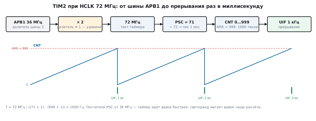
⚠️ Timers get twice the frequency of their APB bus if its divider is greater than one. With
HCLK= 72 MHz and APB1 = 36 MHz the timers count from 72 MHz, not from 36 (these are TIM2…TIM4 on APB1); APB2 on the F103 usually has no divider, and TIM1 counts from the same 72 MHz. On the F407 at 168 MHz both buses have a divider: APB1 = 42 MHz — the timers on it count from 84 MHz, APB2 = 84 MHz — TIM1, TIM8, TIM9…TIM11 count from 168 MHz. A calculation based on the bus frequency gives a result wrong by a factor of two — and this is probably the most common mistake when working with timers.
Always check it in practice: set a period of one second and look at the LED. If it blinks twice as fast, you have been caught.
13.4 Shadow registers
The mechanism that confuses people most.
PSC exists in two copies: the one you write to, and the one the timer
actually uses. The transfer from the first to the second happens on
the update event — that is, at the moment the counter overflows. ARR and CCR
work the same way, but their buffer is enabled separately — by preload: ARPE
for ARR, OCxPE for a channel. After reset preload is off, and a write
to ARR and CCR takes effect at once.
Why: if you change the period right in the middle of a period, the waveform is distorted. Shadow registers guarantee that the new value takes effect as a whole and at the boundary of a cycle.
Two consequences follow:
Settings are not applied immediately. You wrote PSC or, with preload
enabled, ARR, and the timer carries on
working the old way until the next overflow. If the period was long,
it looks as though "the setting did not work". To apply it forcibly,
generate an update event:
TIM3->EGR = TIM_EGR_UG; /* немедленно перенести значения в теневые регистры */
UG is a real update event: besides the transfer it clears the counter and
the prescaler and sets the UIF flag. If the update interrupt is already
enabled (UIE), the handler is called at once — hence the mysterious "extra"
interrupt at start-up; a flag left by UG will also trigger it later, at
the moment UIE is enabled. So UG is done before the interrupt is enabled and
the flag is cleared straight away: TIMx->SR = ~TIM_SR_UIF. Another way is to set
the URS bit in CR1 in advance: then UG transfers the values but does not set
the flag, and only overflows give an interrupt.
Preload must be enabled explicitly. For ARR this is the ARPE bit, for each
channel OCxPE. Without them a write goes straight through, and changing the duty in the middle
of a pulse gives a glitch. And reducing ARR on the fly without preload is dangerous:
if CNT is already greater than the new ARR, the counter counts up to 65 535, wraps
through zero, and one period comes out as long as 65 536 ticks.
13.5 🔧 PWM
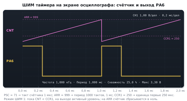
The most common use. The counter counts from zero to ARR, and the comparator
compares it with CCR: while CNT < CCR the output has one level, after that
the other.
частота ШИМ  = f_таймера / ((PSC + 1) × (ARR + 1))
заполнение   = CCR / (ARR + 1)
разрешение   = ARR + 1 градаций
The share of the period taken by the pulse is strictly called the duty cycle. In everyday Russian usage — and further in this handbook — it is called "skvazhnost", although strictly "skvazhnost" is the ratio of the period to the pulse width, T/τ: at a 25 % duty cycle it equals 4.
void tim3_pwm_init(uint16_t period, uint16_t duty)
{
    RCC->APB1ENR |= RCC_APB1ENR_TIM3EN;
    RCC->APB2ENR |= RCC_APB2ENR_IOPAEN;

    /* PA6 — выход альтернативной функции, push-pull. */
    GPIOA->CRL &= ~(GPIO_CRL_MODE6 | GPIO_CRL_CNF6);
    GPIOA->CRL |= GPIO_CRL_MODE6;      /* 11 -> выход 50 МГц */
    GPIOA->CRL |= GPIO_CRL_CNF6_1;     /* 10 -> альтернативная функция */

    TIM3->PSC = 72u - 1u;              /* тик 1 мкс */
    TIM3->ARR = period - 1u;
    TIM3->CCR1 = duty;

    /* Режим ШИМ 1: пока CNT < CCR — активный уровень. */
    TIM3->CCMR1 &= ~TIM_CCMR1_OC1M;
    TIM3->CCMR1 |= TIM_CCMR1_OC1M_2 | TIM_CCMR1_OC1M_1;   /* 110 */
    TIM3->CCMR1 |= TIM_CCMR1_OC1PE;    /* предзагрузка CCR1 */

    TIM3->CCER |= TIM_CCER_CC1E;       /* выход канала разрешён */

    TIM3->CR1 |= TIM_CR1_ARPE;
    TIM3->EGR = TIM_EGR_UG;            /* применить настройки немедленно */
    TIM3->CR1 |= TIM_CR1_CEN;
}
After that the duty is changed with one line: TIM3->CCR1 = новое_значение;
For example, tim3_pwm_init(1000, 250) gives 1 kHz and a 25 % duty. This is how it looks on an oscilloscope;
the timer does not output the counter sawtooth — it is drawn above the output for clarity:
The trade-off between frequency and resolution. The product of frequency and the number of steps is limited by the clock:
| PWM frequency | ARR at 72 MHz without division |
Steps |
|---|---|---|
| 1 kHz | 71 999 (does not fit in 16 bits) | a prescaler is needed |
| 20 kHz | 3599 | 3600 — plenty |
| 100 kHz | 719 | 720 |
| 1 MHz | 71 | 72 — rather coarse |
For motor control 20 kHz is used (above the audible range) and gives excellent resolution. For LED backlighting 500 Hz is enough — the eye will not notice.
The "PWM" tab in the app's calculators computes the frequency, duty and number of steps from PSC, ARR and CCR, and for a required frequency — ARR without a prescaler and CCR for the required duty.
⚠️ TIM1 and TIM8 have a main output switch. Everything is set up correctly, the counter runs,
CCRchanges — and the pin is silent. The reason is theMOEbit of theBDTRregister, which is cleared by default:
c
TIM1->BDTR |= TIM_BDTR_MOE;
TIM2…TIM5 and TIM9…TIM14 have no such register at all, so code debugged on TIM3 silently stops working when moved to TIM1. The
MOEbit also exists on TIM15, TIM16 and TIM17 (F0, G0, F3, L4 and other series): their PWM is also enabled throughBDTR.
13.6 Input capture
The reverse task: not generating a signal but measuring one. On an edge at the input the timer
copies the current counter value into CCR — you get an exact timestamp
without involving the processor.
void tim4_capture_init(void)
{
    RCC->APB1ENR |= RCC_APB1ENR_TIM4EN;

    TIM4->PSC = 72u - 1u;              /* тик 1 мкс */
    TIM4->ARR = 0xFFFFu;               /* считаем до предела */
    TIM4->EGR = TIM_EGR_UG;            /* PSC вступает в силу сразу (13.4) */

    /* Канал 1 переключается на ВХОД. */
    TIM4->CCMR1 &= ~TIM_CCMR1_CC1S;
    TIM4->CCMR1 |= TIM_CCMR1_CC1S_0;   /* 01 -> вход TI1 */

    TIM4->CCER &= ~TIM_CCER_CC1P;      /* нарастающий фронт */
    TIM4->CCER |= TIM_CCER_CC1E;

    TIM4->DIER |= TIM_DIER_CC1IE;
    TIM4->CR1 |= TIM_CR1_CEN;

    NVIC_EnableIRQ(TIM4_IRQn);
}
The difference between two consecutive stamps gives the signal period, and hence the frequency.
Measuring the duty is done with two channels at once: one catches the rising edge, the other the falling edge, both tied to the same input. This is a separate mode — PWM input, and the timer sets it up almost automatically.
Typical uses: frequency measurement, decoding signals from distance sensors, receiving signals from remote controls and radio receivers.
13.7 Encoder
The timer can count the pulses of a rotary encoder by itself, working out
the direction from two phase-shifted signals. The processor does not take part at all —
it just reads CNT when needed.
It is set up with slave mode in SMCR: counting on one channel, on the other
or on both at once. The last option gives four times the resolution.
The encoder together with PWM in practice — in 13.10.
A practical detail: the counter is 16‑bit and overflows. For an encoder turned in one direction for a long time you need to catch the overflow with an interrupt and keep the high part of the count in software — or take the 32‑bit TIM2/TIM5 on the F4.
13.8 One-pulse mode
The timer produces exactly one pulse of the given width and stops. Convenient for generating a strobe, the trigger pulse of an ultrasonic sensor, a delayed signal.
It is enabled by the OPM bit in CR1: after the first update event the counter
switches itself off.
13.9 Synchronising several timers
Timers can control one another: one becomes the master and, on its
event, starts, stops or clocks the slave. This is configured with a pair
of registers — CR2 in the master (what exactly to output) and SMCR
in the slave (how to react).
What it is for:
- cascading counters — getting around the 16‑bit limit on the F1 by obtaining a 32‑bit count from two timers;
- synchronous start of several PWM channels so that the phases do not drift apart;
- an exact delay between two events;
- triggering the ADC from a timer — the most common case, covered in section 14.
13.10 🔧 Brightness from an encoder
You turn the knob — the LED smoothly gets brighter or dimmer. Here the encoder (13.7), PWM (13.5) and the way the eye perceives brightness (57.3) come together. Both timers work by themselves; the processor is left with one line in the loop.
| F103 (BluePill) | F407 (Discovery) | |
|---|---|---|
| encoder | TIM2: PA0, PA1 | TIM3: PB4, PB5 (AF2) |
| PWM | TIM3, channel 1: PA6 | TIM4, channel 1: PD12 (AF2) — the board's green LED |
| PWM tick 1 µs | PSC = 71 at 72 MHz |
PSC = 83 at 84 MHz |
The BluePill LED on PC13 is not connected to a timer, and PWM on it is only possible in software — you need an external LED with a resistor on PA6. The encoder contacts short the pins to ground, so the inputs have pull-ups.
void enc_pwm_init(void)
{
    pins();

    /* энкодер: оба канала — входы с самым длинным фильтром, счёт по обоим фронтам */
    ENC->CCMR1 = TIM_CCMR1_CC1S_0 | TIM_CCMR1_CC2S_0 | TIM_CCMR1_IC1F | TIM_CCMR1_IC2F;
    ENC->SMCR  = TIM_SMCR_SMS_1 | TIM_SMCR_SMS_0;             /* 011: энкодер, ×4 */
    ENC->ARR   = 0xFFFFu;
    ENC->CR1   = TIM_CR1_CKD_1 | TIM_CR1_CEN;                 /* f_DTS = f / 4 — для фильтра */

    /* ШИМ: 1 кГц, 1000 градаций */
    PWM->PSC   = PWM_PSC;
    PWM->ARR   = 999u;
    PWM->CCMR1 = TIM_CCMR1_OC1M_2 | TIM_CCMR1_OC1M_1 | TIM_CCMR1_OC1PE;   /* ШИМ 1, предзагрузка */
    PWM->CCER  = TIM_CCER_CC1E;
    PWM->CR1   = TIM_CR1_ARPE;
    PWM->EGR   = TIM_EGR_UG;
    PWM->CR1  |= TIM_CR1_CEN;

    brightness_reset((uint16_t)ENC->CNT);
}

int main(void)
{
    enc_pwm_init();
    for (;;)
        PWM->CCR1 = brightness_step((uint16_t)ENC->CNT);
}
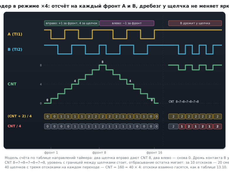
Counting. In encoder mode on both channels the timer catches both edges of both
signals — four counts per full cycle. In common mechanical
encoders a full cycle is one detent, so a detent gives four
counts; on some models a detent is half a cycle, and then two. The timer determines
the direction itself: CNT grows when turned one way and decreases the other way.
Bounce. The longest input filter is 8 samples at f_DTS / 32;
at 72 MHz and CKD = ÷4 this is 8 / (18 MHz / 32) ≈ 14 µs. Contact bounce lasts
milliseconds, and the filter will not remove it, but bounce does not hurt a quadrature count:
while one contact bounces, the other stays still, and the count goes +1 −1 in place.
The brightness level changes midway between detents — (отсчёты + 2) / 4.
A knob released on a detent sits two counts away from a level boundary, and a contact
bouncing at the edge does not make the brightness jump.
Passing through zero. Turn the knob left from the start — CNT becomes
65535, 65534… If CNT is taken as the position, the brightness jumps to maximum.
The right way is to take the signed difference of readings: (int16_t)(uint16_t)(cnt - s_last)
is correct across the wrap too, as long as there are fewer than 32 768 counts between reads. The accumulated
value is clamped on both sides: a knob that has hit the end responds
to turning back at once, without winding off extra turns.
#define STEPS 32                    /* уровней яркости */
#define PER   4                     /* отсчётов на щелчок: оба фронта обоих каналов */

/* round(1000 · (i / 31)^2,2); при ARR = 999 значение 1000 — горит постоянно */
static const uint16_t gamma22[STEPS] = {
       0,    1,    2,    6,   11,   18,   27,   38,   51,   66,   83,
     102,  124,  148,  174,  202,  233,  267,  302,  341,  381,  425,
     470,  519,  569,  623,  679,  738,  799,  864,  930, 1000,
};

static uint16_t s_last;             /* прошлое показание CNT */
static int32_t  s_acc;              /* отсчёты от нижнего края: 0 … PER·(STEPS−1) */

uint16_t brightness_step(uint16_t cnt)
{
    int32_t acc = s_acc + (int16_t)(uint16_t)(cnt - s_last);   /* верно и через 0 ↔ 65535 */
    s_last = cnt;
    if (acc < 0)
        acc = 0;                                /* упёрлись — обратный поворот */
    if (acc > PER * (STEPS - 1))                /* откликается сразу */
        acc = PER * (STEPS - 1);
    s_acc = acc;
    return gamma22[(acc + PER / 2) / PER];      /* граница уровня — между щелчками */
}
The scale. 32 levels along a gamma of 2.2 (why not linear — in 57.3). The top
value 1000 = ARR + 1: the LED is on continuously (13.12). The first steps are
1, 2 and 6 out of 1000, which the eye sees as 4.3 %, 5.9 % and 9.8 % brightness. From zero
to full brightness takes 31 detents: with 20 detents per turn that is one and a half turns.
What the model showed. The encoder was modelled on a computer: a 16-bit count on both edges, three bounces on every contact transition, the brightness recomputed after every edge.
| What we did | CNT |
Level |
|---|---|---|
| 40 detents right | 160 = 40 × 4 | 31 — at the end stop |
| 5 detents back | 140 | 26 — responds at once |
| 2 right, the contact at the detent bounces 10 times | 148 | 28, not a single change |
| from zero 3 detents left | 65 524 | 0, not maximum |
| and 1 right | 65 528 | 1 |
If the level were computed by dropping the remainder (отсчёты / 4), the same bounce
at the detent would give 20 brightness changes.
Blinking with no program at all. The same PWM with a period of one second blinks by itself:
a tick of 0.1 ms (PSC = 7199 on the F103, 8399 on the F407), ARR = 9999 — a 1 s period,
CCR1 = 2500 — on for 250 ms. For comparison: toggling a pin in an interrupt
every 0.5 s gives blinking at 1 Hz, not 2 — a full period consists of two
toggles.
13.11 F0 and G0: the same timers, other clock names
Timers are the part of the STM32 that hardly changes from series to series:
CR1, PSC, ARR at 0x2C, CCR1 at 0x34, capture and compare modes,
shadow registers — all as on the F1. The PWM recipe from 13.5 carries over to the F0
and G0 with two changes: the name of the clock enable register and the prescaler for
their frequency.
| F1 | F0 | G0 | |
|---|---|---|---|
| TIM3 clock | APB1ENR |
APB1ENR |
APBENR1 |
| TIM1 clock | APB2ENR |
APB2ENR |
APBENR2 |
TIM3_CH1 on PA6 |
AF mode in CRL |
AF1 | AF1 |
| timer clock at maximum | 72 MHz | 48 MHz | 64 MHz |
PSC for a 1 MHz count |
71 | 47 | 63 |
F1/F0 code with RCC->APB1ENR does not build on the G0: no member named 'APB1ENR'
in 'RCC_TypeDef'. 1 kHz PWM on the G0:
    RCC->APBENR1 |= RCC_APBENR1_TIM3EN;                                  /* у G0 — APBENR1 */
    GPIOA->AFR[0] = (GPIOA->AFR[0] & ~(0xFu << 24)) | (1u << 24);       /* PA6 -> AF1 = TIM3_CH1 */
    GPIOA->MODER = (GPIOA->MODER & ~(3u << 12)) | (2u << 12);
    TIM3->PSC = PSC_VAL;
    TIM3->ARR = ARR_VAL;
    TIM3->CCR1 = 250u;
    TIM3->CCMR1 = TIM_CCMR1_OC1M_2 | TIM_CCMR1_OC1M_1 | TIM_CCMR1_OC1PE;
    TIM3->CCER = TIM_CCER_CC1E;
    TIM3->CR1 = TIM_CR1_ARPE | TIM_CR1_CEN;
The set of timers depends on the chip. On the F072 and G071, on which the listings were
checked, these are the advanced TIM1 (with BDTR and the MOE bit, without which
the outputs are silent — 13.5), TIM2, TIM3, the basic TIM6 and TIM7 and the small
TIM14–TIM17; TIM15–TIM17 also have BDTR with MOE, and without this
bit their outputs are just as silent. TIM2 in both series is 32-bit: the counter
and ARR in the chip description are two 16-bit fields.
On the F1, for 1 kHz at the full clock, ARR "did not fit in 16 bits" (13.5), while
here it fits in any timer without a prescaler: ARR = 47 999 on the F0 and
63 999 on the G0 — less than 65 535. The 32 bits of TIM2 are needed for longer periods:
a 16-bit counter without a prescaler lasts only 1.37 ms at 48 MHz and
1.02 ms at 64 MHz, while TIM2 without one can count a whole second. But the F030,
F070, G030 and G070 have no TIM2 at all, and the F030x6, F070x6 and G030 also lack
TIM6 and TIM15: there a long period can only be obtained with the prescaler.
The exact set is in the feature table of the chip's datasheet.
13.12 Pitfalls
The frequency is twice what was expected. The doubling of the timer frequency on an APB bus with a divider greater than 1 was not taken into account.
Settings do not take effect. No update event (UG) was generated:
PSC, and with preload enabled also ARR and CCR, wait for it.
An interrupt came right after start. It was triggered by the UIF flag
set by writing UG: clear the flag after UG or set
URS in CR1 in advance (13.4).
One period is suddenly tens of times longer. ARR was reduced on the fly without
preload, and CNT ended up above the new value: the counter went up to 65 535
and wrapped through zero. Enable ARPE.
TIM1 is silent. MOE in BDTR is not set. TIM8
and TIM15…TIM17 are silent in the same way.
The flag is cleared incorrectly. For a timer you write zero, not one.
And TIM->SR = 0 also erases the flags of all channels — the right way is
TIM->SR = ~TIM_SR_UIF.
The pin is not configured for the alternate function. The timer runs, CCR
changes, but the pin stays an ordinary GPIO and outputs nothing.
Overflow during capture. If the signal period is longer than a full counter cycle, the difference of stamps is meaningless. Count overflows or increase the prescaler.
Zero duty. CCR = 0 gives a constant inactive level,
CCR > ARR a constant active one. This is not a fault but normal behaviour,
but when calculating percentages it is easy to get CCR equal to ARR + 1
and be surprised that the PWM has disappeared.
The timer interrupt does not come. HAL_TIM_Base_Start only starts
counting; the update interrupt is enabled by HAL_TIM_Base_Start_IT — it sets
the UIE bit in DIER.
It blinks twice as slowly as calculated. Toggling every 0.5 s is a 1 s period, that is 1 Hz (13.10).
The brightness jumps to maximum when turning left. CNT was taken as the position
and wrapped through zero. You need the signed difference of readings (13.10).
The BluePill LED does not respond to PWM. Pin PC13 is not connected to a timer.
HAL_GetTick for short intervals. It counts milliseconds — a shorter interval
cannot be measured. For microseconds take a free timer with a 1 µs tick or
DWT->CYCCNT (section 73).
13.13 Summary
- Event frequency =
f / ((PSC + 1) × (ARR + 1)); the prescaler is taken as small as possible so thatARRis larger — that is the PWM resolution. - Timers on an APB bus with a divider greater than 1 get twice its frequency; on the F4 this also applies to APB2: TIM1 and TIM8 at 168 MHz count from 168 MHz.
PSCis always buffered,ARRandCCRonly with preload (ARPE,OCxPE; it is off after reset): then new values take effect on the update event, or forcibly by writingUGtoEGR.- Timer flags are cleared by writing zero, and preferably with a mask rather than zero to the whole register.
- On TIM1 and TIM8 (and TIM15…TIM17 where they exist) the outputs are enabled
by the
MOEbit; without it everything is configured but the pin is silent. - Capture gives timestamps of edges without the processor — hence frequency and duty measurement.
- The timer counts an encoder by itself, including direction: on both channels four
counts per full cycle, and bounce does not hurt the count. The position is the signed difference
of readings, not
CNTitself; the brightness scale follows a gamma curve (13.10). - You can blink with no program at all: PWM with a period of one second.
- On the F4, TIM2 and TIM5 are 32‑bit, which removes the need for cascades.
Full sources
tim_f0.c — 1 kHz PWM on TIM3 of the STM32F072.
/* Раздел 13.11: ШИМ 1 кГц на TIM3 канал 1 (PA6, AF1) у STM32F072 — таймер как у F1. */
#include <stddef.h>
#include "stm32f0xx.h"

_Static_assert(offsetof(TIM_TypeDef, ARR) == 0x2Cu && offsetof(TIM_TypeDef, CCR1) == 0x34u, "регистры как у F1");
#define TIM_HZ 48000000u                        /* такт таймера = PCLK 48 МГц (делитель APB 1) */
#define PSC_VAL 47u
#define ARR_VAL 999u
_Static_assert(TIM_HZ / (PSC_VAL + 1u) == 1000000u && TIM_HZ / (PSC_VAL + 1u) / (ARR_VAL + 1u) == 1000u, "1 МГц счёт, 1 кГц ШИМ");

void pwm_init_f0(void)
{
    RCC->AHBENR |= RCC_AHBENR_GPIOAEN;
    RCC->APB1ENR |= RCC_APB1ENR_TIM3EN;
    GPIOA->AFR[0] = (GPIOA->AFR[0] & ~(0xFu << 24)) | (1u << 24);       /* PA6 -> AF1 = TIM3_CH1 */
    GPIOA->MODER = (GPIOA->MODER & ~(3u << 12)) | (2u << 12);
    TIM3->PSC = PSC_VAL;
    TIM3->ARR = ARR_VAL;
    TIM3->CCR1 = 250u;                          /* 25 % */
    TIM3->CCMR1 = TIM_CCMR1_OC1M_2 | TIM_CCMR1_OC1M_1 | TIM_CCMR1_OC1PE;   /* PWM1, с буфером */
    TIM3->CCER = TIM_CCER_CC1E;
    TIM3->CR1 = TIM_CR1_ARPE | TIM_CR1_CEN;
}
tim_g0.c — the same PWM on the STM32G071.
/* Раздел 13.11: тот же ШИМ на STM32G071 — TIM3 канал 1 (PA6, AF1), такт с APBENR1, 64 МГц. */
#include <stddef.h>
#include "stm32g0xx.h"

_Static_assert(offsetof(TIM_TypeDef, ARR) == 0x2Cu && offsetof(TIM_TypeDef, CCR1) == 0x34u, "регистры как у F0 и F1");
#define TIM_HZ 64000000u
#define PSC_VAL 63u
#define ARR_VAL 999u
_Static_assert(TIM_HZ / (PSC_VAL + 1u) == 1000000u && TIM_HZ / (PSC_VAL + 1u) / (ARR_VAL + 1u) == 1000u, "1 МГц счёт, 1 кГц ШИМ");

void pwm_init_g0(void)
{
    RCC->IOPENR |= RCC_IOPENR_GPIOAEN;
    RCC->APBENR1 |= RCC_APBENR1_TIM3EN;                                  /* у G0 — APBENR1 */
    GPIOA->AFR[0] = (GPIOA->AFR[0] & ~(0xFu << 24)) | (1u << 24);       /* PA6 -> AF1 = TIM3_CH1 */
    GPIOA->MODER = (GPIOA->MODER & ~(3u << 12)) | (2u << 12);
    TIM3->PSC = PSC_VAL;
    TIM3->ARR = ARR_VAL;
    TIM3->CCR1 = 250u;
    TIM3->CCMR1 = TIM_CCMR1_OC1M_2 | TIM_CCMR1_OC1M_1 | TIM_CCMR1_OC1PE;
    TIM3->CCER = TIM_CCER_CC1E;
    TIM3->CR1 = TIM_CR1_ARPE | TIM_CR1_CEN;
}
Next: section 13а "Servo: 50 Hz PWM, 1–2 ms pulse, angle, smooth motion and power".