 Embedded HandbookApps
48д. The ST factory bootloader in system memory: entry via BOOT0 and from firmware, the USART protocol, your own flashing utility
In section 4.9 the factory bootloader appeared as a way to rescue a board: BOOT0
to one, a reset — and the chip waits for firmware over USART1. In 48.11 it comes
first among the ready-made update paths. Sections 48а–48г and 198щ built our own
bootloader: signature, MCUboot, delta update, encryption. Here we look at the
bootloader that already sits in every chip and that you do not have to write.
The section covers: what system memory is and when the factory bootloader is enough;
how to get into it with the BOOT0 pin on F1 and F4 and with the nBOOT0 and
nSWBOOT0 bits on G4; how to jump into it from running firmware — our own C code
for three families; which interfaces and pins the F103C8, F407 and G474 have;
the USART protocol per AN3155 — the frame of every command; our own flashing utility in
Python and the bootloader model it was tested against; pitfalls.
Sources: AN2606 Rev 21, DocID13801 (the factory bootloader of all families: table 2 — entry conditions, 3.1 — jump from firmware, table 3 — interfaces and versions, tables 6, 7 — F10xxx, tables 22–25 — F40xxx/41xxx, table 68 — PID and addresses, tables 69, 70 — startup time), public address — st.com, AN2606; AN3155 Rev 6, DocID17066 (USART protocol: commands, checksums, versions) — st.com, AN3155; RM0008 Rev 17 (F1: table 9 — boot modes, table 5 — pages), RM0090 Rev 19 (F4: table 2 — boot modes, table 5 — sectors, 3.7.3 — RDP levels), RM0440 Rev 6 and datasheet DS12288 Rev 5 (G4: table 5 — boot modes, 2.4 — RAM, 47.6.1 — device ID). The AN2606 revision this section was checked against came out before G4; newer revisions also describe G4, but the section was not checked against them — so on G4 this section says only what is in RM0440 and DS12288. License: the section's own code — free to use.
Terms used in the documentation
Term Meaning system memory boot mode booting from system memory bootloader activation pattern the set of conditions for entering the bootloader automatic baud rate detection detecting the baud rate from the first byte even parity (8E1) 8 data bits, even parity bit, 1 stop bit XOR checksum byte checksum byte: exclusive OR of all bytes of the block product ID (PID), Get ID the chip family number, the command that reads it bootloader ID the version number of the bootloader in system memory Erase / Extended Erase erasing with one-byte / two-byte page numbers Readout Protect / Readout Unprotect enable / remove readout protection Go command the "go" command: stack and entry point from the vector table physical remap (MEM_MODE) what is visible at address 0: Flash, system memory or RAM software BOOT0 (nSWBOOT0, nBOOT0) BOOT0 from the option bytes instead of the pin
48д.1 System memory, and when the factory bootloader beats your own
Besides the Flash for the program, an STM32 has an information block: the option
bytes and system memory with ST code written at the factory. You cannot erase
or rewrite it: per AN2606 (table 5) the Write and Erase commands do not work on
system memory, only Read. On F103 it is 2 KB from address
0x1FFFF000, on F407 — 0x1FFF0000…0x1FFF77FF (AN2606, table 68), on G474
— 28 KB from 0x1FFF0000 (RM0440, 2.6.1 and the Flash layout).
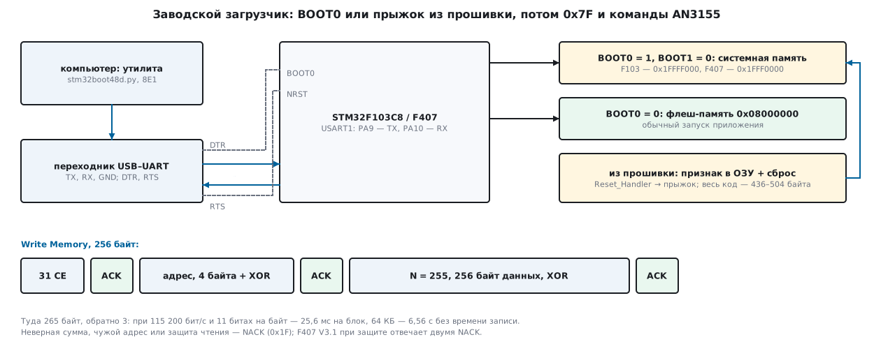
What the bootloader can do, the same for all families: receive an image over one of the interfaces, erase and write Flash, read it, enable and remove read and write protection, jump to an address. What it cannot do: check whose image it is (there is no signature), roll back to the previous version, receive an image over radio.
| When | Factory | Your own (48, 198щ) |
|---|---|---|
| flash a board on the desk without a programmer | yes | — |
revive a board where the program took over PA13/PA14 (4.9) |
yes | — |
| programming on a production line over UART | yes | possible |
| update at the customer's site over a UART or USB brought outside | yes, if no signature is needed | yes |
| signature, encryption, rollback, log (48а–48г, 198щ) | no | yes |
| update over Bluetooth, radio, network | no | yes |
| Flash space used | 0 bytes | 4528 bytes for 198щ |
There is one more reason to keep the factory bootloader in mind even when you have your
own: it always stays in the chip. Whoever can set BOOT0 to
one and connect to USART1 can read the Flash — if
readout protection is not enabled (11в), and can erase it and write their own — always, except on
F4 and G4 with RDP level 2: there entry into system memory is closed (RM0090, 3.7.3;
RM0440, p. 123).
48д.2 Entry via pins: BOOT0 and BOOT1, nBOOT0 and nSWBOOT0
On F1 and F4 the boot area is selected by two pins (RM0008, table 9; RM0090,
table 2): BOOT0 = 0 — Flash, BOOT0 = 1 and BOOT1 = 0 — system
memory, both at one — RAM. The values are latched on the 4th rising edge of the
SYSCLK clock after reset and again on exit from Standby, so you have to hold them all that time.
In AN2606 this is condition "pattern1" (table 2); on F10xxx and F40xxx/41xxx
the bootloader is entered exactly this way (4.1 and 11.1.1).
G4 has no BOOT1 pin; instead there is the nBOOT1 bit in FLASH_OPTR, and BOOT0
can be taken not from the PB8 pin but from the nBOOT0 bit (RM0440, table 5):
nSWBOOT0 |
BOOT0 source |
System memory when |
|---|---|---|
| 1 | pin PB8 |
PB8 = 1 and nBOOT1 = 1 |
| 0 | bit nBOOT0 |
nBOOT0 = 0 and nBOOT1 = 1 |
The BOOT_LOCK bit = 1 overrides everything: boot from Flash only. With
nSWBOOT0 = 0 the PB8 pin is freed as an ordinary pin — but then you can no longer
enter the bootloader with a pin: only by rewriting the option bytes or
by a jump from firmware (48д.3). The DS12288 datasheet calls the same bit
nBOOT_SEL, RM0440 calls it nSWBOOT0; they are one and the same.
A handy trick for BluePill and F4 with a USB–UART adapter: DTR drives BOOT0,
RTS drives NRST. The utility sets BOOT0, pulses reset, waits for the
bootloader to start and begins the exchange (enter_bootloader in 48д.6). How long to wait —
AN2606, table 69: on F10xxx at least 1.227 ms, on F40xxx/41xxx — 84.59 ms
for version V3.x and 74 ms for V9.x; the utility waits 0.1 s.
48д.3 Entry from running firmware
In a device inside an enclosure you cannot reach BOOT0. Then the application itself goes into
system memory — on a menu command, on a frame from the computer. AN2606 (3.1)
lists what to do before the jump: turn off the peripheral clocks and the PLL,
disable interrupts and clear pending requests. The bootloader expects
to find the chip in the state a reset leaves it in — the hand-over of control in
48.5 relies on the same condition.
The most reliable way is to restore nothing by hand but to really reset
the chip: the application puts a flag in RAM (as in 48.6 and 198щ.4 — a magic value and its
complement) and does a software reset; the first line of Reset_Handler, before
.data, .bss and clock setup, checks the flag — and jumps. The reset
restored everything by itself. The second way is a jump without a reset, when you cannot insert a check at the start of
Reset_Handler (the startup code is someone else's): then the code
stops SysTick, NVIC, the clocks and the peripherals itself.
All the code is one file for three families; register addresses are our own
#defines (checked against the CMSIS headers by the section's check):
/* sysboot48d.h — раздел 48д: вход в заводской загрузчик ST из работающей прошивки.
 * Собирать с -DSB_F1 (STM32F103), -DSB_F4 (STM32F407) или -DSB_G4 (STM32G474). */
#ifndef SYSBOOT48D_H
#define SYSBOOT48D_H
#include <stdint.h>

#if defined(SB_F1)
#define SB_SYSMEM_ADDR 0x1FFFF000u   /* AN2606, таблица 68 */
#define SB_FLAG_ADDR   0x20004FF0u   /* F103C8: 20 КБ ОЗУ, последние 16 байт (48.6) */
#elif defined(SB_F4)
#define SB_SYSMEM_ADDR 0x1FFF0000u   /* AN2606, таблица 68 */
#define SB_FLAG_ADDR   0x2001FFF0u   /* F407: 128 КБ основного ОЗУ */
#elif defined(SB_G4)
#define SB_SYSMEM_ADDR 0x1FFF0000u   /* RM0440, 2.6.1 */
#define SB_FLAG_ADDR   0x20017FF0u   /* G474: SRAM1 80 КБ + SRAM2 16 КБ (RM0440, 2.4) */
#else
#error "SB_F1, SB_F4 или SB_G4"
#endif

#ifndef SB_SYSMEM
#define SB_SYSMEM SB_SYSMEM_ADDR     /* опыт в QEMU подставляет свой адрес */
#endif

#define SB_MAGIC 0x5B007ED0u

void sysboot_request(void);    /* из приложения: признак в ОЗУ и программный сброс */
void sysboot_early(void);      /* первой строкой Reset_Handler, до .data, .bss и тактирования */
void sysboot_jump_now(void);   /* без сброса: вернуть камень к состоянию после сброса и прыгнуть */

#endif
/* sysboot48d.c — раздел 48д: вход в заводской загрузчик ST из работающей прошивки, без вывода BOOT0.
 * Два пути. Надёжный: признак в ОЗУ + программный сброс, а после сброса — прыжок первой строкой
 * Reset_Handler, пока ничего не включено. Быстрый: прыжок сразу, вернув камень к состоянию после сброса
 * так, как велит AN2606, 3.1: такты периферии выключить, PLL выключить, прерывания запретить и снять.
 * Адреса регистров — из RM0008, RM0090, RM0440; сверены с заголовками CMSIS проверкой раздела. */
#include "sysboot48d.h"

#define REG(a) (*(volatile uint32_t *)(a))

/* Ядро Cortex-M3/M4 — одинаково у всех трёх семейств */
#define SYST_CSR     REG(0xE000E010u)
#define SYST_RVR     REG(0xE000E014u)
#define SYST_CVR     REG(0xE000E018u)
#define NVIC_ICER(i) REG(0xE000E180u + 4u * (i))
#define NVIC_ICPR(i) REG(0xE000E280u + 4u * (i))
#define SCB_ICSR     REG(0xE000ED04u)
#define SCB_VTOR     REG(0xE000ED08u)
#define SCB_AIRCR    REG(0xE000ED0Cu)
#define ICSR_PENDSTCLR (1u << 25)
#define AIRCR_RESET  (0x05FA0000u | (1u << 2))   /* ключ VECTKEY и SYSRESETREQ */

#if defined(SB_F1)
#define RCC          0x40021000u
#define RCC_CR       REG(RCC + 0x00u)
#define RCC_CFGR     REG(RCC + 0x04u)
#define RCC_CIR      REG(RCC + 0x08u)
#define RCC_APB2RSTR REG(RCC + 0x0Cu)
#define RCC_APB1RSTR REG(RCC + 0x10u)
#define RCC_AHBENR   REG(RCC + 0x14u)
#define RCC_APB2ENR  REG(RCC + 0x18u)
#define RCC_APB1ENR  REG(RCC + 0x1Cu)
#define DMA1_CCR(ch) REG(0x40020008u + 20u * (ch))   /* каналы 1…7: ch = 0…6 */
#define CR_HSION     (1u << 0)
#define CR_HSIRDY    (1u << 1)
#define CFGR_SW_HSI  0x0u
#define CFGR_RESET   0x00000000u
#elif defined(SB_F4)
#define RCC          0x40023800u
#define RCC_CR       REG(RCC + 0x00u)
#define RCC_CFGR     REG(RCC + 0x08u)
#define RCC_CIR      REG(RCC + 0x0Cu)
#define RCC_AHB1RSTR REG(RCC + 0x10u)
#define RCC_AHB2RSTR REG(RCC + 0x14u)
#define RCC_AHB3RSTR REG(RCC + 0x18u)
#define RCC_APB1RSTR REG(RCC + 0x20u)
#define RCC_APB2RSTR REG(RCC + 0x24u)
#define RCC_AHB1ENR  REG(RCC + 0x30u)
#define RCC_AHB2ENR  REG(RCC + 0x34u)
#define RCC_AHB3ENR  REG(RCC + 0x38u)
#define RCC_APB1ENR  REG(RCC + 0x40u)
#define RCC_APB2ENR  REG(RCC + 0x44u)
#define SYSCFG_MEMRMP REG(0x40013800u)
#define APB2ENR_SYSCFGEN (1u << 14)
#define CR_HSION     (1u << 0)
#define CR_HSIRDY    (1u << 1)
#define CFGR_SW_HSI  0x0u
#define CFGR_RESET   0x00000000u
#elif defined(SB_G4)
#define RCC          0x40021000u
#define RCC_CR       REG(RCC + 0x00u)
#define RCC_CFGR     REG(RCC + 0x08u)
#define RCC_CIER     REG(RCC + 0x18u)
#define RCC_AHB1RSTR REG(RCC + 0x28u)
#define RCC_AHB2RSTR REG(RCC + 0x2Cu)
#define RCC_AHB3RSTR REG(RCC + 0x30u)
#define RCC_APB1RSTR1 REG(RCC + 0x38u)
#define RCC_APB1RSTR2 REG(RCC + 0x3Cu)
#define RCC_APB2RSTR REG(RCC + 0x40u)
#define RCC_AHB1ENR  REG(RCC + 0x48u)
#define RCC_AHB2ENR  REG(RCC + 0x4Cu)
#define RCC_AHB3ENR  REG(RCC + 0x50u)
#define RCC_APB1ENR1 REG(RCC + 0x58u)
#define RCC_APB1ENR2 REG(RCC + 0x5Cu)
#define RCC_APB2ENR  REG(RCC + 0x60u)
#define SYSCFG_MEMRMP REG(0x40010000u)
#define APB2ENR_SYSCFGEN (1u << 0)
#define AHB1RSTR_FLASHRST (1u << 8)      /* флеш-память не сбрасываем: из неё идёт этот код */
#define CR_HSION     (1u << 8)
#define CR_HSIRDY    (1u << 10)
#define CFGR_SW_HSI  0x1u                /* у G4 HSI16 — это 01 */
#define CFGR_RESET   0x00000005u
#endif

#define CR_HSEON     (1u << 16)
#define CR_CSSON     (1u << 19)
#define CR_PLLON     (1u << 24)
#define CFGR_SW      0x3u
#define CFGR_SWS     (0x3u << 2)
#define SB_WAIT      100000u             /* ожидания с пределом: зависший генератор не вешает прыжок */

#define SB_FLAG ((volatile uint32_t *)SB_FLAG_ADDR)

__attribute__((noreturn)) static void sb_jump(uint32_t base)
{
    uint32_t sp = REG(base);
    uint32_t pc = REG(base + 4u);

    __asm volatile("msr msp, %0\n"
                   "msr control, %1\n"   /* стек MSP, привилегированный режим, без следа FPU */
                   "isb\n"
                   "cpsie i\n"           /* после сброса PRIMASK = 0 — загрузчик ждёт именно этого */
                   "bx %2\n"
                   :
                   : "r"(sp), "r"(0u), "r"(pc)
                   : "memory");
    for (;;) {
    }
}

static void sb_remap(void)
{
#if defined(SB_F4) || defined(SB_G4)
    RCC_APB2ENR |= APB2ENR_SYSCFGEN;
    (void)RCC_APB2ENR;
    SYSCFG_MEMRMP = 0x1u;                /* MEM_MODE = 01: по адресу 0 — системная память */
#endif
    SCB_VTOR = SB_SYSMEM;
    __asm volatile("dsb\n"
                   "isb\n" ::: "memory");
}

void sysboot_request(void)
{
    SB_FLAG[0] = SB_MAGIC;
    SB_FLAG[1] = ~SB_MAGIC;
    __asm volatile("dsb" ::: "memory");
    SCB_AIRCR = AIRCR_RESET;
    __asm volatile("dsb" ::: "memory");
    for (;;) {
    }
}

void sysboot_early(void)
{
    if (SB_FLAG[0] != SB_MAGIC || SB_FLAG[1] != ~SB_MAGIC)
        return;
    SB_FLAG[0] = 0u;                     /* прочитали — стёрли, иначе загрузчик навсегда */
    SB_FLAG[1] = 0u;
    sb_remap();
    sb_jump(SB_SYSMEM);
}

static void sb_clocks_reset(void)
{
    uint32_t n;

    RCC_CR |= CR_HSION;
    for (n = 0u; n < SB_WAIT && !(RCC_CR & CR_HSIRDY); n++) {
    }
    RCC_CFGR = (RCC_CFGR & ~CFGR_SW) | CFGR_SW_HSI;
    for (n = 0u; n < SB_WAIT && (RCC_CFGR & CFGR_SWS) != (CFGR_SW_HSI << 2); n++) {
    }
    RCC_CFGR = CFGR_RESET;               /* делители и MCO — как после сброса */
    RCC_CR &= ~(CR_PLLON | CR_CSSON);
    RCC_CR &= ~CR_HSEON;
#if defined(SB_G4)
    RCC_CIER = 0u;                       /* прерывания RCC выключены */
#else
    RCC_CIR = 0u;
#endif
}

static void sb_periph_reset(void)
{
#if defined(SB_F1)
    uint32_t ch;
    RCC_AHBENR |= 1u;                    /* DMA1EN: у F103 сброса DMA через RCC нет — гасим каналы сами */
    for (ch = 0u; ch < 7u; ch++)
        DMA1_CCR(ch) = 0u;
    RCC_APB2RSTR = 0xFFFFFFFFu;
    RCC_APB2RSTR = 0u;
    RCC_APB1RSTR = 0xFFFFFFFFu;
    RCC_APB1RSTR = 0u;
    RCC_AHBENR = 0x00000014u;            /* значения после сброса (RM0008, 7.3.6–7.3.8) */
    RCC_APB2ENR = 0u;
    RCC_APB1ENR = 0u;
#elif defined(SB_F4)
    RCC_AHB1RSTR = 0xFFFFFFFFu;
    RCC_AHB1RSTR = 0u;
    RCC_AHB2RSTR = 0xFFFFFFFFu;
    RCC_AHB2RSTR = 0u;
    RCC_AHB3RSTR = 0xFFFFFFFFu;
    RCC_AHB3RSTR = 0u;
    RCC_APB1RSTR = 0xFFFFFFFFu;
    RCC_APB1RSTR = 0u;
    RCC_APB2RSTR = 0xFFFFFFFFu;
    RCC_APB2RSTR = 0u;
    RCC_AHB1ENR = 0x00100000u;           /* значения после сброса (RM0090, 6.3.10–6.3.14) */
    RCC_AHB2ENR = 0u;
    RCC_AHB3ENR = 0u;
    RCC_APB1ENR = 0u;
    RCC_APB2ENR = 0u;
#elif defined(SB_G4)
    RCC_AHB1RSTR = ~AHB1RSTR_FLASHRST;
    RCC_AHB1RSTR = 0u;
    RCC_AHB2RSTR = 0xFFFFFFFFu;
    RCC_AHB2RSTR = 0u;
    RCC_AHB3RSTR = 0xFFFFFFFFu;
    RCC_AHB3RSTR = 0u;
    RCC_APB1RSTR1 = 0xFFFFFFFFu;
    RCC_APB1RSTR1 = 0u;
    RCC_APB1RSTR2 = 0xFFFFFFFFu;
    RCC_APB1RSTR2 = 0u;
    RCC_APB2RSTR = 0xFFFFFFFFu;
    RCC_APB2RSTR = 0u;
    RCC_AHB1ENR = 0x00000100u;           /* значения после сброса (RM0440, 7.4.14–7.4.19) */
    RCC_AHB2ENR = 0u;
    RCC_AHB3ENR = 0u;
    RCC_APB1ENR1 = 0x00000400u;
    RCC_APB1ENR2 = 0u;
    RCC_APB2ENR = 0u;
#endif
}

void sysboot_jump_now(void)
{
    uint32_t i;

    __asm volatile("cpsid i" ::: "memory");
    SYST_CSR = 0u;                       /* SysTick стоп: загрузчик меряет им скорость сам */
    SYST_RVR = 0u;
    SYST_CVR = 0u;
    SCB_ICSR = ICSR_PENDSTCLR;
    for (i = 0u; i < 8u; i++) {
        NVIC_ICER(i) = 0xFFFFFFFFu;      /* запретить все прерывания */
        NVIC_ICPR(i) = 0xFFFFFFFFu;      /* и снять висящие запросы */
    }
    sb_clocks_reset();
    sb_periph_reset();
    for (i = 0u; i < 8u; i++)
        NVIC_ICPR(i) = 0xFFFFFFFFu;      /* сброс периферии мог поднять запросы ещё раз */
    sb_remap();
    sb_jump(SB_SYSMEM);
}
Why it is done this way:
- The flag is in the last 16 bytes of RAM, at the same address for the application and the startup code (48.6): the linker section is shortened by 16 bytes. The ST bootloader itself occupies the start of RAM — 512 bytes on F10xxx (AN2606, table 6), 8 KB on F40xxx V3.x and 12 KB on V9.x (tables 22 and 24) — it does not reach the end of RAM. Read it — erase it, otherwise the device stays in the bootloader forever.
- Stack is MSP,
CONTROL= 0. If the application runs under an OS on PSP, the bootloader would start on a foreign stack. The sameCONTROL= 0 clears the floating-point trace on F4 and G4. Call the jump from ordinary code, not from an interrupt handler: otherwise the bootloader ends up inside an exception. PRIMASK= 0 beforebx. After reset interrupts are enabled; by this point the NVIC is fully disabled and SysTick is stopped — enabling interrupts is safe.- On F4 and G4 system memory is mapped at address 0 (
SYSCFG_MEMRMP,MEM_MODE= 01), andVTORis set to its start. AN2606 (3.1) recommends this for dual-bank chips, where the jump would otherwise return to the application; F1 has no such register, there onlyVTORis set. - Peripherals are reset with a pulse in the
…RSTRregisters, clocks with the reset values from the reference manuals: on F103AHBENR=0x14(clocking of SRAM and the Flash interface in sleep mode), on F407AHB1ENR=0x00100000, on G474AHB1ENR=0x100andAPB1ENR1=0x400. The DMA channels on F103 are stopped with theENbit — it has no way to reset DMA through RCC (48.5). On G4 theFLASHRSTbit inAHB1RSTRis not touched: this very code runs from Flash. - Waits have a limit. If HSI does not come up, the jump still happens instead of hanging.
Sizes (arm-none-eabi-gcc 12.2.1, -Os): the whole file is 436 bytes of code on F1, 504 on F4 and 464 on G4, no data and no .bss; of these sysboot_jump_now is 276, 304 and 272, sysboot_early is 76, 56 and 56 (on F4 and G4 it is accompanied by sb_remap — 60 and 52 bytes, on F1 it is inlined), sysboot_request is 52, sb_jump is 32 bytes. In QEMU 7.2.22
(netduinoplus2 — that is an STM32F405) instead of ST system memory there is our own
vector table at 0x08008000; its "bootloader" prints the state in which it received
the chip. The jump without a reset — from a mode with PSP, with SysTick running, with
the USART1 interrupt enabled and pending:
APP before: systick=irq iser1=0x00000020 ispr1=0x00000020
BOOT msp=0x2000eff8 control=0x00000000 primask=0x00000000 ipsr=0x00000000 syst_csr=0x00000000 iser1=0x00000000 ispr1=0x00000000 vtor=0x08008000 memrmp=0x00000000 flag0=0x00000000
CONTROL, PRIMASK, IPSR are zeros: thread mode, MSP stack, interrupts
enabled. SysTick is stopped, the USART1 interrupt is both disabled and cleared (it was
0x20 in both registers). The stack pointer is 0x2000F000 from the table minus
8 bytes pushed by the "bootloader" function itself. The path through a reset gave the
same result, and the flag was erased after the jump. SYSCFG_MEMRMP reads as zero in QEMU —
the QEMU model does not store this register, so the memory remap was not tested here.
48д.4 Interfaces by family and automatic baud rate detection
| STM32F103C8 | STM32F407 | STM32G474 | |
|---|---|---|---|
| USART protocol version | V2.2 | V3.1 | — |
| USART | USART1: PA9 TX, PA10 RX |
USART1: PA9/PA10; USART3: PB10/PB11 or PC10/PC11 |
USART (DS12288) |
| USB DFU | no | PA11/PA12, OTG FS |
yes (DS12288) |
| CAN | no | CAN2: PB5 RX, PB13 TX, 125 kbit/s |
— |
| I²C | no | on V9.x: I2C1 PB6/PB7, I2C2 PF1/PF0, I2C3 PA8/PC9 |
yes (DS12288) |
| SPI | no | on V9.x: SPI1 PA4–PA7, SPI2 PI0–PI3 |
yes (DS12288) |
| PID | 0x410 |
0x413 |
0x469 (DEV_ID, RM0440, 47.6.1) |
| system memory | 0x1FFFF000, 2 KB |
0x1FFF0000…0x1FFF77FF |
0x1FFF0000, 28 KB |
| bootloader RAM | 512 bytes | 8 KB (V3.x), 12 KB (V9.x) | — |
| bootloader clock | HSI, PLL at 24 MHz | HSI, PLL at 24 MHz (V3.x) or 60 MHz (V9.x); CAN and DFU — from a 4–26 MHz crystal | — |
The source for F103 and F407 is AN2606: table 3 (interfaces and versions), tables
6, 22, 24 (pins, clock, RAM), table 68 (PID and addresses). On F407 the bootloader
comes in two generations — V3.x with ID 0x31 and V9.x with ID 0x90;
the ID is stored in system memory at address 0x1FFF77DE and is read with the
Read Memory command. For G474 — only what is in DS12288 (3.7: USART, I²C, SPI,
USB DFU) and RM0440; the G474 in all memory sizes is category 3 (RM0440, table 1),
with DEV_ID 0x469. The pins of the G4 interfaces and their versions are in the newer
AN2606 revisions, which this section was not checked against.
On F407, CAN and DFU need a crystal that is a multiple of 1 MHz, from 4 to 26 MHz; the bootloader
measures its frequency itself with timer TIM11 (AN2606, table 22). USART
runs from the internal HSI, no crystal is needed.
Automatic baud rate detection. The bootloader does not know the baud rate in advance. It waits
on RX for the frame 0x7F — start bit, 0x7F, parity bit, stop bit — and measures
its duration with the SysTick timer; from that it configures the USART and replies 0x79
(AN3155, 1). 0x7F was not chosen by chance: the low 7 bits are ones, the top one is
zero; between the falling edge of the start bit and the falling edge of bit 7 there are exactly 8 bit
periods. Baud rates from 1200 to 115200 bit/s have been tested; the mismatch between
the baud rates must be less than 2.5% (AN3155, 2). Which edges exactly the bootloader
measures, AN3155 does not specify; the section's model measures from falling edge to falling edge.
48д.5 The USART protocol per AN3155
The UART frame is 8 bits, even parity, 1 stop bit (AN2606, tables 6 and 22).
Replies are one byte: ACK 0x79 or NACK 0x1F (AN3155, 3). Three
protections against errors: parity of every byte; a command is sent as a pair "code and its
complement" (XOR of the pair = 0xFF); address and data blocks end with a checksum
byte — the XOR of all bytes of the block, so the XOR of the block together with the checksum = 0.
The address is 4 bytes, most significant first.
| Command | Code | From the computer after ACK on the code | Chip reply |
|---|---|---|---|
| Get | 00 FF |
— | N = 11, version, 11 command codes, ACK |
| Get Version | 01 FE |
— | version, 00, 00, ACK |
| Get ID | 02 FD |
— | N = 1, PID (2 bytes, most significant first), ACK |
| Read Memory | 11 EE |
address + checksum; N − 1 and its complement | ACK, ACK, N bytes |
| Go | 21 DE |
address + checksum | ACK, jump |
| Write Memory | 31 CE |
address + checksum; N − 1, N bytes, XOR | ACK, ACK |
| Erase | 43 BC |
N − 1, N numbers of one byte, XOR; or FF 00 |
ACK |
| Extended Erase | 44 BB |
N − 1 (2 bytes), N numbers of 2 bytes, XOR; or FF FF 00 |
ACK |
| Write Protect | 63 9C |
N − 1, N sector numbers, XOR | ACK, reset |
| Write Unprotect | 73 8C |
— | ACK, reset |
| Readout Protect | 82 7D |
— | ACK, reset |
| Readout Unprotect | 92 6D |
— | erase of the whole memory, ACK, reset |
Limitations and details people trip over:
- No more than 256 bytes per read and per write: the length is sent as the byte N − 1 (AN3155, 3.4 and 3.6). The write address is a multiple of 4, the length is a multiple of 4 (AN2606, 3.4).
- Erase or Extended Erase — one of the two. Extended Erase appeared in
protocol version 3.0 and replaced Erase (AN3155, table 3). On F103 (V2.2)
it is Erase
0x43, on F407 (V3.1) — Extended Erase0x44. The utility looks at which code Get returned. Numbers in Extended Erase are two bytes, plus0xFFFF— everything,0xFFFEand0xFFFD— bank 1 and bank 2 (AN3155, 3.8). For F103 a "page" is 1 KB (RM0008, table 5), for F407 — a sector of 16, 64 or 128 KB (RM0090, table 5). - Under readout protection only Get, Get Version, Get ID and Readout Unprotect work, everything else gets NACK (AN3155, table 2). Removing the protection erases the whole Flash, and bootloader V2.2 also clears RAM (AN2606, table 7).
- Write Protect, Write Unprotect, Readout Protect and Readout Unprotect
end with a chip reset — after them,
0x7Fagain. A second Write Protect replaces the first one rather than adding to it (AN3155, 3.9). - Writing and erasing protected sectors pass without an error — there is an ACK, but the Flash has not changed (AN3155, 3.6–3.8). Without a read-back check you will not see this.
- Go takes the stack from the address and jumps to address + 4 (AN3155, 3.5). An address in system memory or option bytes gets NACK (since version 2.1).
0xFFFF0000on F2 and F4 is not memory but a setting: the supply voltage for writing (AN2606, table 4). By default F4 writes Flash byte by byte; writing03 FF FF FFenables word writes with a supply of 2.7–3.6 V.
48д.6 Your own flashing utility and a bootloader model
The utility is not tied to a serial port: the Stm32Boot class talks to
any object that has write, read (returns less on timeout)
and flush_input. The pyserial port is the SerialPort class; the bootloader model is
ModelPort. This way the same code works with a board and is tested on the
computer. In full:
# -*- coding: utf-8 -*-
"""stm32boot48d.py — раздел 48д: своя утилита прошивки через заводской загрузчик STM32 (протокол USART, AN3155).

Протокол не знает, что под ним: класс Stm32Boot работает с любым «портом» — объектом с методами
write(data), read(n) (вернёт меньше n байт по тайм-ауту), flush_input() и, по желанию, set_boot0(v),
set_reset(v). Порт на pyserial — SerialPort ниже; модель загрузчика — в model48d.py.
Запуск с настоящей платой (нужен pyserial):  python stm32boot48d.py COM5 firmware.bin [0x08000000]"""
import sys, time

ACK, NACK, SYNC = 0x79, 0x1F, 0x7F
GET, GV, GID, READ, GO, WRITE = 0x00, 0x01, 0x02, 0x11, 0x21, 0x31
ERASE, EXT_ERASE, WP, WUP, RP, RUP = 0x43, 0x44, 0x63, 0x73, 0x82, 0x92
# Раскладка флеш-памяти по номеру кристалла (PID из Get ID): F103 medium-density — страницы по 1 КБ
# (RM0008, таблица 5), F407 — секторы 16/16/16/16/64/128 × 7 КБ (RM0090, таблица 5).
LAYOUT = {
    0x410: ("страницы", [1024] * 128),
    0x413: ("секторы", [16384] * 4 + [65536] + [131072] * 7),
}


class BootError(Exception):
    pass


class Nack(BootError):
    pass


def xor(data):
    x = 0
    for b in data:
        x ^= b
    return x


class SerialPort:
    """Порт на pyserial: 8 бит, чётность even, 1 стоп (AN2606: так настроен USART загрузчика).
    DTR ведёт BOOT0, RTS — NRST; полярность зависит от переходника, поэтому её можно перевернуть."""

    def __init__(self, name, baud=115200, timeout=1.0, inv_boot0=False, inv_reset=False):
        import serial  # pyserial
        self.s = serial.Serial(name, baud, bytesize=8, parity=serial.PARITY_EVEN, stopbits=1, timeout=timeout)
        self.inv_boot0, self.inv_reset = inv_boot0, inv_reset

    def write(self, data):
        self.s.write(bytes(data))

    def read(self, n):
        return self.s.read(n)

    def flush_input(self):
        time.sleep(0.05)
        self.s.reset_input_buffer()

    def set_boot0(self, level):
        self.s.dtr = bool(level) != self.inv_boot0

    def set_reset(self, active):
        self.s.rts = bool(active) != self.inv_reset


class Stm32Boot:
    def __init__(self, port, echo=False):
        self.port = port
        self.echo = echo          # переходник возвращает каждый посланный байт (полудуплекс, один провод)
        self.tx = self.rx = 0     # байт в линии туда и обратно — для оценки времени
        self.version = None
        self.cmds = b""

    def _send(self, data):
        data = bytes(data)
        self.port.write(data)
        self.tx += len(data)
        if self.echo:
            back = self.port.read(len(data))
            if back != data:
                raise BootError("эхо не совпало: %s" % back.hex())

    def _recv(self, n):
        data = self.port.read(n)
        self.rx += len(data)
        if len(data) != n:
            raise BootError("тайм-аут: ждали %d байт, пришло %d" % (n, len(data)))
        return data

    def _ack(self, what):
        r = self._recv(1)[0]
        if r == ACK:
            return
        if r == NACK:
            self.port.flush_input()   # F407 V3.1 при защите чтения шлёт два NACK (AN2606, таблица 23)
            raise Nack("NACK: " + what)
        raise BootError("%s: ответ 0x%02X вместо 0x79" % (what, r))

    def _cmd(self, code):
        self._send((code, code ^ 0xFF))
        self._ack("команда 0x%02X" % code)

    def _addr(self, addr):
        a = addr.to_bytes(4, "big")
        self._send(a + bytes((xor(a),)))
        self._ack("адрес 0x%08X" % addr)

    def sync(self, tries=2):
        """0x7F — по нему загрузчик меряет скорость. NACK на повторный 0x7F значит: связь уже была."""
        for _ in range(tries):
            self.port.write(b"\x7f")
            self.tx += 1
            if self.echo:
                self.port.read(1)
            r = self.port.read(1)
            self.rx += len(r)
            if r == bytes((ACK,)):
                return "ack"
            if r == bytes((NACK,)):
                return "уже"
            if r == b"\x7f":
                raise BootError("эхо: вернулся свой 0x7F — включите echo=True")
            if r:
                raise BootError("ответ 0x%02X вместо 0x79: скорость или формат кадра" % r[0])
        raise BootError("нет ответа на 0x7F: BOOT0, сброс, TX/RX, питание")

    def get(self):
        self._cmd(GET)
        n = self._recv(1)[0]
        data = self._recv(n + 1)
        self._ack("Get")
        self.version, self.cmds = data[0], data[1:]
        return self.version, self.cmds

    def get_version(self):
        self._cmd(GV)
        data = self._recv(3)
        self._ack("Get Version")
        return data[0], data[1], data[2]

    def get_id(self):
        self._cmd(GID)
        n = self._recv(1)[0]
        pid = self._recv(n + 1)
        self._ack("Get ID")
        return int.from_bytes(pid, "big")

    def read_memory(self, addr, n):
        if not 1 <= n <= 256:
            raise ValueError("Read Memory: от 1 до 256 байт")
        self._cmd(READ)
        self._addr(addr)
        self._send((n - 1, (n - 1) ^ 0xFF))
        self._ack("длина %d" % n)
        return self._recv(n)

    def write_memory(self, addr, data):
        data = bytes(data)
        if not 1 <= len(data) <= 256 or len(data) % 4 or addr % 4:
            raise ValueError("Write Memory: 4…256 байт, кратно 4, адрес кратен 4")
        self._cmd(WRITE)
        self._addr(addr)
        block = bytes((len(data) - 1,)) + data
        self._send(block + bytes((xor(block),)))
        self._ack("запись 0x%08X" % addr)

    def go(self, addr):
        self._cmd(GO)
        self._addr(addr)

    def erase(self, pages):
        """Erase 0x43 (версии до 3.0): номера страниц по байту, не больше 255 за раз."""
        pages = list(pages)
        if not 1 <= len(pages) <= 255 or max(pages) > 254:
            raise ValueError("Erase: от 1 до 255 страниц с номерами до 254")
        self._cmd(ERASE)
        block = bytes([len(pages) - 1] + pages)
        self._send(block + bytes((xor(block),)))
        self._ack("стирание %d стр." % len(pages))

    def extended_erase(self, pages):
        """Extended Erase 0x44 (версии 3.0 и новее): номера по два байта, старший первым."""
        pages = list(pages)
        block = (len(pages) - 1).to_bytes(2, "big") + b"".join(p.to_bytes(2, "big") for p in pages)
        self._cmd(EXT_ERASE)
        self._send(block + bytes((xor(block),)))
        self._ack("стирание %d стр." % len(pages))

    def mass_erase(self):
        if EXT_ERASE in self.cmds:
            self._cmd(EXT_ERASE)
            self._send(b"\xff\xff\x00")
        else:
            self._cmd(ERASE)
            self._send(b"\xff\x00")
        self._ack("стирание всей памяти")

    def write_protect(self, sectors):
        sectors = list(sectors)
        self._cmd(WP)
        block = bytes([len(sectors) - 1] + sectors)
        self._send(block + bytes((xor(block),)))
        self._ack("защита записи")      # потом загрузчик сбрасывает кристалл: снова sync()

    def write_unprotect(self):
        self._cmd(WUP)
        self._ack("снятие защиты записи")

    def readout_protect(self):
        self._cmd(RP)
        self._ack("защита чтения")

    def readout_unprotect(self):
        self._cmd(RUP)
        self._ack("снятие защиты чтения")  # перед этим ACK загрузчик стирает всю флеш-память


def plan_erase(pid, base, size, flash=0x08000000):
    """Какие страницы или секторы задевает образ [base, base + size)."""
    if pid not in LAYOUT:
        raise BootError("PID 0x%03X: раскладка флеш-памяти неизвестна" % pid)
    kind, sizes = LAYOUT[pid]
    out, start = [], flash
    for i, sz in enumerate(sizes):
        if start < base + size and base < start + sz:
            out.append(i)
        start += sz
    return kind, out


def program(boot, image, base=0x08000000, verify=True, run=True, log=print):
    """Целиком: связь, что за кристалл, стирание нужного, запись по 256 байт, сверка, запуск."""
    image = bytes(image) + b"\xff" * (-len(image) % 4)
    boot.sync()
    ver, cmds = boot.get()
    pid = boot.get_id()
    log("загрузчик %d.%d, PID 0x%03X, команд %d" % (ver >> 4, ver & 15, pid, len(cmds)))
    kind, pages = plan_erase(pid, base, len(image))
    if EXT_ERASE in cmds:
        boot.extended_erase(pages)
    elif ERASE in cmds:
        boot.erase(pages)
    else:
        raise BootError("нет команды стирания")
    log("стёрто: %s %d…%d (%d)" % (kind, pages[0], pages[-1], len(pages)))
    t0 = boot.tx + boot.rx
    for off in range(0, len(image), 256):
        boot.write_memory(base + off, image[off:off + 256])
    log("записано %d байт блоками по 256: %d блоков, %d байт в линии" % (len(image), (len(image) + 255) // 256, boot.tx + boot.rx - t0))
    if verify:
        t0 = boot.tx + boot.rx
        for off in range(0, len(image), 256):
            n = min(256, len(image) - off)
            if boot.read_memory(base + off, n) != image[off:off + n]:
                raise BootError("сверка: расхождение в блоке 0x%08X" % (base + off))
        log("сверка совпала, %d байт в линии" % (boot.tx + boot.rx - t0))
    if run:
        boot.go(base)
        log("Go 0x%08X" % base)


def enter_bootloader(port, wait=0.1):
    """BOOT0 = 1 и импульс NRST: кристалл стартует из системной памяти. wait — время запуска загрузчика
    (AN2606, таблица 69: от 1,227 мс у F10xxx до 84,59 мс у F40xxx V3.x)."""
    port.set_boot0(1)
    port.set_reset(1)
    time.sleep(0.01)
    port.set_reset(0)
    time.sleep(wait)


def leave_bootloader(port):
    port.set_boot0(0)
    port.set_reset(1)
    time.sleep(0.01)
    port.set_reset(0)


def main(argv):
    if len(argv) < 3:
        print(__doc__)
        return 2
    base = int(argv[3], 0) if len(argv) > 3 else 0x08000000
    port = SerialPort(argv[1])
    image = open(argv[2], "rb").read()
    enter_bootloader(port)
    program(Stm32Boot(port), image, base)
    return 0


if __name__ == "__main__":
    sys.exit(main(sys.argv))
The bootloader model (model48d.py) follows AN3155 command by command and
takes from AN2606 what depends on the chip: PID, version, erase command,
RAM occupied by the bootloader, system memory addresses, ID 0x31 on F407 and
the double NACK on F407 V3.1. Each command is a Python generator: a byte arrives —
one step forward. Parsing the code and the write — in full:
    def _session(self):
        while True:
            c = yield from self._rx()
            x = yield from self._rx()
            if c ^ x != 0xFF:
                self._nack()
                continue
            h = {0x00: self._get, 0x01: self._gv, 0x02: self._gid, 0x11: self._read, 0x21: self._go,
                 0x31: self._write, self.c["erase"]: self._erase if self.c["erase"] == 0x43 else self._ext_erase,
                 0x63: self._wp, 0x73: self._wup, 0x82: self._rp, 0x92: self._rup}.get(c)
            if h is None:
                self._nack()
                continue
            if self.rdp and c not in RDP_ALLOWED:
                self._nack(double=self.c["double_nack"] and c in (0x11, 0x31))
                continue
            self.out.append(ACK)
            done = yield from h()
            if done == "reset":
                self.reset(clear=False)   # ответ ушёл, потом кристалл сбрасывается
                return
            if done == "go":
                return
    def _write(self):
        addr = yield from self._addr()
        mem, off = self._region(addr, 4, "write") if addr is not None else (None, None)
        if mem is None or addr % 4:
            self._nack()
            return
        self.out.append(ACK)
        n = yield from self._rx()
        data = yield from self._rxn(n + 1)
        cks = yield from self._rx()
        mem, off = self._region(addr, n + 1, "write")
        if xor(bytes([n]) + data) != cks or (n + 1) % 4 or mem is None:
            self._nack()            # модель: длина не кратна 4 — NACK (AN3155: N+1 должно быть кратно 4)
            return
        if mem is self.vrange:
            if data[0] > 4 or data[1:] != b"\xff\xff\xff":
                self._nack()
                return
        if mem is self.flash:
            for i, b in enumerate(data):
                if self._page_of(off + i) in self.wp:
                    continue        # AN3155: запись в защищённое — без ошибки, но и без записи
                old = mem[off + i]
                if old != 0xFF and old != b:
                    self._nack()    # модель: поверх незатёртого — ошибка записи
                    return
                mem[off + i] = b
        else:
            mem[off:off + n + 1] = data
        self.out.append(ACK)
Where the documents are silent, the model makes its own choice and marks it "model:": a byte with a parity error is silently dropped; a write with a length not a multiple of 4 and a write over unerased data get NACK; erasing a bank on the single-bank F407 gets NACK.
The run. The utility against the model, without a board:
GET chip=F103C8 sync=ack version=0x22 n=11 cmds=0001021121314363738292 gv=22-00-00 pid=0x410
GET chip=F407 sync=ack version=0x31 n=11 cmds=0001021121314463738292 gv=31-00-00 pid=0x413
F407 blid=0x31 vrange=3
| Image | Erased | Blocks of 256 | Bytes on the line: sync, erase, write | Line time | Bytes for verify | Time |
|---|---|---|---|---|---|---|
| F103C8, 20000 bytes | pages 0–19 | 79 | 21000 | 2.01 s | 20948 | 2.00 s |
| F103C8, 65536 bytes | pages 0–63 | 256 | 68704 | 6.56 s | 68608 | 6.55 s |
| F407, 70000 bytes | sectors 0–4 | 274 | 73331 | 7.00 s | 73288 | 7.00 s |
Line time is the bytes out and back × 11 bits / 115200 bit/s: this is how long
the bytes themselves take, without Flash write and erase time. One write block is 265
bytes out and 3 back, 268 × 11 / 115200 = 25.6 ms, that is about
10000 bytes of data per second; verifying a block is 9 bytes out and 259 back, the same amount. The whole F103C8 (64 KB)
goes over the wire in 6.56 s for writing and 6.55 s for verifying. In every run Go
found the stack and the entry point in the image's vector table: sp=0x20005000,
pc=0x08000101.
Failures and subtleties — the raw reply bytes:
ERR bad_complement=1f
ERR addr_bad_cks=791f
ERR write_ram_bootloader_area=791f
ERR write_ram_0x20000200=797979
ERR write_len6=79791f
ERR util_len6=Write Memory: 4…256 байт, кратно 4, адрес кратен 4
ERR go_sysmem=791f
ERR read_sysmem=00000000
ERR overwrite=NACK
ERR mass_erase_ff_01=7979 still_data=True
ERR mass_erase_ff_00=7979 erased=True
A wrong code complement — NACK at once; a wrong address checksum — ACK on the code,
NACK on the address; the first 512 bytes of F103 RAM are occupied by the bootloader — NACK, from
0x20000200 the write goes through; Go into system memory — NACK, but you can
read it. The utility itself does not allow a length of 6. FF 01 instead of FF 00 after Erase —
ACK, but nothing is erased (AN3155, note to 3.7).
Readout protection, write protection, synchronization:
RDP chip=F103C8 after_rp_state=sync read_reply=1f util=Nack gv_rdp=22-00-00 pid=0x410 unprotect_blank=True mass_erase
RDP chip=F407 after_rp_state=sync read_reply=1f1f util=Nack gv_rdp=31-00-00 pid=0x413 unprotect_blank=True mass_erase
WP chip=F407 sectors=0 program=сверка:_расхождение_в_блоке_0x08000000 flash_first=ffffffff
WP after_unprotect ok=True
SYNC first=ack second=уже
SYNC echo_plain=эхо: вернулся свой 0x7F — включите echo=True
SYNC echo_mode sync=ack pid=0x410
SYNC boot0_low=нет ответа на 0x7F: BOOT0, сброс, TX/RX, питание
SYNC after_enter=ack
After Readout Protect the chip reset (after_rp_state=sync — it is waiting for
0x7F). Read on F103 gets one NACK, on F407 — two (1f1f): this is a known
limitation of F40xxx V3.1 and V9.0 (AN2606, tables 23 and 25). After a NACK the utility
flushes the receive buffer, and the next command starts with a clean slate. Get
Version and Get ID work under protection too. After removing the protection the Flash is blank.
With write protection on sector 0, erase and write on F407 passed with ACK, but the
Flash holds ffffffff: only the verify caught the error.
The same code through real pyserial. In stm-pio:1 (pyserial 3.5,
Python 3.12.14) the model sits on one end of a Linux pseudo-terminal, and the utility
opens the other end as an ordinary serial port — SerialPort with
even parity and a 1 s timeout:
PTY chip=F103C8 pyserial=3.5 parity=E dtr=OSError ok=True go=0x08000000_sp=0x20005000_pc=0x08000101
PTY   загрузчик 2.2, PID 0x410, команд 11
PTY   стёрто: страницы 0…19 (20)
PTY   записано 20000 байт блоками по 256: 79 блоков, 20948 байт в линии
PTY   сверка совпала, 20948 байт в линии
PTY   Go 0x08000000
PTY chip=F407 pyserial=3.5 parity=E dtr=OSError ok=True go=0x08000000_sp=0x20020000_pc=0x08000101
PTY   загрузчик 3.1, PID 0x413, команд 11
PTY   стёрто: секторы 0…4 (5)
PTY   записано 70000 байт блоками по 256: 274 блоков, 73288 байт в линии
PTY   сверка совпала, 73288 байт в линии
PTY   Go 0x08000000
dtr=OSError: a pseudo-terminal has no DTR and RTS lines; an adapter
does have them — control of BOOT0 and NRST was tested only on the model.
48д.7 Pitfalls
Sync succeeded, but the first command gets silence. The port is opened as 8N1. The line
model shows why: 0x7F has an odd number of ones, so the parity bit is
a one, and the 8N1 stop bit passes for it; the chip replies 0x79. But for
00 FF (Get) the parity position again holds a stop bit equal to one, while a zero is needed — a
parity error, the byte is dropped (parity_errors=1), and the utility waits for a reply in vain:
LINE host=115200/8E1 sync=ack dev_baud=115384.6 err=0.160% get=0x22 parity_errors=0
LINE host=9600/8E1 sync=ack dev_baud=9600.0 err=0.000% get=0x22 parity_errors=0
LINE host=115200/8N1 sync=ack dev_baud=115384.6 err=0.160% get=тайм-аут:_ждали_1_байт,_пришло_0 parity_errors=1
LINE garbage_first dev_baud=7303.7 sync=ответ_0x00_вместо_0x79:_скорость_или_формат_кадра
The cure is 8E1 in the port settings (parity=PARITY_EVEN).
The first byte is not 0x7F. When the port is opened or the adapter is powered up,
garbage slips onto the line, and the bootloader measures the baud rate from it. In the model
a 0x00 byte comes 1 ms before 0x7F: from its falling edge to the falling edge of 0x7F there are not 8 bits but
more than a hundred; the chip tuned itself to 7303.7 bit/s instead of 115200 and replies
with garbage (ответ 0x00 вместо 0x79). Only a reset and a clean 0x7F help.
That is why AN2606 (3.3) requires holding the RX of the bootloader interfaces that are not used
at a known level during interface selection: a floating line can
activate the wrong one.
NACK in reply to 0x7F. The connection already existed — the utility was started a second time
without a reset, and the bootloader took 0x7F for a command code. The utility sends
0x7F once more: the pair 7F 7F is not a code with its complement, so NACK, which means the channel is alive
(second=уже in the run).
Received its own 0x7F. Echo: a half-duplex line, RS-485 or a single
wire for TX and RX — the adapter returns every byte sent. The utility with
echo=True reads back the echo after every transmission and compares it.
No reply at all. BOOT0 is not at one or there was no reset: the chip is in the
application (boot0_low in the run). Also — TX and RX swapped, no common
ground, or the bootloader did not have time to start (AN2606, table 69 — up to 84.59 ms on
F40xxx V3.x).
DTR and RTS are "inverted". The polarity of DTR and RTS on the adapter pins
depends on the chip and the board circuit, and when the port is opened the lines may
toggle by themselves — the board resets at the moment the port opens. In SerialPort
the polarity is inverted with flags; check it with a multimeter on your own
adapter.
After Go the application behaves strangely. AN3155 (3.5) says that before
the jump the bootloader's peripheral registers are returned to their reset
values, and AN2606 (note to 3.1) says they are not; the documents disagree. The reliable way
is not to rely on it: the application configures USART1, the clocks and everything of its own itself. If
the hardware watchdog is enabled, the bootloader has set it to the largest
prescaler (AN2606, table 6) — the application has to reconfigure it.
Written with ACK, but the Flash is empty. The sector is write-protected: the bootloader does not return an error (AN3155, 3.6). A read-back check after writing is not a luxury.
F407 writes slowly. By default the F2 and F4 bootloader writes Flash
byte by byte (AN2606, 3.4 and table 22); writing 03 FF FF FF to address
0xFFFF0000 switches to words with a supply of 2.7–3.6 V.
Known limitations per AN2606. For F10xxx, table 7 lists no known limitations. On F40xxx V3.0, a Read or Write with an unsupported address and a correct checksum gets no NACK, and the next 2 bytes are read as a new command (table 23; fixed in V3.1); on V3.1 and V9.0 — two NACKs under readout protection, and over CAN Write Unprotect does not work — instead you write the option bytes with the Write Memory command (tables 23 and 25).
48д.8 Summary
- The factory bootloader lives in system memory and cannot be erased: F103 —
0x1FFFF000, 2 KB; F407 —0x1FFF0000…0x1FFF77FF; G474 —0x1FFF0000, 28 KB. It has no signature and no rollback; it takes no Flash space. - Entry:
BOOT0= 1 andBOOT1= 0 on F1 and F4; on G4 —PB8or thenBOOT0bit depending onnSWBOOT0, plusnBOOT1= 1. From firmware — a flag in RAM and a reset, or a jump that returns the chip to its reset state: 436 bytes of code on F1, 504 on F4, 464 on G4; in QEMU the bootloader receivedCONTROL,PRIMASK, SysTick and NVIC all zeroed. - F103C8: only
USART1onPA9/PA10, protocol V2.2, PID0x410, Erase. F407:USART1,USART3,CAN2, USB DFU (V9.x also has I²C and SPI), V3.1, PID0x413, Extended Erase. G474: USART, I²C, SPI, USB DFU, DEV_ID0x469. - Protocol:
0x7Ffor baud rate measurement, 8E1, ACK0x79/ NACK0x1F, code with complement, XOR checksum of blocks, no more than 256 bytes at a time. - Your own Python utility — all 12 AN3155 commands over any port; against the model it wrote and verified 20000, 65536 and 70000 bytes; through pyserial 3.5 — the same. A 256-byte block is 268 bytes on the line, 25.6 ms at 115200 bit/s; 64 KB — 6.56 s of writing over the wire and as much for verifying.
- Write protection is silent: there is an ACK but no data — only a verify saves you. F407 V3.1 under readout protection replies with two NACKs. 8N1 instead of 8E1 passes synchronization and breaks on the first command.
Next: section 39 "How to read ST documentation".