 Embedded HandbookApps
6. Clocking (RCC)
After power-up the microcontroller runs not at the rated 72 or 168 MHz but on its internal oscillator — 8 MHz on F1, 16 MHz on F4. Bringing it up to the maximum is the job of the RCC block, and it is done in a strictly defined order. Break the order and you get either a hang or a chip that works every other time.
6.1 Four clock sources
| Source | What it is | Frequency | When it is needed |
|---|---|---|---|
| HSI | internal RC oscillator | 8 MHz (F1), 16 MHz (F4) | the start-up one, always running |
| HSE | external crystal or oscillator | 4–16 MHz (F1), 4–26 MHz (F4) | when accuracy is needed |
| LSI | internal low-frequency RC | ~40 kHz (F1), 32 kHz (F4) | watchdog, wake-up |
| LSE | watch crystal | 32 768 Hz | real-time clock |
HSI versus HSE. The internal oscillator starts instantly and needs no parts on the board, but its accuracy is about ±1 % and it drifts with temperature. For blinking an LED that is enough, for UART at 115200 baud it is already borderline, for USB it is categorically insufficient: a crystal is required there.
Why LSI if there is LSE. LSI is inaccurate, but it always runs and does not depend on external parts — that is exactly why the independent watchdog is clocked from it: if the whole rest of the clock system stops, the watchdog will keep counting and restart the chip.
6.2 The clock tree
Terms used in the documentation
Term Meaning clock tree the paths from the clock sources to every block high-speed internal / external (HSI / HSE) the internal / external high-frequency source low-speed internal / external (LSI / LSE) the internal / external low-frequency source phase-locked loop (PLL) the circuit that multiplies the input frequency prescaler a divider in front of a block or bus multiplication factor the PLL multiplier clock security system (CSS) protection against loss of the external clock wait states / latency extra cycles for each Flash access prefetch buffer reading Flash ahead of the core peripheral clock enable switching on the clock of a peripheral block ready flag the flag that a source is stable switch / switch status ( SW/SWS)selecting the source / confirming the selection
A source by itself gives nothing: the frequency passes through the PLL multiplier, then through the bus dividers, and each peripheral block gets its own.
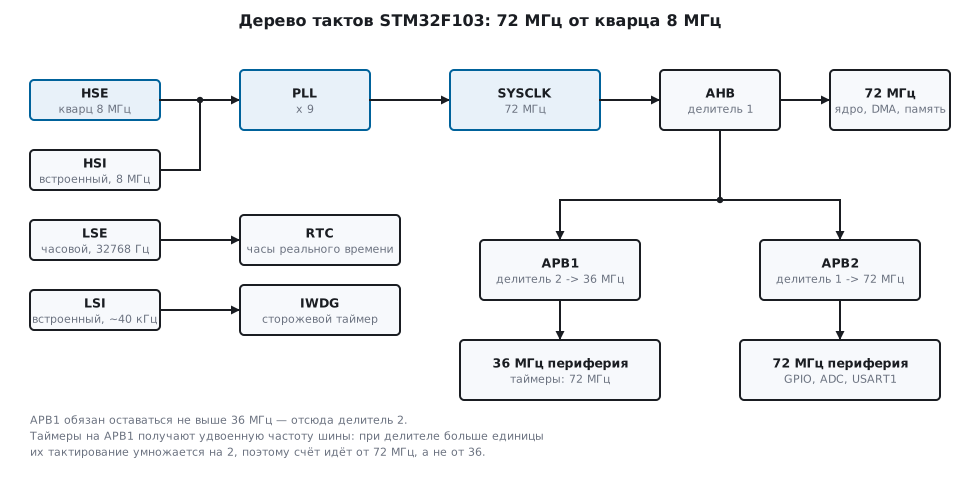
It reads from left to right: an 8 MHz crystal → the PLL multiplies by 9 → 72 MHz becomes
the system frequency → the AHB divider (1 here) gives HCLK for the core, memory and DMA →
then two dividers for the peripheral buses.
Limits that must not be violated (F1):
| Bus | Limit | In the 72 MHz configuration |
|---|---|---|
| SYSCLK, HCLK | 72 MHz | 72 MHz |
| APB2 | 72 MHz | 72 MHz, divider 1 |
| APB1 | 36 MHz | 36 MHz, divider 2 |
| ADC | 14 MHz | divider 6 from APB2 |
The timer trick. Timers get twice the frequency of their APB bus if its divider is greater than one. That is, with APB1 = 36 MHz the timers on it count from 72 MHz, not from 36; APB2 on F1 runs without a divider, and there is no doubling there. This is not an error in the documentation but a feature of the clock routing — yet it regularly breaks the period calculation for those who do not know about it (more in section 13).
6.3 Setting up 72 MHz by hand
The order of steps matters: first the crystal, then the Flash wait states, then the dividers, and only at the very end — switching the system to the PLL.
#define HSE_TIMEOUT  0x5000u

uint8_t SystemClock_72MHz(void)
{
    uint32_t timeout = HSE_TIMEOUT;

    /* 1. Запускаем кварц и ждём готовности — обязательно с таймаутом. */
    RCC->CR |= RCC_CR_HSEON;
    while (!(RCC->CR & RCC_CR_HSERDY)) {
        if (--timeout == 0u) {
            return 1u;                 /* кварц не завёлся */
        }
    }

    /* 2. Flash не успевает за ядром: предвыборка и два такта ожидания. */
    FLASH->ACR |= FLASH_ACR_PRFTBE;
    FLASH->ACR = (FLASH->ACR & ~FLASH_ACR_LATENCY) | 2u;   /* LATENCY = 010: два такта */

    /* 3. Делители шин: AHB = 72, APB2 = 72, APB1 = 36. */
    RCC->CFGR &= ~(RCC_CFGR_HPRE | RCC_CFGR_PPRE1 | RCC_CFGR_PPRE2);
    RCC->CFGR |= RCC_CFGR_HPRE_DIV1;
    RCC->CFGR |= RCC_CFGR_PPRE2_DIV1;
    RCC->CFGR |= RCC_CFGR_PPRE1_DIV2;

    /* 4. PLL: источник HSE, множитель 9. */
    RCC->CFGR &= ~(RCC_CFGR_PLLSRC | RCC_CFGR_PLLXTPRE | RCC_CFGR_PLLMULL);
    RCC->CFGR |= RCC_CFGR_PLLSRC_HSE;
    RCC->CFGR |= RCC_CFGR_PLLMULL9;

    /* 5. Запускаем PLL и ждём захвата. */
    RCC->CR |= RCC_CR_PLLON;
    timeout = HSE_TIMEOUT;
    while (!(RCC->CR & RCC_CR_PLLRDY)) {
        if (--timeout == 0u) {
            return 1u;
        }
    }

    /* 6. Переключаемся и убеждаемся, что переключение состоялось. */
    RCC->CFGR &= ~RCC_CFGR_SW;
    RCC->CFGR |= RCC_CFGR_SW_PLL;
    while ((RCC->CFGR & RCC_CFGR_SWS) != RCC_CFGR_SWS_PLL) {
    }

    return 0u;
}
Three things worth noticing.
A timeout while waiting for the crystal. Most examples simply write
while (!(RCC->CR & RCC_CR_HSERDY)) {}. If the crystal is not soldered, is damaged or
the board is defective — the program will hang here forever, without any sign of life.
Returning an error code lets you fall back to HSI and at least blink an LED.
SW and SWS are different fields. In SW you write the desired source,
and the hardware fills in SWS itself, confirming the actual one. It is
SWS that must be checked: several cycles pass between the write and the switch, and if the PLL
has not locked, the system stays on the previous source.
The multiplier is encoded with an offset. RCC_CFGR_PLLMULL9 is the value 7
in the PLLMUL field, because the encoding is "multiplier minus two". So
do not try to write a nine there.
⚠️ One name — different numbers. In the Keil pack header
stm32f10x.hFLASH_ACR_LATENCY_2equals 2 — "two wait states". In the Cube headerstm32f103xb.h(it is included bystm32f1xx.hin CubeIDE and HAL projects) the same name is bit 2, that is 4: the field gets100, and there is no such value in the register description. Two wait states there isFLASH_ACR_LATENCY_1, in HAL —FLASH_LATENCY_2. That is why in the listing the field is written as a number: the line is correct with both headers.
6.4 Flash wait states — why they are mandatory
Flash memory is slower than the core. At 72 MHz a single instruction fetch does not fit into one cycle, and the Flash controller has to insert wait states.
| Core frequency (F1) | Wait states |
|---|---|
| up to 24 MHz | 0 |
| 24–48 MHz | 1 |
| 48–72 MHz | 2 |
⚠️ The order is critical. Wait states are set before raising the frequency. If you first switch to 72 MHz and then configure
FLASH->ACR, the processor will start reading instructions faster than Flash delivers them, and will get corrupted words. After that anything can happen: wrong numbers, a jump to the wrong place, HardFault. It also happens that at room temperature everything seems to work, but it fails when heated. The reverse order (first lower the frequency, then reduce the wait states) also matters when lowering the frequency.
Prefetch (PRFTBE) reads Flash ahead and partly compensates for the
wait states — it is always worth enabling.
6.5 Peripheral clocks
A separate and the most frequent beginner's mistake: configure a peripheral but forget to supply a clock to it. The register will not be written, and the compiler will say nothing.
RCC->APB2ENR |= RCC_APB2ENR_IOPCEN;    /* порт C */
RCC->APB2ENR |= RCC_APB2ENR_ADC1EN;    /* АЦП 1  */
RCC->APB1ENR |= RCC_APB1ENR_TIM2EN;    /* таймер 2 */
What is on which bus on F1:
| Bus | What is on it |
|---|---|
| AHB | DMA, SRAM, Flash, CRC |
| APB2 (72 MHz) | GPIO, AFIO, ADC1/2/3, USART1, SPI1, TIM1, TIM8 |
| APB1 (36 MHz) | USART2/3, SPI2/3, I2C1/2, TIM2…TIM7, CAN, USB, PWR, DAC |
The practical consequence: USART1 is clocked twice as fast as
USART2, and with the same divider settings it gives a different baud rate.
The BRR register is calculated from the frequency of its own bus.
⚠️ After enabling a peripheral clock, do at least one "idle" operation before writing to its registers. At high frequencies several cycles pass between the write to
APBxENRand the peripheral being ready; ST libraries insert a read-back of the register for this. In practice the problem occurs rarely, but it is agonising to diagnose.
6.6 The same on F4: 168 MHz
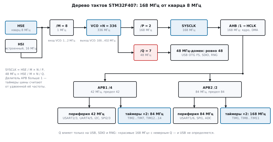
On F4 the tree is more complex: the PLL got three dividers instead of a single multiplier.
SYSCLK = HSE / M × N / P частота USB = HSE / M × N / Q
For 168 MHz from an 8 MHz crystal: M = 8, N = 336, P = 2, Q = 7.
8 МГц / 8   = 1 МГц      ← вход VCO, допустимо 1…2 МГц
1 МГц × 336 = 336 МГц    ← выход VCO, допустимо 100…432 МГц
336 / 2     = 168 МГц    ← системная частота
336 / 7     = 48 МГц     ← ровно то, что требует USB
#define PLL_M   8u
#define PLL_N   336u
#define PLL_P   2u
#define PLL_Q   7u

/* Кварц: запускаем и ждём готовности (с таймаутом, как в 6.3). */
RCC->CR |= RCC_CR_HSEON;
while (!(RCC->CR & RCC_CR_HSERDY)) { }

/* Питание ядра: для 168 МГц нужен режим регулятора Scale 1. */
RCC->APB1ENR |= RCC_APB1ENR_PWREN;
PWR->CR |= PWR_CR_VOS;

/* Делители шин: APB1 не выше 42 МГц, APB2 не выше 84 МГц. */
RCC->CFGR &= ~(RCC_CFGR_HPRE | RCC_CFGR_PPRE1 | RCC_CFGR_PPRE2);
RCC->CFGR |= RCC_CFGR_HPRE_DIV1;
RCC->CFGR |= RCC_CFGR_PPRE1_DIV4;
RCC->CFGR |= RCC_CFGR_PPRE2_DIV2;

/* PLLCFGR собирается целиком: поле P кодируется как (P/2 − 1). */
RCC->PLLCFGR = PLL_M
             | (PLL_N << RCC_PLLCFGR_PLLN_Pos)
             | (((PLL_P >> 1u) - 1u) << RCC_PLLCFGR_PLLP_Pos)
             | (PLL_Q << RCC_PLLCFGR_PLLQ_Pos)
             | RCC_PLLCFGR_PLLSRC_HSE;

/* Flash: 5 тактов ожидания на 168 МГц при 3,3 В, плюс кэши команд и данных. */
FLASH->ACR = FLASH_ACR_ICEN | FLASH_ACR_DCEN | FLASH_ACR_PRFTEN
           | FLASH_ACR_LATENCY_5WS;

/* PLL: запускаем, ждём захвата, переключаемся и проверяем SWS. */
RCC->CR |= RCC_CR_PLLON;
while (!(RCC->CR & RCC_CR_PLLRDY)) { }
RCC->CFGR = (RCC->CFGR & ~RCC_CFGR_SW) | RCC_CFGR_SW_PLL;
while ((RCC->CFGR & RCC_CFGR_SWS) != RCC_CFGR_SWS_PLL) { }
How it differs from F1:
| F1 | F4 | |
|---|---|---|
| PLL | one multiplier ×2…×16 | dividers M, N, P, Q |
| bus limits | APB1 36, APB2 72 | APB1 42, APB2 84 |
| Flash latency at maximum | 2 wait states | 5 wait states |
| Flash cache | prefetch only | instruction and data caches |
| power mode | none | Scale 1 required through PWR->CR |
| HSI frequency | 8 MHz | 16 MHz |
⚠️
Qis the one forgotten most often. It affects only USB, SDIO and the random number generator. You assembled the tree "by eye", got a beautiful 168 MHz — and then spend a week looking for why the USB device is not recognised by the computer. USB requires exactly 48 MHz: withN = 336,Q = 7fits; with otherNthere may be no integer divider at all.⚠️ Keep the VCO input close to 2 MHz. Formally 1…2 MHz is allowed, but the lower the input frequency, the higher the PLL's own noise. ST recommends 2 MHz, so for an 8 MHz crystal
M = 4,N = 168,P = 2,Q = 7is better: at the VCO input 2 MHz, at the output the same 336 MHz, and therefore the same 168 and 48 MHz.
6.7 F0 and G0: clocking
The junior series have a simpler tree than F4, and both can run at full frequency from the internal oscillator — a crystal is needed only for accuracy:
| F1 | F0 | G0 | |
|---|---|---|---|
| internal HSI | 8 MHz | 8 MHz | 16 MHz |
| frequency limit | 72 MHz | 48 MHz | 64 MHz |
| PLL | multiplier | multiplier ×2…×16 | dividers M, N, R, as on G4 and L4 |
| APB buses | two | one | one |
| Flash wait states at maximum | 2 | 1 | 2 |
The HSI frequencies come from the LL headers: HSI_VALUE = 8 MHz on F0 and 16 MHz on G0.
F0: 48 MHz without a crystal. HSI is divided by 2 and multiplied by 12. The multiplier
is encoded with an offset of two, as on F1: RCC_CFGR_PLLMUL12 is 10 in the
PLLMUL field. The Flash latency field is a single bit: 0 or 1 wait state, and one is needed already above
24 MHz:
FLASH->ACR = FLASH_ACR_PRFTBE | FLASH_ACR_LATENCY;   /* выше 24 МГц — один такт ожидания */
RCC->CFGR = (RCC->CFGR & ~(RCC_CFGR_PLLSRC | RCC_CFGR_PLLMUL | RCC_CFGR_PPRE))
          | RCC_CFGR_PLLSRC_HSI_DIV2 | RCC_CFGR_PLLMUL12;
RCC->CR |= RCC_CR_PLLON;
RCC->CFGR = (RCC->CFGR & ~RCC_CFGR_SW) | RCC_CFGR_SW_PLL;
F072 also has HSI48 — a separate 48 MHz oscillator for USB, which is
enabled by the HSI48ON bit in RCC->CR2. By itself it is not accurate enough for USB:
the factory calibration holds −2.8…+2.9 % at 25 °C and −4.9…+4.7 % over the whole
temperature range, while USB Full Speed requires ±0.25 % (section 20).
The accuracy comes from the CRS block: it trims HSI48 by the SOF packets that the host
sends once a millisecond. After reset the CRS synchronisation source is already
USB SOF, and HSI48 is already selected as the USB clock (the USBSW bit in RCC->CFGR3 is 0),
so it remains to enable the block clock (RCC_APB1ENR_CRSEN) and the bits
CRS_CR_AUTOTRIMEN and CRS_CR_CEN. Then USB works without a crystal.
G0: 64 MHz from HSI16. The PLL here is divider M, multiplier N and divider R
at the system clock output. We take the limits from the LL library
(stm32g0xx_ll_utils.c): VCO input 4…8 MHz, the VCO itself 64…344 MHz, the system no higher than
64 MHz. HSI16 / 2 = 8 MHz, × 16 = 128 MHz, / 2 = 64 MHz:
RCC->PLLCFGR = RCC_PLLCFGR_PLLSRC_HSI
             | ((PLL_M - 1u) << RCC_PLLCFGR_PLLM_Pos)    /* M и R — «минус один» */
             | (PLL_N << RCC_PLLCFGR_PLLN_Pos)
             | ((PLL_R - 1u) << RCC_PLLCFGR_PLLR_Pos)
             | RCC_PLLCFGR_PLLREN;                     /* выход R разрешается отдельно */
The register receives 0x30001012 — this can be seen in the object file. Two traps:
M and R are encoded "minus one", while N is as is; the R output without the PLLREN bit
is silent, and switching to the PLL will not work. The Flash latency — two wait states at
64 MHz — is set first, and you wait until it takes effect:
FLASH->ACR = (FLASH->ACR & ~FLASH_ACR_LATENCY) | FLASH_ACR_LATENCY_1 | FLASH_ACR_PRFTEN;
while ((FLASH->ACR & FLASH_ACR_LATENCY) != FLASH_ACR_LATENCY_1) {
}
The system clock source on G0 is a three-bit field: PLL is 010
(RCC_CFGR_SW_1), and the confirmation is read in SWS, as on F1 and F4.
6.8 Trimming HSI
The internal oscillator is an RC network on the die, and its frequency depends on temperature and on the batch. Hence the stated percentages: for blinking an LED it does not matter, for UART at 115200 baud it is already noticeable (section 16: a mismatch of more than 2–3 % breaks reception). But HSI has a trim, and few people use it.
Two fields in RCC->CR are allotted to it:
| Field | Bits | Who writes it |
|---|---|---|
HSICAL |
15:8 | read-only: the factory calibration, loaded at reset |
HSITRIM |
7:3 | your five bits, they are added to the factory ones |
The factory value gets into HSICAL by itself, and HSITRIM after reset always
equals the middle of the range — 16 out of 31. By shifting it, the frequency is moved up or
down relative to the factory value.
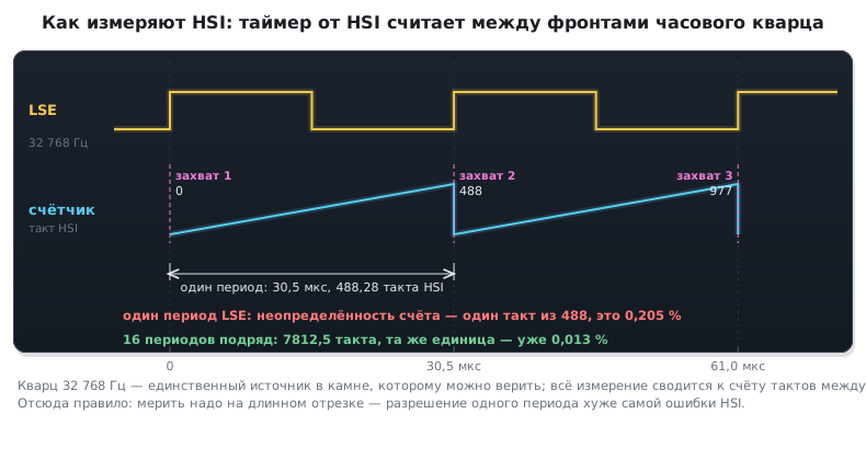
What to compare against. Inside the chip there is one source that can be trusted —
the 32 768 Hz LSE watch crystal. It is routed to a timer's capture input inside
the chip: on F4 this is the TIM5_CH4 input, field TI4_RMP in TIM5->OR = 10 (01 — LSI,
11 — RTC wake-up); on L4 — TIM15 and TIM16 through TIMx->OR1, on G0 —
TIM16 through TIMx->TISEL. F1 has no such path: the CCO bit in BKP->RTCCR
outputs the RTC clock divided by 64 to the TAMPER pin (PC13), and it is connected with a
wire to the capture input. A timer clocked from HSI counts between two
LSE edges; the count is the number of HSI cycles that fit into one period of the
watch crystal. At 16 MHz this is 488.28 cycles. The counting uncertainty is one
cycle, that is 0.205 % per LSE period: worse than the HSI error itself, so measuring
this way is pointless. You have to count over a long interval: over 16 LSE periods
7812.5 cycles accumulate, and the same single cycle of uncertainty now gives
0.013 %.
/* измерение: таймер от HSI считает между фронтами LSE, счёт за 16 периодов */
uint32_t ticks = capture_over(16);              /* захват 16 периодов LSE */
int32_t  want  = 16 * 16000000 / 32768;         /* сколько должно быть: 7812 */
int32_t  err   = (int32_t)ticks - want;         /* знак ошибки: быстрее или медленнее */
Then HSITRIM is moved by one step, the measurement is repeated, and you see in which direction
and by how much the frequency has moved: the step size differs between chips, and it is found by the same
measurement, not out of your head.
⚠️
HSITRIMlives until reset. After a restart the field is 16 again, and if the value found is not saved anywhere, the trim is lost. It is stored in backup registers or in Flash memory and restored at start-up — together with a check that the LSE crystal has started at all.⚠️ Trimming does not turn an RC network into a crystal. It removes the constant offset "this batch is faster", but not the drift with heating: the measurement is valid for the temperature at which it was made. USB and precise interfaces still need HSE — or, on F072, HSI48 trimmed by the CRS block (6.7).
6.9 Pitfalls
A crystal of the wrong frequency. The board has an 8 MHz crystal, but the project specifies
25 MHz (the default on F4) — all calculations are off by a factor of three.
The symptom: HAL_Delay(1000) does not measure a second. The cure is defining
HSE_VALUE in the project settings (see section 2).
Endless waiting for ready. Without a timeout the program hangs on the very first
while (!(RCC->CR & RCC_CR_HSERDY)) loop. The board looks dead, although
the problem is only the crystal.
A forgotten peripheral clock. The most frequent cause of "the code is right but does not work". Register writes silently go nowhere.
Checking SW instead of SWS. The code looks working, but in fact the system
may stay on HSI, and everything will run nine times slower than expected.
Clock security system (CSS). RCC has a mechanism that, when HSE is lost,
automatically switches the system to HSI and raises a non-maskable interrupt.
For products where stopping is unacceptable it is enabled with the RCC_CR_CSSON bit —
but then you need to write an NMI_Handler, otherwise the chip will go
into the default endless loop. The handler clears the flag by writing
RCC->CIR |= RCC_CIR_CSSC (otherwise the NMI will be called again and again) and
reconfigures the clocks: after the event HSE and the PLL are off, and the system runs from HSI.
Clock output (MCO). Any internal frequency can be output on PA8 —
it is convenient to check with an oscilloscope that the PLL really is configured as intended,
instead of guessing from the LED blinking.
6.10 Summary
- After reset the chip runs from the internal RC oscillator: 8 MHz on F1, 16 MHz on F4. Everything else must be configured.
- The configuration order: crystal → Flash wait states → bus dividers → PLL → switch. Flash wait states before raising the frequency, otherwise HardFault.
- On F1 APB1 is no higher than 36 MHz, on F4 no higher than 42. Hence the dividers.
- Timers get twice the frequency of their APB bus (APB1 or APB2) if its divider is greater than 1.
- Always wait for ready with a timeout, and read the switch confirmation
from
SWS, not fromSW. - On F4 the PLL is described by the four M, N, P, Q;
Qis responsible for 48 MHz for USB, and it is forgotten most often. - A peripheral does not work without its clock enabled in
RCC->APBxENR— and does not report this in any way.
Full sources
rcc_f0.c — 48 MHz on STM32F072 from HSI without a crystal.
/* Раздел 6.7: 48 МГц на STM32F072 от внутреннего HSI — без кварца.
 * HSI 8 МГц делится на 2 и умножается PLL на 12. Шина APB у F0 одна. */
#include "stm32f0xx.h"

#define HSI_HZ 8000000u                                /* HSI_VALUE в stm32f0xx_ll_rcc.h */
#define PLL_MUL 12u
#define SYSCLK_HZ (HSI_HZ / 2u * PLL_MUL)

_Static_assert(SYSCLK_HZ == 48000000u, "48 МГц — предел F0");
_Static_assert(RCC_CFGR_PLLMUL12 == ((PLL_MUL - 2u) << RCC_CFGR_PLLMUL_Pos), "множитель со сдвигом на два, как у F1");
_Static_assert(FLASH_ACR_LATENCY == 1u, "у F0 поле задержки — один бит: 0 или 1 такт");

int clock_48mhz_f0(void)
{
    FLASH->ACR = FLASH_ACR_PRFTBE | FLASH_ACR_LATENCY;   /* выше 24 МГц — один такт ожидания */
    RCC->CFGR = (RCC->CFGR & ~(RCC_CFGR_PLLSRC | RCC_CFGR_PLLMUL | RCC_CFGR_PPRE))
              | RCC_CFGR_PLLSRC_HSI_DIV2 | RCC_CFGR_PLLMUL12;
    RCC->CR |= RCC_CR_PLLON;
    for (uint32_t t = 0x5000u; !(RCC->CR & RCC_CR_PLLRDY); t--) {
        if (t == 0u)
            return -1;
    }
    RCC->CFGR = (RCC->CFGR & ~RCC_CFGR_SW) | RCC_CFGR_SW_PLL;
    while ((RCC->CFGR & RCC_CFGR_SWS) != RCC_CFGR_SWS_PLL) {
    }
    return 0;
}

/* F072: HSI48 — отдельный генератор на 48 МГц для USB, кварц не нужен. */
void usb_clock_hsi48_f0(void)
{
    RCC->CR2 |= RCC_CR2_HSI48ON;
    while (!(RCC->CR2 & RCC_CR2_HSI48RDY)) {
    }
}
rcc_g0.c — 64 MHz on STM32G071 from HSI16.
/* Раздел 6.7: 64 МГц на STM32G071 от внутреннего HSI16.
 * PLL устроен как у G4 и L4: делитель M, множитель N, делитель R. */
#include "stm32g0xx.h"

#define HSI_HZ 16000000u                               /* HSI_VALUE в stm32g0xx_ll_rcc.h */
#define PLL_M 2u
#define PLL_N 16u
#define PLL_R 2u
#define VCO_IN_HZ (HSI_HZ / PLL_M)
#define VCO_HZ (VCO_IN_HZ * PLL_N)
#define SYSCLK_HZ (VCO_HZ / PLL_R)

_Static_assert(VCO_IN_HZ >= 4000000u && VCO_IN_HZ <= 8000000u, "вход VCO 4…8 МГц — пределы из stm32g0xx_ll_utils.c");
_Static_assert(VCO_HZ >= 64000000u && VCO_HZ <= 344000000u, "VCO 64…344 МГц");
_Static_assert(SYSCLK_HZ == 64000000u, "64 МГц — предел G0");
_Static_assert(RCC_CFGR_SW_1 == 2u && RCC_CFGR_SWS_1 == 0x10u, "SW = 010 — PLLRCLK");

int clock_64mhz_g0(void)
{
    /* при 64 МГц — два такта ожидания; дождаться, пока задержка вступит в силу */
    FLASH->ACR = (FLASH->ACR & ~FLASH_ACR_LATENCY) | FLASH_ACR_LATENCY_1 | FLASH_ACR_PRFTEN;
    while ((FLASH->ACR & FLASH_ACR_LATENCY) != FLASH_ACR_LATENCY_1) {
    }
    RCC->PLLCFGR = RCC_PLLCFGR_PLLSRC_HSI
                 | ((PLL_M - 1u) << RCC_PLLCFGR_PLLM_Pos)    /* M и R — «минус один» */
                 | (PLL_N << RCC_PLLCFGR_PLLN_Pos)
                 | ((PLL_R - 1u) << RCC_PLLCFGR_PLLR_Pos)
                 | RCC_PLLCFGR_PLLREN;                     /* выход R разрешается отдельно */
    RCC->CR |= RCC_CR_PLLON;
    for (uint32_t t = 0x5000u; !(RCC->CR & RCC_CR_PLLRDY); t--) {
        if (t == 0u)
            return -1;
    }
    RCC->CFGR = (RCC->CFGR & ~RCC_CFGR_SW) | RCC_CFGR_SW_1;
    while ((RCC->CFGR & RCC_CFGR_SWS) != RCC_CFGR_SWS_1) {
    }
    return 0;
}

uint32_t pllcfgr_64mhz(void)
{
    return RCC_PLLCFGR_PLLSRC_HSI | ((PLL_M - 1u) << RCC_PLLCFGR_PLLM_Pos) | (PLL_N << RCC_PLLCFGR_PLLN_Pos)
         | ((PLL_R - 1u) << RCC_PLLCFGR_PLLR_Pos) | RCC_PLLCFGR_PLLREN;
}
Next: section 7 "Interrupts and exceptions" — NVIC, priorities, EXTI and handling the same button without polling in a loop.