 Embedded HandbookApps
38. Consolidated project catalog
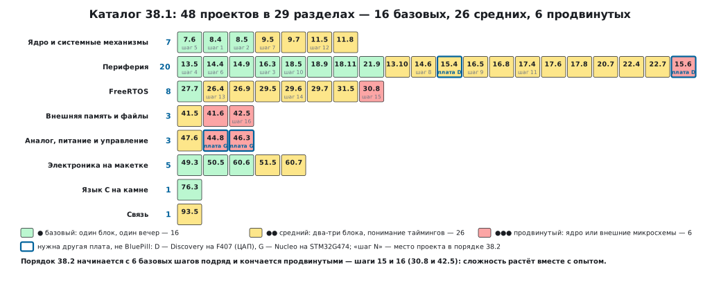
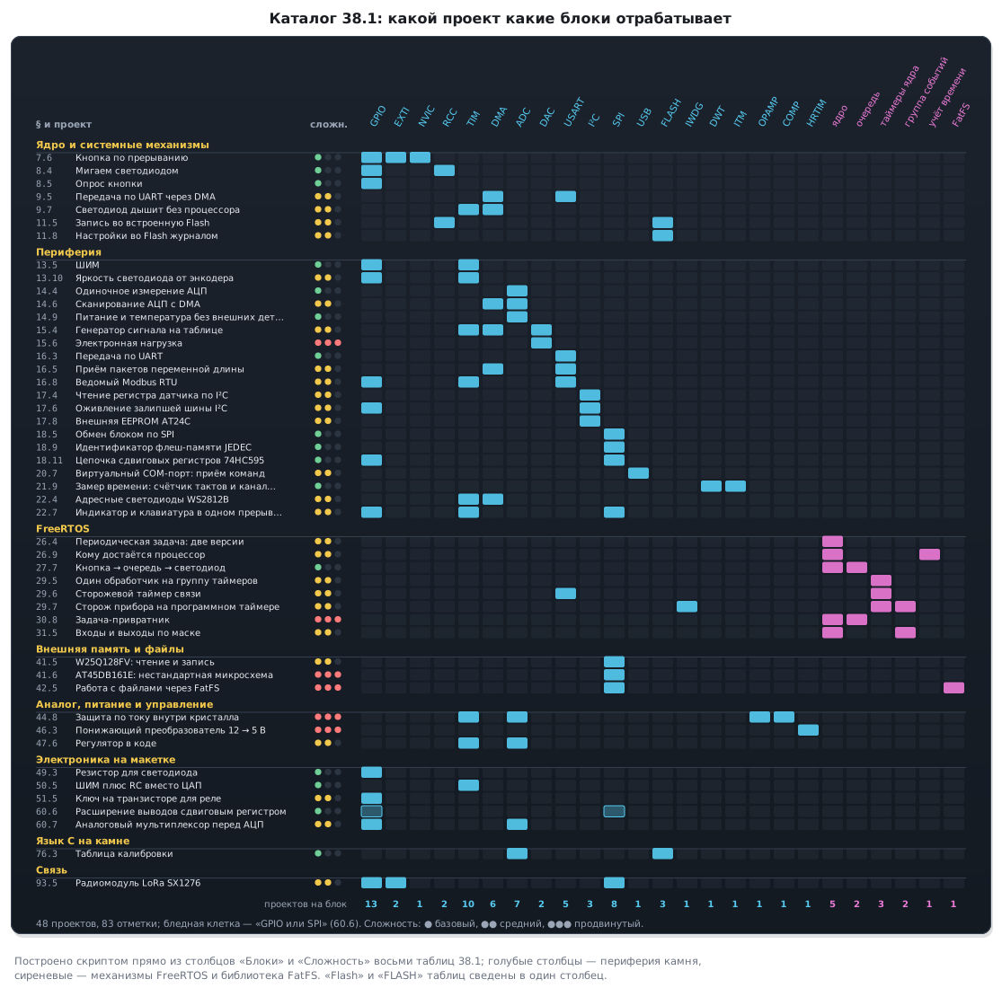
Everything in the handbook marked with the 🔧 icon, in one list. Each item is a finished thing: you can build it on a breadboard, flash it and see the result. For each one you will find what you need beyond the board, which peripherals are involved, how hard it is and what you will understand by doing it. The order follows the sections; the recommended sequence for a beginner is in 38.2.
Legend
● basic: one block, one evening ●● intermediate: two or three blocks, an understanding of timing ●●● advanced: the kernel or external chips, debugging is a must B BluePill, STM32F103C8 D Discovery with the STM32F407: LEDs PD12…PD15, has a DAC; the Nucleo-F401 has its LED onPA5and no DACG Nucleo with the STM32G474 — for the analog blocks and HRTIM Terms used in the documentation
Term Meaning debug probe a debug adapter (ST-Link, J-Link) logic analyzer a logic analyzer operational amplifier (op-amp, OPAMP) an operational amplifier shunt resistor a shunt, a low-value resistor in the current path shift register a shift register multiplexer (mux) a multiplexer, a "selector switch" EEPROM electrically erasable read-only memory flyback / freewheeling diode a suppression (reverse) diode
38.1 Catalog
The core and system mechanisms
| § | Project | Hardware beyond the board | Blocks | Difficulty | What you will understand |
|---|---|---|---|---|---|
| 7.6 | A button on an interrupt | a button, a resistor | EXTI, NVIC, GPIO | ● | the "peripheral → EXTI → NVIC" chain, clearing the flag, bounce |
| 8.4 | Blinking an LED | nothing: PC13 on B, PD12 on D |
GPIO, RCC | ● | the port clock, the CRL/MODER registers, BSRR versus ODR |
| 8.5 | Polling a button | a button | GPIO | ● | pull-up, the active level, debouncing by time |
| 9.5 | UART transmission through DMA | a USB–UART adapter | DMA, USART | ●● | the buffer, DMAT, the difference between "handed over" and "sent out" |
| 9.7 | An LED breathes without the processor | an LED with a resistor on B; not needed on D — PD12 |
TIM, DMA | ●● | DMA writes to a register of another timer, the pace comes from a second timer, circular mode, working in sleep |
| 11.5 | Writing to the internal Flash | nothing | FLASH, RCC | ●● | unlocking, erasing a page, writing by half-words, where to store settings |
| 11.8 | Settings in Flash as a log | nothing; a "save" button if you like | FLASH | ●● | writing records in a row without needless erases, a sequence number and CRC-32, surviving a power loss, the layout version |
Peripherals
| § | Project | Hardware beyond the board | Blocks | Difficulty | What you will understand |
|---|---|---|---|---|---|
| 13.5 | PWM | an LED or a servo | TIM, GPIO | ● | PSC/ARR/CCR, the doubling on APB1, MOE on TIM1 |
| 13.10 | LED brightness from an encoder | a mechanical encoder, an LED with a resistor | TIM, GPIO | ●● | encoder mode ×4, the input filter, the difference of readings across zero, a gamma-corrected scale |
| 14.4 | A single ADC measurement | a potentiometer | ADC | ● | sampling time, calibration on the F1, the pin's analog mode |
| 14.6 | ADC scanning with DMA | two or three sensors | ADC, DMA | ●● | scan mode, a ring buffer, volatile on DMA data |
| 14.9 | Supply voltage and temperature without external parts | nothing | ADC | ● | VREFINT, the factory codes of the F4, integer conversion, the longest sampling time |
| 15.4 | A table-driven signal generator | D (the BluePill and the F401 have no DAC); an oscilloscope or an earphone with a resistor | DAC, DMA, TIM | ●● | a table of samples, triggering by a timer, frequency = clock / (points × period) |
| 15.6 | An electronic load | D (the BluePill and the F401 have no DAC); an op-amp, a MOSFET on a heatsink, a 1 Ω shunt | DAC | ●●● | the DAC sets the current through the op-amp loop, the DAC buffer is off, the power heats the transistor |
| 16.3 | UART transmission | a USB–UART adapter | USART | ● | TXE versus TC, the baud rate divider, a terminal |
| 16.5 | Receiving variable-length packets | a USB–UART adapter | USART, DMA | ●● | detecting the IDLE gap, a ring buffer, ORE |
| 16.8 | A Modbus RTU slave | a USB–UART adapter or an RS-485 transceiver; the master on a computer | USART, TIM, GPIO | ●● | an 11-bit character, end of frame by a 3.5-character gap, exceptions, the transmitter by TC |
| 17.4 | Reading a sensor register over I²C | any sensor with I²C | I²C | ●● | start — address — register — restart — read; ADDR and both SR |
| 17.6 | Reviving a stuck I²C bus | a sensor with I²C | I²C, GPIO | ●● | nine clocks by hand, why the slave holds SDA |
| 17.8 | An external AT24C EEPROM | a 24C04 or 24C08 chip | I²C | ●● | page writes, polling for readiness, the upper bits of the cell address in the device address |
| 18.5 | Exchanging a block over SPI | any chip with SPI | SPI | ● | CPOL/CPHA, BSY before releasing CS, full duplex |
| 18.9 | The JEDEC flash memory identifier | an SPI Flash chip | SPI | ● | command 0x9F, skipping the first response, 0xFF and 0x00 as signs of a broken connection |
| 18.11 | A chain of 74HC595 shift registers | two or three 74HC595 chips, LEDs | SPI, GPIO | ● | the byte order in the chain, latching after BSY |
| 20.7 | Virtual COM port: receiving commands | a USB cable; on B — a 1.5 kΩ pull-up on D+ | USB | ●● | a packet is not a string, a ring between the interrupt and the loop, character-by-character input, USBD_BUSY when transmitting |
| 21.9 | Measuring time: the cycle counter and an ITM channel | a debugger that receives SWO | DWT, ITM | ● | CYCCNT, a separate channel for numbers, the 0x0B packet and a word |
| 22.4 | WS2812B addressable LEDs | a strip or several LEDs, a 5 V supply | TIM, DMA | ●● | PWM + DMA as a code generator, ±150 ns timing, GRB order |
| 22.7 | Display and keypad in one interrupt | a four-digit display, two 74HC595, a 4×4 keypad, digit transistors | TIM, SPI, GPIO | ●● | multiplexed display at 250 Hz per digit, rows as open-drain, 20 ms debouncing |
FreeRTOS
| § | Project | Hardware beyond the board | Blocks | Difficulty | What you will understand |
|---|---|---|---|---|---|
| 26.4 | A periodic task: two versions | an LED | kernel | ●● | vTaskDelay versus xTaskDelayUntil, period drift in numbers |
| 26.9 | Who gets the CPU | nothing | kernel, run-time accounting | ●● | time slicing, starvation, waiting gives time to lower priorities, priority cut after configASSERT |
| 27.7 | Button → queue → LED | a button, an LED | kernel, queue | ● | the queue timeout as a timer, bounce, sending without waiting and counting losses |
| 29.5 | One handler for a group of timers | three LEDs | kernel timers | ●● | the timer ID, the daemon, zero wait in a callback |
| 29.6 | A link watchdog timer | a USB–UART adapter | kernel timers, USART | ●● | a one-shot timer restarted from an interrupt, FromISR |
| 29.7 | A device watchdog on a software timer | nothing | kernel timers, event group, IWDG | ●● | the daemon is always alive, task check-ins in an event group, read-and-clear in one call |
| 30.8 | The gatekeeper task | a USB–UART adapter | kernel, queue | ●●● | a resource without a mutex, requests from interrupts, no deadlocks |
| 31.5 | Inputs and outputs by mask | four buttons, four LEDs | kernel, event group | ●● | "all" and "any", a change flag instead of waiting for a mask, the rule changes on the fly |
External memory and files
| § | Project | Hardware beyond the board | Blocks | Difficulty | What you will understand |
|---|---|---|---|---|---|
| 41.5 | W25Q128FV: reading and writing | an SPI Flash chip | SPI | ●● | JEDEC ID, Write Enable, erasing before writing, BUSY |
| 41.6 | AT45DB161E: a non-standard chip | a chip with a buffered architecture | SPI | ●●● | how a "different" flash differs: buffers, a page size of 528, reading the status |
| 42.5 | Working with files through FatFS | an SD card or SPI Flash | SPI, FatFS | ●●● | the disk layer, f_mount/f_open/f_write/f_sync, what breaks when power is switched off |
Analog, power and control
| § | Project | Hardware beyond the board | Blocks | Difficulty | What you will understand |
|---|---|---|---|---|---|
| 44.8 | Overcurrent protection inside the chip | G; a 10 mΩ shunt, a switch, a load up to 10 A | OPAMP, COMP, TIM, ADC | ●●● | shunt → amplifier ×16 → comparator → the timer's fault input: PWM shuts off without the program |
| 46.3 | A 12 → 5 V buck converter | G or F334; a half-bridge with a driver, an inductor, a capacitor | HRTIM | ●●● | 54 400 steps per 100 kHz period, a complementary pair with dead time, the fault input |
| 47.6 | A controller in code | a 10 ms RC circuit or a heater with a sensor | TIM, ADC | ●● | a constant period, a limit on the integrator, the derivative on the measurement |
Electronics on a breadboard
| § | Project | Hardware beyond the board | Blocks | Difficulty | What you will understand |
|---|---|---|---|---|---|
| 49.3 | A resistor for an LED | an LED, a resistor | GPIO | ● | the voltage budget: the drop across the pin, the resistor and the LED |
| 50.5 | PWM plus RC instead of a DAC | a 10 kΩ resistor, a 1 µF capacitor | TIM | ● | the average equals the duty cycle, with an 82.5 mV peak-to-peak sawtooth on top at 1 kHz |
| 51.5 | A transistor switch for a relay | a transistor, a 12 V relay, a suppression diode, a 510 Ω resistor, a 12 V supply | GPIO | ●● | a forced gain of 10…20, a base current of 5 mA, why the coil needs a diode |
| 60.6 | Expanding outputs with a shift register | a shift register with a latch, eight LEDs | GPIO or SPI | ● | three pins for any number of outputs, the latch, 4 µs for 32 outputs at 8 MHz |
| 60.7 | An analog multiplexer in front of the ADC | an 8-channel analog multiplexer | ADC, GPIO | ●● | the channel resistance adds to the source: 4.2 µs of sampling for 100 kΩ |
The C language on the chip
| § | Project | Hardware beyond the board | Blocks | Difficulty | What you will understand |
|---|---|---|---|---|---|
| 76.3 | A calibration table | a sensor with a non-linear characteristic | ADC, Flash | ● | a const table in Flash, binary search, integer interpolation |
Communication
| § | Project | Hardware beyond the board | Blocks | Difficulty | What you will understand |
|---|---|---|---|---|---|
| 93.5 | The LoRa SX1276 radio module | an SX1276 module with an antenna; two for a link | SPI, GPIO, EXTI | ●● | radio module registers: the LoRa bit in sleep, the frequency in 64 bits, flags cleared by writing ones |
38.2 Recommended order
For someone starting from scratch on a BluePill — sixteen steps, each building on the previous ones:
| Step | § | Why now |
|---|---|---|
| 1 | 8.4 | the first firmware; make sure the "build → download → board" chain works |
| 2 | 8.5 | the first input and the first bounce |
| 3 | 16.3 | text output to a terminal — without it you have nothing to debug with later |
| 4 | 13.5 | the first timer, the first understanding of frequencies |
| 5 | 7.6 | the first interrupt; compare it with the polling from step 2 |
| 6 | 14.4 | the first measurement; print it to the terminal from step 3 |
| 7 | 9.5 | the first DMA on the already familiar UART |
| 8 | 14.6 | DMA on the ADC: two familiar blocks together |
| 9 | 16.5 | receiving is harder than transmitting; this is where buffers and IDLE appear |
| 10 | 18.5 | SPI is simpler than I²C, an easier way to start with buses |
| 11 | 17.4 | I²C with a real sensor |
| 12 | 11.5 | save the settings you have collected over ten steps |
| 13 | 26.4 | the first task under the kernel — on the already familiar LED |
| 14 | 29.6 | kernel timers on the already familiar UART |
| 15 | 30.8 | the gatekeeper: the kernel in earnest |
| 16 | 42.5 | files on a card — the crowning step: SPI, the kernel, external memory together |
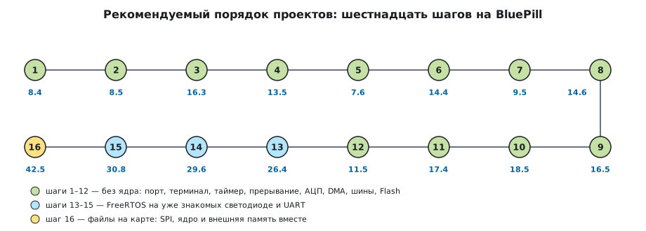
After the sixteenth step the rest of the catalog can be done in any order.
38.3 What you need
A minimal kit that covers the whole catalog:
| What for | |
|---|---|
| BluePill or Nucleo/Discovery | everything; 15.4 and 15.6 only on the Discovery with the F407 (DAC) |
| an ST‑Link debugger (not a clone — if you need SWO) | downloading, debugging, 21.9 |
| a USB–UART adapter | 9.5, 16.x, 29.6, 30.8 |
| an RS-485 transceiver (optional) | 16.8 |
| a breadboard, wires, buttons, LEDs, resistors | 7.6, 8.5, 9.7, 13.5, 26.4, 27.7, 29.5, 49.3 |
| a potentiometer; for scanning — two or three potentiometers or sensors | 14.4, 14.6 |
| a mechanical encoder | 13.10 |
| a USB cable; on the BluePill — a 1.5 kΩ resistor on D+ | 20.7 |
| four buttons and four LEDs | 31.5 |
| an op-amp, a MOSFET on a heatsink, a 1 Ω shunt | 15.6 |
| any sensor with I²C | 17.x |
| a 24C04 or 24C08 EEPROM chip | 17.8 |
| an SPI Flash chip | 18.5, 18.9, 41.x |
| an SD card with an adapter | 42.5 |
| a WS2812B strip and a 5 V supply | 22.4 |
| a four-digit display, a 4×4 keypad, two 74HC595, digit transistors | 22.7 |
| an oscilloscope or a logic analyzer | 15.4, 22.4, and desirable in general |
| a Nucleo board with the STM32G474 | 44.8, 46.3 |
| a 10 mΩ shunt, a switch and a load up to 10 A; a half-bridge with a driver, an inductor, a capacitor | 44.8, 46.3 |
| a transistor, a 12 V relay, a suppression diode, a 12 V supply | 51.5 |
| a shift register, an analog multiplexer, resistors and capacitors | 18.11, 47.6, 50.5, 60.6, 60.7 |
| a sensor with a non-linear characteristic | 76.3 |
| two LoRa modules on the SX1276 with antennas | 93.5 |
The oscilloscope is the only expensive item on the list, and you can do without it almost everywhere. But section 36 ends with the words "an oscilloscope on the line" for a reason: what is on the wire, not what should be there, is the answer to half of the "works sometimes" questions.
38.4 Summary
- The 38.1 catalog is assembled from all subsections marked 🔧 and is checked against them at every release.
- The 38.2 order is sixteen steps from the first LED to files on a card: each builds on the previous ones.
- The 38.3 kit covers the whole catalog; the oscilloscope is the only expensive item and is not always needed.
Next: section 38а "Interview questions: a hundred questions on the handbook with short answers and a section reference".