 Embedded HandbookApps
198к. Mini-project: an oscilloscope on the board — ADC, DMA, edge trigger and a display on the PC
In section 198д the board became a logic analyzer: eight digital inputs, a timer and DMA. Here is its analog sibling: a single-channel oscilloscope on the F407. A timer sets the sampling rate to 1 MSa/s, the ADC writes samples through DMA into a double buffer, the core looks for an edge with hysteresis and assembles a frame of 1024 samples with pre-trigger, decimates the signal at slow time bases, and the frame with a CRC goes over UART to the computer, where a Python program checks it, measures the frequency and draws the picture.
Everything is tested without a board. The oscilloscope core (scope_core.c) does not touch
the hardware, so the same experiment program sim_scope.c is built with gcc on the
PC and with arm-none-eabi-gcc for the Cortex-M4 and run in
qemu-system-arm -M netduinoplus2 (output through semihosting, section 35а):
instead of the ADC, the samples come from a generator with integer arithmetic. The PC output
and the QEMU output matched line for line. The firmware that configures TIM2, ADC1, DMA2 and
USART1 (scope_f407.c) is built with armclang against the F4 pack headers without
warnings; it has not been run on hardware.
Sources: table 67 "ADC characteristics" and equation 1 of datasheet DS8626
(STM32F405/407), RM0090: the EXTSEL trigger selection, the ADCPRE prescaler,
table 43 of DMA2 requests, double buffer mode (10.3.9); DMA is section 9,
timers 13, the ADC 14, the USB CDC ceiling section 198б. The check is
_verify/scope198k_check.py.
Terms used in the documentation
Term Meaning sampling rate samples per second external trigger (EXTSEL, EXTEN) external start of conversion: from what source and on which edge TRGO the timer trigger output for other peripherals double buffer mode (DBM), current target (CT) the DMA double buffer and the "where we are writing now" bit trigger level, hysteresis the trigger threshold and the hysteresis pre-trigger samples recorded before the trigger point auto trigger "auto": a frame on timeout if there is no edge decimation keeping one sample out of D aliasing a high frequency looks like a low one dead time the signal goes on, but the instrument is not looking at it
198к.1 What the instrument does and what it is made of
| Function | How |
|---|---|
| input | PA1 = ADC123_IN1, 0…3.3 V, 12 bits |
| sampling rate | TIM2 84 MHz / 84 = 1 MHz → TRGO → ADC1 start |
| moving the samples | DMA2 Stream0, channel 0, double buffer of 512 samples per half |
| frame | 1024 samples, 256 of them before the trigger |
| trigger | on an edge through a threshold with hysteresis; "auto" on timeout |
| slow time base | decimation by D: the average or every D-th sample |
| link to the PC | a 1550-byte frame with CRC-16, USART1 at 2 Mbaud through DMA2 Stream7 |
| on the PC | scope_host.py: check, unpacking, frequency, peak-to-peak, PNG |
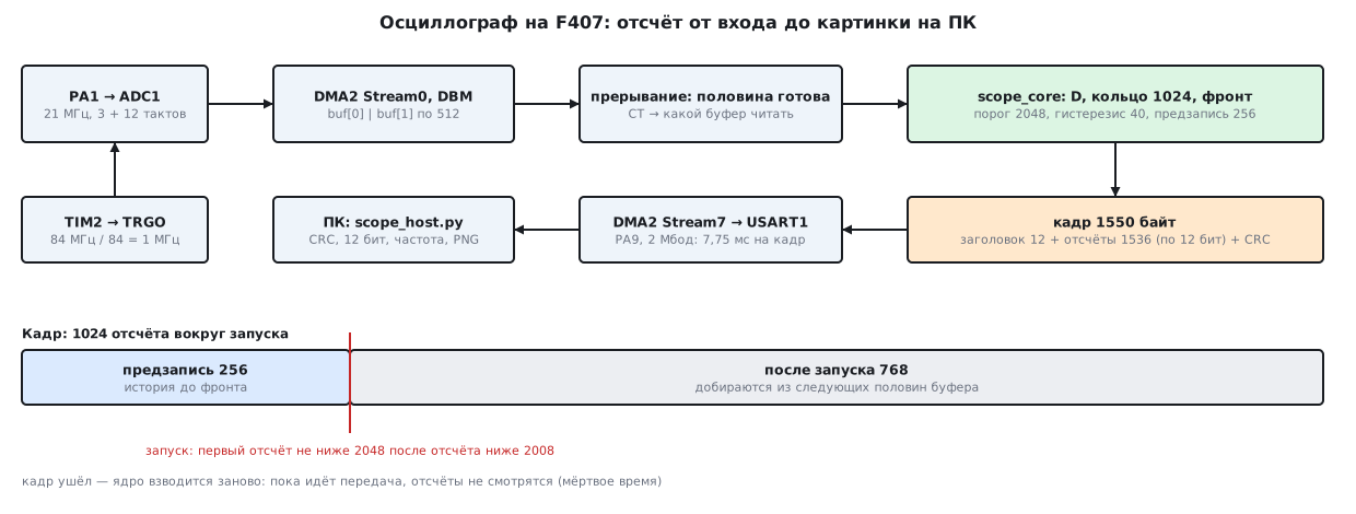
This is an instrument "until you have an instrument", like the analyzer from 198д: the bandwidth is hundreds of kilohertz, there is one channel, there is no probe with a divider and no input protection, so the input is limited to 0…3.3 V. But everything inside is visible: where the sampling rate ceiling comes from, how not to lose the beginning of a signal, and why decimation should use the average rather than throwing samples away.
198к.2 Sampling rate, bandwidth and resolution: working it out from the datasheet
Table 67 of DS8626 gives, for the F407 ADC at a supply of 2.4…3.6 V, a clock
frequency fADC of no more than 36 MHz. The ADC clock is derived from PCLK2 by the
ADCPRE prescaler: 2, 4, 6 or 8. With PCLK2 = 84 MHz:
| Prescaler | fADC |
Usable? |
|---|---|---|
| 2 | 42 MHz | no: above 36 MHz |
| 4 | 21 MHz | yes, chosen |
| 6 | 14 MHz | yes |
| 8 | 10.5 MHz | yes |
A 12-bit conversion is the sampling time plus 12 clock cycles. The shortest
sampling time is 3 cycles, 15 cycles in total: at 21 MHz that is 1.4 MSa/s back to back.
But with a timer trigger you cannot go faster: the same table limits the external trigger to
fADC / 17, that is 1.235 MSa/s. 1 MSa/s is chosen, exactly 84 timer
clocks. For comparison, at fADC = 30 MHz the datasheet gives 2 MSa/s for
one ADC, 3.75 for two interleaved and 6 for three; with
PCLK2 = 84 MHz you cannot get 30 MHz, only 21.
A short sampling time needs a strong source. Equation 1 of DS8626 gives
the largest source resistance at which the error stays below a quarter of an
LSB: RAIN = (k − 0,5) / (fADC · CADC · ln 2^(N+2)) − RADC,
where CADC = 4 pF, RADC = 6 kΩ (table 67). At 21 MHz:
| Sampling, cycles | RAIN at most |
Sampling rate ceiling |
|---|---|---|
| 3 | below zero | 1400 kHz |
| 15 | 11788 Ω | 777.8 kHz |
| 28 | 27736 Ω | 525.0 kHz |
At 3 cycles the equation gives a negative number: a quarter of an LSB is not promised for any source. What remains is a source with the lowest possible resistance, an op-amp follower, with an error above a quarter of an LSB, or a longer sampling time, at the cost of the rate.
Resolution: the LSB with a 3.3 V reference is 0.806 mV; the total
unadjusted error from table 68 (at fADC = 30 MHz) is up to
±5 LSB, that is up to ±4.0 mV. Bandwidth: at 1 MSa/s the Kotelnikov (Nyquist) theorem sets the limit at
500 kHz, but to see a waveform on the screen rather than dots you need at least ten
samples per period, which means 100 kHz.
198к.3 Capture: the timer, the ADC and the DMA double buffer
The chain is configured once. TIM2 overflows once every microsecond and
outputs TRGO; on the TRGO edge (EXTSEL = 0110 per RM0090) the ADC performs
one conversion and asks DMA to pick up the result. ADC1 is served by
DMA2 Stream0, channel 0 (table 43 of RM0090):
    DMA2_Stream0->PAR = (uint32_t)&ADC1->DR;
    DMA2_Stream0->M0AR = (uint32_t)buf[0];
    DMA2_Stream0->M1AR = (uint32_t)buf[1];
    DMA2_Stream0->NDTR = HALF;
    DMA2_Stream0->CR = (0u << DMA_SxCR_CHSEL_Pos)                         /* канал 0 потока 0 — ADC1 */
                     | DMA_SxCR_DBM | DMA_SxCR_PL_1 | DMA_SxCR_MSIZE_0 | DMA_SxCR_PSIZE_0
                     | DMA_SxCR_MINC | DMA_SxCR_TCIE;
In double buffer mode (RM0090, 10.3.9) the stream has two memory addresses, and
at the end of each transfer DMA switches to the other one by itself; circular mode
is enabled automatically. While DMA writes into one half, the processor reads
the other. Which one is told by the CT bit:
void DMA2_Stream0_IRQHandler(void)
{
    DMA2->LIFCR = DMA_LIFCR_CTCIF0;
    const uint16_t *ready = (DMA2_Stream0->CR & DMA_SxCR_CT) ? buf[0] : buf[1];
    if (sc.state == SC_DONE)
        return;                                                           /* кадр ещё не ушёл — мёртвое время */
    sc_feed(&sc, ready, HALF);
    if (sc.state == SC_DONE && !tx_busy)
        send_frame();
}
To process a half, the interrupt has exactly the time it takes to fill the other one: 512 samples at 1 MHz, 512 µs. If it is late, DMA starts overwriting the half that is still being read.
Frequencies and fields are checked at build time: _Static_assert in
scope_f407.c requires fADC ≤ 36 MHz, 3 + 12 cycles per sample, a trigger
no more often than fADC / 17, and the positions of the EXTSEL, EXTEN, ADCPRE,
DBM, CT, CHSEL fields as in RM0090. armclang 6.24 built scope_f407.c and
scope_core.c without warnings: 518 and 716 bytes of code, 5688 bytes of RAM
for the firmware: two buffers of 1024 bytes, a 1550-byte frame and the core state of
2088 bytes.
198к.4 Edge trigger and pre-trigger
An oscilloscope must show not only what happened after the edge but also what happened before it. So the samples are written into a ring all the time, and the trigger only marks the place. The ring holds 1024 samples, exactly one frame: once 1024 − 256 = 768 samples have accumulated after the trigger, the ring holds 256 samples before the edge and 768 after.
    case SC_WAIT:
        if ((int32_t)v < (int32_t)s->level - (int32_t)s->hyst)
            s->armed = 1;               /* сигнал ушёл ниже порога — фронт снова возможен */
        else if (s->armed && v >= s->level) {
            trig(s, SC_F_TRIG);
            break;
        }
        if (s->auto_after && ++s->waited >= s->auto_after)
            trig(s, SC_F_AUTO);
        break;
The state machine waits until the ring has accumulated the pre-trigger, then "arms" when the signal drops below the threshold minus the hysteresis, and fires on the first sample not below the threshold. Experiment 1: a 10 kHz sine with 2000 codes peak-to-peak and noise, threshold 2048, hysteresis 40: the trigger fires on sample 301; in the frame the sample before the edge is 2043, the one on the edge is 2104. The frame is ready after three buffer halves (1536 samples).
Why hysteresis. Experiment 5 is a frequency counter on the same state machine: a 1 kHz sine with heavy noise (the sum of two uniform distributions of ±100 codes), 100 ms, that is, 100 real edges:
| Hysteresis, codes | Edges counted |
|---|---|
| 0 | 1517 |
| 40 | 1137 |
| 200 | 234 |
| 400 | 100 |
Noise on a slope crosses the threshold back and forth many times. What helps is hysteresis larger than the noise peak-to-peak (here ±200, so 400 peak-to-peak), not its amplitude.
"Auto". If there is no edge at all, a real oscilloscope still shows a trace. Experiment 4: a constant 1500 codes, a timeout of 5000 samples: a frame with the "auto" flag, all samples 1500.
198к.5 Decimation: the average against "every D-th"
To fit 10 ms instead of 1 ms into 1024 samples, the rate after the ADC is reduced by a factor of D. There are two ways to do this, and they give different results.
The average of D samples is both decimation and a filter. Experiment 2: the same 10 kHz sine with noise, D = 10. The noise relative to the clean signal:
| Run | Model | |
|---|---|---|
| D = 1 | 10.17 codes | 10.20 (sum of two uniform distributions of ±12) |
| D = 10, average | 3.21 codes | 3.24 (√10 times smaller plus rounding) |
Every D-th sample gives no filtering, and everything above half the new sampling rate folds back into the band. Experiment 3: a 97 kHz sine, D = 10, a new rate of 100 kHz:
| Method | Peak-to-peak in the frame | What you see |
|---|---|---|
| every tenth | 1999 codes | a false 3000 Hz sine at full amplitude, and the edge was found |
| average of ten | 62 codes | an almost flat line, a frame on "auto" |
A model of the average: the gain at frequency f is |sin(π·f·D/fs) / (D·sin(π·f/fs))|; for 97 kHz it is 0.0314, −30.1 dB, an expected peak-to-peak of 62.7 codes; the run gives 62. "Every tenth" showed a signal that does not exist: 97 kHz looks like 3 kHz. The average does not remove aliasing completely, but it suppresses it by tens of decibels.
198к.6 The frame, the link to the PC and the program on the computer
A frame is a 12-byte header (the A5 5A marker, number, "edge/auto" flags, D,
pre-trigger, number of samples, threshold), the samples and a CRC-16/CCITT. An ADC sample is
12 bits, so two samples are packed into three bytes: 1536 bytes instead of 2048,
a saving of 512 bytes. 1550 bytes in total.
The link: USART1 on PCLK2 = 84 MHz, 2 Mbaud, BRR = 42, with no error.
A byte on the wire is 10 bits, so a frame takes 7.75 ms: no more than 129 frames per
second. The full-speed USB CDC ceiling from section 198б is
1216000 bytes/s; a frame over it takes 1.27 ms. A continuous stream at
1 MSa/s of 1.5 bytes each is 1500000 bytes/s, more than the CDC ceiling. That is why
the instrument sends frames, not a stream: while a frame is being sent, the core does not look at
samples. That is the dead time.
scope_host.py parses the frames from the experiment output:
- all 5 frames are 1550 bytes each, and the CRC matched for all of them;
- our own Python model (the same generator, its own decimation and its own trigger state machine) produced the same samples as the C core in all five frames;
- the frequency from edges with interpolation: experiment 1 gives 10000.9 Hz, experiment 2 10000.0 Hz, experiment 3 "every tenth" 3000.0 Hz; the peak-to-peak of experiment 1 is 1.642 V;
- the picture: matplotlib 3.10.9, PNG 900 × 600: the frame of experiment 1 with the trigger mark and both frames of experiment 3.
198к.7 Pitfalls
The frame "drifts" on a noisy signal. A trigger without hysteresis fires on the noise near the threshold: in the experiment, 1517 edges instead of 100. Make the hysteresis larger than the noise peak-to-peak.
You cannot see what happened before the edge. Recording is started at the trigger, and the beginning is lost. The ring is written all the time, the trigger only marks the place, and the pre-trigger must accumulate before the state machine arms.
The interrupt did not keep up. It has 512 µs per buffer half. If processing takes longer, DMA starts writing into the same half, and samples from different moments end up in the frame. The processing time on the board was not measured here.
DMA buffer in CCM. On the F407 the memory at address 0x1000 0000 is visible only
to the core (RM0090): DMA will not fill a buffer that the linker
placed there.
ADCPRE = 2 "for speed". 84 / 2 = 42 MHz, above the 36 MHz from
table 67: operation outside the datasheet characteristics.
Triggering faster than fADC / 17. At 21 MHz the timer-trigger ceiling is 1.235 MSa/s,
although the ADC manages 1.4 "back to back". Faster is again outside table 67.
3 sampling cycles from a 100 kΩ divider. According to the DS8626 equation, at 3 cycles the allowed source resistance is below zero. You need a follower or a longer sampling time, otherwise the error is larger than the one the equation promises.
Decimation by throwing samples away. A signal above half the new sampling rate is drawn as a false low frequency: 97 kHz as 3 kHz. Decimate with the average (or put an analog filter before the ADC).
"A stream over UART". 1 MSa/s at 12 bits is 1.5 MB/s: more than both 2 Mbaud and the USB CDC ceiling. Only frames, with dead time.
198к.8 Summary
- F407:
fADC= 84 / 4 = 21 MHz (no more than 36), 3 + 12 cycles give 1.4 MSa/s back to back, no more than 1.235 with a timer trigger; 1 MSa/s is chosen. - Bandwidth up to 500 kHz by Kotelnikov (Nyquist), waveform up to 100 kHz (ten samples per period); the LSB is 0.806 mV.
- At 3 sampling cycles the DS8626 equation gives a negative source resistance limit, so a follower is needed; at 15 cycles, up to 11788 Ω.
- A DMA double buffer of 512 samples per half gives 512 µs to process a half.
- A 1024-sample ring: 256 pre-trigger, 768 after the trigger; a hysteresis of 400 codes gave 100 edges out of 100 instead of 1517.
- Average of 10 samples: noise 10.17 → 3.21 codes, 97 kHz attenuated to 62 codes peak-to-peak (−30.1 dB); "every tenth" drew a false 3000 Hz.
- A 1550-byte frame with CRC: 7.75 ms over UART at 2 Mbaud, 1.27 ms over USB CDC; the Python model matched the C core in all 5 frames, frequency 10000.9 Hz.
Full sources
scope_core.c — the oscilloscope core: decimation, history ring, edge trigger.
/* Раздел 198к: ядро осциллографа. Отсчёты приходят блоками (половина двойного буфера DMA),
 * прореживаются, пишутся в кольцо истории; запуск — по фронту через порог с гистерезисом. */
#include "scope_core.h"

void sc_rearm(scope_t *s)
{
    s->wr = 0;
    s->acc = 0;
    s->accn = 0;
    s->state = SC_FILL;
    s->armed = 0;
    s->flags = 0;
    s->trig_at = 0;
    s->waited = 0;
}

void sc_init(scope_t *s, uint16_t level, uint16_t hyst, uint16_t pre, uint16_t decim, uint8_t mode, uint32_t auto_after)
{
    s->level = level;
    s->hyst = hyst;
    s->pre = pre < SC_N ? pre : (uint16_t)(SC_N - 1u);
    s->decim = decim ? decim : 1u;
    s->mode = mode;
    s->auto_after = auto_after;
    sc_rearm(s);
}

static void trig(scope_t *s, uint8_t why)
{
    s->trig_at = s->wr - 1u;            /* отсчёт, на котором сработал запуск */
    s->flags = why;
    s->state = SC_POST;
}

/* Один прореженный отсчёт: в кольцо, затем автомат запуска. */
static void push(scope_t *s, uint16_t v)
{
    s->ring[s->wr % SC_N] = v;
    s->wr++;
    switch (s->state) {
    case SC_FILL:                       /* копим историю: предзапись должна быть полной */
        if (s->wr >= s->pre)
            s->state = SC_WAIT;
        break;
    case SC_WAIT:
        if ((int32_t)v < (int32_t)s->level - (int32_t)s->hyst)
            s->armed = 1;               /* сигнал ушёл ниже порога — фронт снова возможен */
        else if (s->armed && v >= s->level) {
            trig(s, SC_F_TRIG);
            break;
        }
        if (s->auto_after && ++s->waited >= s->auto_after)
            trig(s, SC_F_AUTO);
        break;
    case SC_POST:                       /* добираем кадр после запуска */
        break;
    default:
        return;
    }
    if (s->state == SC_POST && s->wr - s->trig_at >= (uint32_t)SC_N - s->pre)
        s->state = SC_DONE;
}

uint32_t sc_feed(scope_t *s, const uint16_t *x, uint32_t n)
{
    uint32_t i;
    for (i = 0; i < n && s->state != SC_DONE; i++) {
        if (s->mode == SC_SKIP) {       /* каждый D-й: всё выше fs/2D заворачивается в полосу */
            if (s->accn == 0u)
                push(s, x[i]);
            if (++s->accn == s->decim)
                s->accn = 0;
        } else {                        /* среднее D отсчётов: и прореживание, и фильтр */
            s->acc += x[i];
            if (++s->accn == s->decim) {
                push(s, (uint16_t)((s->acc + s->decim / 2u) / s->decim));
                s->acc = 0;
                s->accn = 0;
            }
        }
    }
    return i;                           /* сколько отсчётов блока взято; остаток — мёртвое время */
}

uint16_t sc_sample(const scope_t *s, uint32_t i)
{
    return s->ring[(s->trig_at - s->pre + i) % SC_N];
}

uint16_t sc_crc16(const uint8_t *p, size_t n)
{
    uint16_t c = 0xFFFFu;               /* CRC-16/CCITT-FALSE: 0x1021, начальное 0xFFFF */
    while (n--) {
        c ^= (uint16_t)(*p++ << 8);
        for (int k = 0; k < 8; k++)
            c = (uint16_t)((c & 0x8000u) ? ((uint32_t)c << 1) ^ 0x1021u : (uint32_t)c << 1);
    }
    return c;
}

static uint8_t *le16(uint8_t *p, uint16_t v)
{
    p[0] = (uint8_t)v;
    p[1] = (uint8_t)(v >> 8);
    return p + 2;
}

/* Кадр: A5 5A, номер, флаги, D, предзапись, N, порог; отсчёты по 12 бит — два в трёх байтах; CRC-16. */
size_t sc_encode(const scope_t *s, uint8_t seq, uint8_t *buf)
{
    uint8_t *p = buf;
    *p++ = 0xA5u;
    *p++ = 0x5Au;
    *p++ = seq;
    *p++ = s->flags;
    p = le16(p, s->decim);
    p = le16(p, s->pre);
    p = le16(p, (uint16_t)SC_N);
    p = le16(p, s->level);
    for (uint32_t i = 0; i < SC_N; i += 2u) {
        uint16_t a = sc_sample(s, i) & 0x0FFFu, b = sc_sample(s, i + 1u) & 0x0FFFu;
        *p++ = (uint8_t)a;
        *p++ = (uint8_t)((a >> 8) | (b << 4));
        *p++ = (uint8_t)(b >> 4);
    }
    p = le16(p, sc_crc16(buf, (size_t)(p - buf)));
    return (size_t)(p - buf);
}

/* Частотомер: число фронтов в блоке; armed переживает границу блоков. */
uint32_t sc_edges(const uint16_t *x, uint32_t n, uint16_t level, uint16_t hyst, uint8_t *armed)
{
    uint32_t e = 0;
    for (uint32_t i = 0; i < n; i++) {
        if ((int32_t)x[i] < (int32_t)level - (int32_t)hyst)
            *armed = 1;
        else if (*armed && x[i] >= level) {
            *armed = 0;
            e++;
        }
    }
    return e;
}
scope_f407.c — the oscilloscope on the STM32F407: TIM2, ADC1 and DMA into a double buffer, the frame to USART1.
/* Раздел 198к: осциллограф на STM32F407 — TIM2 задаёт 1 Мвыб/с, ADC1 (PA1) пишет через DMA2 Stream0 в двойной буфер,
 * ядро scope_core ищет фронт, кадр уходит в USART1 (PA9, 2 Мбод) через DMA2 Stream7.
 * Такты: SYSCLK 168 МГц, APB2 = 84 МГц, APB1 = 42 МГц (таймеры APB1 — 84 МГц). Настройка тактов — раздел 6. */
#include "stm32f4xx.h"
#include "scope_core.h"

#define PCLK2_HZ    84000000u
#define TIMCLK_HZ   84000000u           /* делитель APB1 не 1 — частота таймеров удваивается */
#define ADCPRE_DIV  4u                  /* ADC_CCR.ADCPRE = 01 */
#define ADCCLK_HZ   (PCLK2_HZ / ADCPRE_DIV)
#define FS_HZ       1000000u
#define SMP_CYC     3u                  /* SMPR = 000: 3 такта выборки */
#define HALF        512u                /* отсчётов в половине двойного буфера */
#define UART_BAUD   2000000u

_Static_assert(ADCCLK_HZ <= 36000000u, "DS8626, табл. 67: fADC не выше 36 МГц");
_Static_assert(ADCCLK_HZ / FS_HZ >= SMP_CYC + 12u, "выборка и 12 тактов преобразования успевают до следующего запуска");
_Static_assert(FS_HZ * 17u <= ADCCLK_HZ, "DS8626, табл. 67: внешний запуск не чаще fADC / 17");
_Static_assert(TIMCLK_HZ % FS_HZ == 0u && PCLK2_HZ % UART_BAUD == 0u, "частота выборки и скорость порта делятся нацело");
_Static_assert(ADC_CR2_EXTSEL_Pos == 24u && ADC_CR2_EXTEN_Pos == 28u && ADC_CCR_ADCPRE_Pos == 16u, "поля ADC как в RM0090");
_Static_assert(DMA_SxCR_DBM_Pos == 18u && DMA_SxCR_CT_Pos == 19u && DMA_SxCR_CHSEL_Pos == 25u, "поля DMA как в RM0090");

static uint16_t buf[2][HALF];           /* обычное ОЗУ: CCM (0x1000 0000) у F407 видна только ядру, не DMA */
static uint8_t tx[SC_FRAME];
static scope_t sc;
static volatile uint8_t tx_busy;
static uint8_t seq;

void scope_start(void)
{
    RCC->AHB1ENR |= RCC_AHB1ENR_GPIOAEN | RCC_AHB1ENR_DMA2EN;
    RCC->APB1ENR |= RCC_APB1ENR_TIM2EN;
    RCC->APB2ENR |= RCC_APB2ENR_ADC1EN | RCC_APB2ENR_USART1EN;
    GPIOA->MODER |= 3u << GPIO_MODER_MODER1_Pos;                          /* PA1 — аналоговый вход ADC123_IN1 */
    GPIOA->MODER = (GPIOA->MODER & ~GPIO_MODER_MODER9) | (2u << GPIO_MODER_MODER9_Pos);
    GPIOA->AFR[1] = (GPIOA->AFR[1] & ~GPIO_AFRH_AFSEL9) | (7u << GPIO_AFRH_AFSEL9_Pos);     /* PA9 — USART1_TX */

    USART1->BRR = PCLK2_HZ / UART_BAUD;                                   /* 42: 2 Мбод ровно */
    USART1->CR3 = USART_CR3_DMAT;
    USART1->CR1 = USART_CR1_TE | USART_CR1_UE;

    TIM2->PSC = 0;
    TIM2->ARR = TIMCLK_HZ / FS_HZ - 1u;                                   /* 83: 1 МГц */
    TIM2->CR2 = 2u << TIM_CR2_MMS_Pos;                                    /* переполнение → TRGO */

    ADC->CCR = (ADC->CCR & ~ADC_CCR_ADCPRE) | (1u << ADC_CCR_ADCPRE_Pos); /* PCLK2 / 4 = 21 МГц */
    ADC1->SMPR2 = 0;                                                      /* канал 1: 3 такта выборки */
    ADC1->SQR1 = 0;                                                       /* одно преобразование в группе */
    ADC1->SQR3 = 1u << ADC_SQR3_SQ1_Pos;
    ADC1->CR2 = (1u << ADC_CR2_EXTEN_Pos) | (6u << ADC_CR2_EXTSEL_Pos)    /* по фронту TIM2_TRGO */
              | ADC_CR2_DMA | ADC_CR2_DDS | ADC_CR2_ADON;

    DMA2_Stream0->CR = 0;
    while (DMA2_Stream0->CR & DMA_SxCR_EN) {
    }
    DMA2_Stream0->PAR = (uint32_t)&ADC1->DR;
    DMA2_Stream0->M0AR = (uint32_t)buf[0];
    DMA2_Stream0->M1AR = (uint32_t)buf[1];
    DMA2_Stream0->NDTR = HALF;
    DMA2_Stream0->CR = (0u << DMA_SxCR_CHSEL_Pos)                         /* канал 0 потока 0 — ADC1 */
                     | DMA_SxCR_DBM | DMA_SxCR_PL_1 | DMA_SxCR_MSIZE_0 | DMA_SxCR_PSIZE_0
                     | DMA_SxCR_MINC | DMA_SxCR_TCIE;
    DMA2_Stream0->CR |= DMA_SxCR_EN;

    NVIC_EnableIRQ(DMA2_Stream0_IRQn);
    NVIC_EnableIRQ(DMA2_Stream7_IRQn);
    sc_init(&sc, 2048u, 40u, 256u, 1u, SC_AVG, 200000u);
    TIM2->CR1 = TIM_CR1_CEN;
}

static void send_frame(void)
{
    size_t n = sc_encode(&sc, seq++, tx);
    tx_busy = 1;
    DMA2_Stream7->CR = 0;
    while (DMA2_Stream7->CR & DMA_SxCR_EN) {
    }
    DMA2->HIFCR = DMA_HIFCR_CTCIF7 | DMA_HIFCR_CHTIF7 | DMA_HIFCR_CTEIF7 | DMA_HIFCR_CDMEIF7 | DMA_HIFCR_CFEIF7;
    DMA2_Stream7->PAR = (uint32_t)&USART1->DR;
    DMA2_Stream7->M0AR = (uint32_t)tx;
    DMA2_Stream7->NDTR = (uint32_t)n;
    DMA2_Stream7->CR = (4u << DMA_SxCR_CHSEL_Pos) | DMA_SxCR_DIR_0 | DMA_SxCR_MINC | DMA_SxCR_TCIE;   /* USART1_TX */
    DMA2_Stream7->CR |= DMA_SxCR_EN;
}

/* Половина буфера заполнена. CT показывает, куда DMA пишет СЕЙЧАС, — готова другая. */
void DMA2_Stream0_IRQHandler(void)
{
    DMA2->LIFCR = DMA_LIFCR_CTCIF0;
    const uint16_t *ready = (DMA2_Stream0->CR & DMA_SxCR_CT) ? buf[0] : buf[1];
    if (sc.state == SC_DONE)
        return;                                                           /* кадр ещё не ушёл — мёртвое время */
    sc_feed(&sc, ready, HALF);
    if (sc.state == SC_DONE && !tx_busy)
        send_frame();
}

void DMA2_Stream7_IRQHandler(void)
{
    DMA2->HIFCR = DMA_HIFCR_CTCIF7;
    tx_busy = 0;
    sc_rearm(&sc);                                                        /* кадр ушёл — ждём следующий фронт */
}
Next: section 198л "Mini-project: everything on the F4-Discovery — accelerometer, audio DAC, microphone and USB".