 Embedded HandbookApps
130. A board for a microcontroller: principles
The firmware is debugged on a BluePill or a Discovery board — time to make your own board. The circuit around a microcontroller is almost always the same: power, decoupling, crystal, debug connector, reset, pins brought out. And the board mistakes are the same too: decoupling "somewhere nearby", ground cut up by tracks, the crystal at the other end of the board. This section is about the principles common to any layout program; sections 131–133 show them in KiCad, DipTrace and Altium.
The numbers here are not guesses: the track widths are computed with the standard's formula, the rules come from KiCad, and the examples of mistakes come from a real check of a board with an STM32F103 (section 131).
Terms used in the documentation
Term Meaning printed circuit board (PCB) the board itself layer stackup the set and order of the board layers ground plane a solid copper layer of ground decoupling capacitor a capacitor right at a supply pin bulk capacitor a storage capacitor at the supply input of a block load capacitance (CL) the load capacitance a crystal expects stray capacitance parasitic capacitance of the assembly clearance the gap between conductors of different nets via, thermal relief a plated hole between layers, thin spokes to a pour design rules the numbers the layout must respect Gerber, Excellon file formats for layers and drilling design for manufacturing (DFM) designing within the factory's capabilities
130.1 From schematic to factory
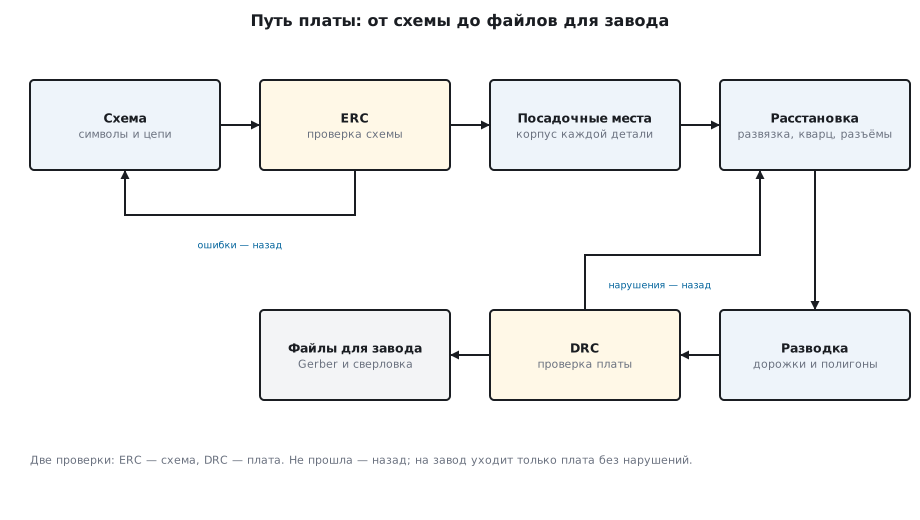
Seven steps, and two of them are checks. The schematic check (ERC) catches unconnected pins and two outputs on one net; the layout check (DRC) catches clearances, shorts, parts overlapping each other and unrouted connections. A board that has not passed DRC does not go to the factory — keep this rule as strictly as "firmware with no compiler warnings" (section 110).
130.2 Layers: two sides and a solid ground
For a board with a microcontroller running at tens of megahertz, two copper layers are usually enough: parts and signals on top, a solid ground on the bottom. A new board in KiCad is created exactly like that — two layers, 1.6 mm thick.
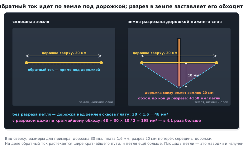
A solid ground is the main thing that makes a board quiet. A signal current returns to its source through the ground directly under its track; if the ground is cut, the return current goes around the cut, the loop grows — and pickup and emission grow with it. That is why the bottom layer is no place for tracks: one long track across the bottom layer cuts the ground in two. Four layers (signal, ground, power, signal) are needed when the board has high-speed USB, Ethernet, external memory or simply too little room.
130.3 Decoupling at every supply pin
The STM32F103 in the LQFP-48 package has four supply pins for the core and peripherals: VDD
on 24, 36 and 48 and VDDA on 9. Each one gets its own 100 nF capacitor right next to it,
and VDDA also gets 1 µF, preferably through a ferrite bead
(section 61.1). With small capacitors the point is not the capacitance but the
inductance of the path: a capacitor helps only when
the "pin — capacitor — ground" loop is short.
Three rules make sure of this:
- the capacitor sits right next to its pin, the track is straight and short; on the board from section 131 it is 2.025 mm for all four;
- the ground pin of the capacitor goes straight through a via into the solid ground;
- next to a row of pins the capacitor is placed along the normal, pointing outward: then the track does not run diagonally across neighbouring pins.
The last one is not theory. The first, naive placement on the same board gave
three shorts at the check: the supply tracks touched neighbouring GND pins
and an unused package pin (section 131.5).
Besides the decoupling at the pins there is one shared 4.7 µF capacitor on VDD; usually
it is also the bulk capacitor at the regulator output: it supplies current during load
steps until the regulator has time to respond.
Pin 1 is VBAT. If there is no battery, it is not left floating: tie it
to VDD and give it a 100 nF capacitor too.
130.4 Crystal
The crystal oscillator is the most sensitive block on the board: weak, high-impedance signals live there. The rules:
- the crystal sits close to the
OSC_IN/OSC_OUTpins, the tracks are short and equal; - under the crystal and its capacitors there is solid ground, no foreign tracks;
- the capacitors go to ground, close to the crystal.
The capacitor values are computed from the crystal's load capacitance CL given in its datasheet.
The two crystal capacitors are in series, and the stray capacitance
of the assembly and the inputs adds to them — usually 3–5 pF:
CL = C1 × C2 / (C1 + C2) + Cпар → C1 = C2 = 2 × (CL − Cпар)
Crystal CL |
Cpar 3 pF |
Cpar 5 pF |
|---|---|---|
| 12 pF | 18 pF | 14 pF |
| 18 pF | 30 pF | 26 pF |
| 20 pF | 34 pF | 30 pF |
Hence a common mistake: fitting 22 pF to a crystal with CL = 12 pF "as on every
schematic" — the oscillator drifts off frequency or does not start at all when cold.
The "Crystal" tab in the app's calculators computes the capacitors for the datasheet
CL and, the other way round, which CL the crystal sees with the capacitors already fitted.
Reset, BOOT0 and the debug connector are three blocks that on a first board are most
often done "somehow". On the F103 in LQFP-48:
BOOT0(pin 44) — a 10 kΩ resistor to ground, otherwise the chip "every other time" starts from the factory bootloader;NRST(pin 7) — a 100 nF capacitor to ground right at the pin;- the SWD connector — 3.3 V supply,
SWDIO(PA13, pin 34),SWCLK(PA14, pin 37), ground andNRST— at the board edge, with short tracks, and PA13 and PA14 are not used for anything else.
Why exactly this way — sections 61.4, 61.5 and 61.7. The training board of section 131
does without the resistor on BOOT0 and the capacitor on NRST; on your own board
you fit them.
130.5 Track width for current
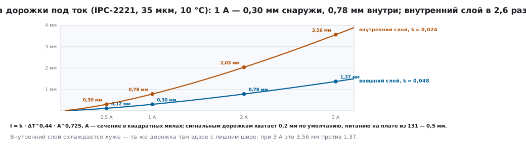
Track width is chosen by the allowed heating. The IPC-2221 standard gives
current as a function of the track cross-section A (in square mils) and the temperature rise ΔT:
I = k × ΔT^0,44 × A^0,725, k = 0,048 для внешнего слоя, 0,024 для внутреннего
For 35 µm copper and a 10 °C rise:
| Current | External layer | Internal layer |
|---|---|---|
| 0.5 A | 0.12 mm | 0.30 mm |
| 1 A | 0.30 mm | 0.78 mm |
| 2 A | 0.78 mm | 2.03 mm |
| 3 A | 1.37 mm | 3.56 mm |
For an internal layer the table asks for the same track 2.6 times wider. This is a cautious estimate with margin: later measurements showed that an internal track heats no more than an external one — the heat leaves through the dielectric into the neighbouring layers. The table gives a safe upper bound; if the internal layer is crowded, the width is recalculated using the newer charts. Signal tracks are fine with the default rules — in KiCad that is 0.2 mm width and 0.2 mm clearance; power on the board from section 131 is 0.5 mm.
130.6 Design rules and DRC
Rules are numbers that the check compares across the whole board. For a new KiCad board:
| Rule | Value |
|---|---|
| clearance between nets | 0.2 mm |
| track width | 0.2 mm |
| via | 0.6 mm, hole 0.3 mm |
| copper to board edge | 0.5 mm |
| hole to hole | 0.25 mm |
Before ordering, compare the rules with what the chosen factory can do: in cheap service tiers the minimum clearances and holes are often larger than what the program can draw.
What DRC finds can be seen from the naive placement in section 131: 20 violations of seven types — shorts by a track through foreign pins, solder mask bridges, parts on top of each other, copper at the very edge, silkscreen text on pads. After the placement was fixed — not a single one; only unrouted connections remain, and that is a separate to-do list, not a list of errors.
130.7 What goes to the factory
| File | What is in it |
|---|---|
Gerber copper F.Cu, B.Cu |
the conductor pattern |
Gerber mask F.Mask, B.Mask |
where there is no mask — the pads |
| Gerber silkscreen | the text and markings |
Gerber paste F.Paste |
the stencil for soldering |
Gerber outline Edge.Cuts |
the board shape |
| drill (Excellon) | the holes and their diameters |
job description .gbrjob |
the set and order of layers |
For the board from section 131 that is 10 files. Exporting "all layers" gives 25 files — 24 layers together with auxiliary ones that the factory does not need and that only confuse it. For assembly at the factory a bill of materials (BOM) and a placement coordinate file for the pick-and-place machine are added.
130.8 Pitfalls
| Symptom | Cause |
|---|---|
| glitches and noise "out of nowhere" | the ground is cut by bottom-layer tracks |
| reset when a load switches on | decoupling far from the pin, or the capacitor's ground through a long track |
| DRC: short at the package | a track from a decoupling capacitor runs diagonally across neighbouring pins |
| the crystal does not start when cold | the capacitors do not match the CL of that crystal |
| the chip "every other time" starts in the bootloader | BOOT0 is floating: no 10 kΩ resistor to ground |
| a power track gets hot | width not chosen for the current, especially on an internal layer |
| the factory rejects the order | the board rules are finer than the factory can make |
| "extra layers" at the factory | all layers exported instead of the needed ones |
130.9 Summary
- Two sides: parts and signals on top, solid ground on the bottom — do not cut it.
- 100 nF decoupling at every supply pin: on the LQFP-48 F103 that is 24, 36, 48 and
VDDA9; along the normal, short, ground straight into a via. - Crystal capacitors:
C1 = C2 = 2 × (CL − Cpar); 18 pF → 26–30 pF. BOOT0— 10 kΩ to ground,NRST— 100 nF at the pin, the SWD connector at the board edge, PA13 and PA14 left free.- Width for current per IPC-2221: 1 A at 10 °C — 0.30 mm outside, 0.78 mm inside.
- KiCad default rules are 0.2 mm; check them against the factory before ordering.
- To the factory — 10 files: eight layers, the job file and the drill file.
Next: section 130а "How to read a schematic: symbols, nets, sheets" — symbols, letters, nets and sheets: how to find on someone else's schematic where a pin goes.