 Embedded HandbookApps
1. The microcontroller as such
Before blinking an LED, it helps to understand what exactly you are controlling. This section is about what lies beneath all the others: the core, the memory, the instruction set. Without it the later sections would have to be taken on faith.
Terms used in the documentation
Term Meaning MCU (microcontroller unit) a microcontroller: core, memory and peripherals on one die core, processor the core, the processing part peripheral a peripheral block: a timer, an ADC, a UART RISC (reduced instruction set computer) a set of simple instructions of equal length architecture (ARMv7-M) the architecture: a specification of instructions and the execution model licensee a manufacturer that has bought a licence for the core core registers (R0–R12, SP, LR, PC, xPSR) the registers of the core memory map which addresses belong to what memory management unit (MMU) translates virtual addresses into physical ones; Cortex-M has none bit-band region, alias region the bit-banding region and its bit-by-bit mirror Thumb-2 instruction set the Thumb-2 instruction set: 16- and 32-bit instructions mixed together pipeline: fetch, decode, execute the stages of the instruction pipeline
1.1 What it is in the first place
A microcontroller (MCU, Micro Controller Unit) is a digital chip that gathers on one die everything needed to work on its own:
- the core — the arithmetic logic unit and control;
- RAM — working memory for data;
- ROM (Flash) — non-volatile memory for the program;
- peripherals — ADC, DAC, UART, SPI, I²C, timers and so on.
The key difference from a processor: a processor usually has no Flash and RAM on the die — they are placed outside to make manufacturing cheaper and simpler. A microcontroller is self-sufficient: apply power and it runs.
The second difference matters more to a programmer than the first — the memory management unit (MMU). A processor running Linux or Windows translates addresses: each program has its own virtual address space, the MMU maps it on the fly onto physical memory and keeps the program out of other programs' pages. Processes, memory protection and swapping rest on this. A microcontroller has no MMU: an address in the program is the physical address, and the program sees all the memory at once. Some Cortex-M have an MPU — it forbids access to regions but does not translate addresses (section 11а). That is why ordinary Linux does not run on a Cortex-M (section 191.1); what runs on it is "bare-metal" firmware or an RTOS.
The first single-chip microcontrollers appeared in the 1970s: the TMS1000 from Texas Instruments and the 8048 from Intel.
Two popular core architectures
| ARM | RISC-V | |
|---|---|---|
| expansion | Advanced RISC Machine | reduced instruction set computer |
| licence | proprietary, royalties to ARM Holdings | open and free |
| niche | from MCUs to servers and the Apple M1 | low-cost MCUs, custom cores |
Both are RISC: the instructions are encoded so that they decode simply and execute quickly.
1.2 ARM, Cortex and who does what
It is easy to get confused here, so let us lay it out in layers.
The ARM architecture (ARMv6-M, ARMv7-M, ARMv8-M…) is a specification: the instruction set, the execution model, the memory organisation, the cost of instructions in cycles. Not hardware, but a document. A compiler that can generate code for an architecture can do so for all processors that implement it.
A Cortex-M core is a concrete implementation of the architecture, a ready-made block to be embedded in a die. The Cortex-M3, for example, is designed to ARMv7-M, and the Cortex-M4 to ARMv7E-M: the same architecture plus an extension with DSP instructions. People often simply write "the M4 is ARMv7-M", but the letter E in the name stands precisely for the added digital signal processing instructions.
A microcontroller is the core plus what the silicon vendor has added around it: Flash, RAM, peripherals, buses. This is the work of ST, NXP, TI, Mikron, Milandr and dozens of others. ARM Holdings itself manufactures nothing — it licenses the architecture and the cores.
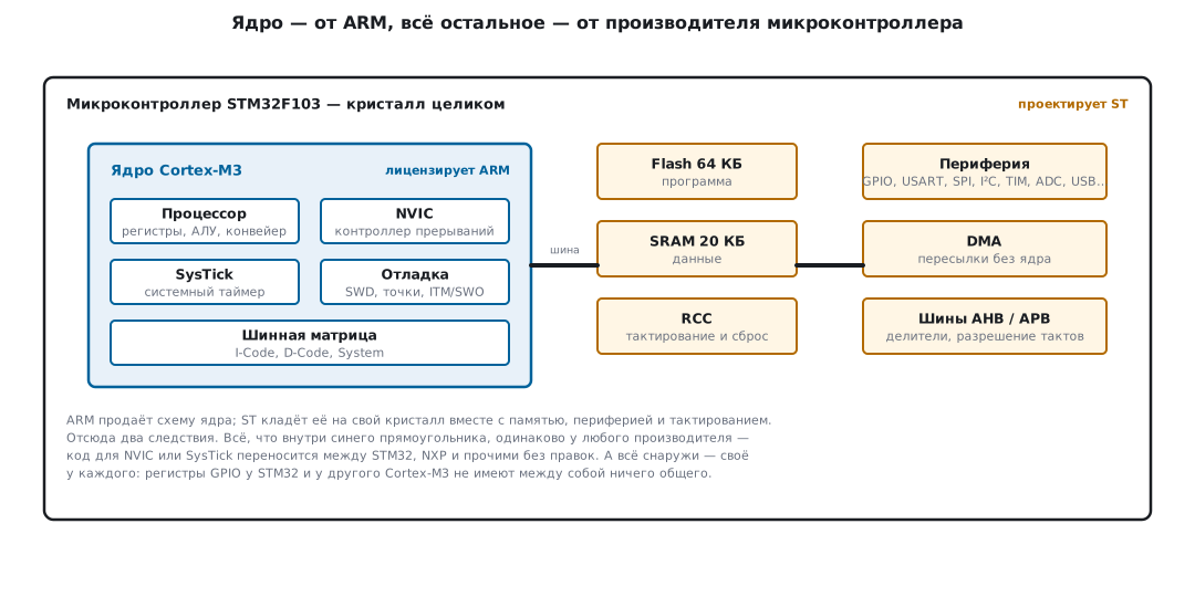 A Cortex-M3 core inside a microcontroller built on it
An important consequence: having the core does not guarantee having the feature. The Cortex-M3 is designed with bit-banding support, but implementing it is the vendor's decision. The STM32F1 implements it, while the Cortex-M7 has none at all. Always check the reference manual of the specific MCU, not the description of the core.,
Three Cortex families
| Family | Letter | What for |
|---|---|---|
| Cortex-A | Application | heavy computing, operating systems (Linux, Android): phones, tablets, single-board computers |
| Cortex-M | eMbedded | embedded tasks: IoT, motor control, meters, household appliances, medical equipment |
| Cortex-R | Real-time | systems where fault tolerance and a guaranteed response time matter |
We are interested in Cortex-M.
Cortex-M3 versus Cortex-M4: what moving to F4 really gives you
The two reference platforms of this handbook are the STM32F103 (Cortex-M3) and the STM32F407/F401 (Cortex-M4). The difference between them is not cosmetic.
| Cortex-M3 (F1) | Cortex-M4 (F4) | |
|---|---|---|
| architecture | ARMv7-M | ARMv7E-M |
| clock frequency | up to 72 MHz | up to 180 MHz (F427/F429/F446/F469), 168 MHz (F405/F407), 84–100 MHz (F401/F410/F411) |
| FPU | no | present on all STM32F4, single precision |
| DSP instructions | no | yes: single-cycle MAC, saturating arithmetic, SIMD |
| pipeline | 3 stages | 3 stages |
| bit-banding | yes | yes |
| Flash accelerator | prefetch buffer | ART Accelerator — an instruction cache, zero wait states |
| GPIO port bus | APB2 | AHB1 |
| DMA | 7+5 channels, no FIFO | 2 controllers × 8 streams, FIFO, burst |
What this means in practice.
Floating point. On the M3 every float multiplication is a call to a library function
taking dozens of cycles. On the M4 with an FPU it is one instruction. For controllers, filters
and sensor reading conversion the difference is an order of magnitude. But the FPU has to be enabled —
it is off after reset — and the compiler has to be told -mfpu=fpv4-sp-d16
-mfloat-abi=hard, otherwise you get an M4 that computes like an M3.
DSP instructions. Single-cycle multiply-accumulate, saturating arithmetic (the result does not overflow but stops at the limit) — the things the CMSIS-DSP library is built on: FFT, FIR and IIR filters, matrices. The M3 can compute the same, but several times slower.
ART Accelerator. At 168–180 MHz the Flash physically cannot deliver instructions fast enough — wait states are needed. ART caches instructions and branches so that during linear execution there are practically no waits. That is why the F407 at 168 MHz gives about 210 DMIPS — the same 1.25 DMIPS per megahertz as the F103 at 72 MHz (90 DMIPS): performance grows with frequency even though the Flash needs five wait states. Without ART, at the same 168 MHz the core would spend most of its time waiting for Flash.
⚠️ The main trap of moving F1 → F4 lies not in the core but in the peripherals: different clock buses (
AHB1ENRinstead ofAPB2ENR), different base addresses, a different GPIO register model, a different DMA. Code that works with the core — NVIC, SysTick, bit-banding — moves over without changes. Code that works with the peripherals is rewritten almost entirely. The details for each peripheral are in the corresponding sections.
1.3 Core registers
Cortex-M is a load/store machine: arithmetic is performed only on registers, and memory is accessed by separate load and store instructions.
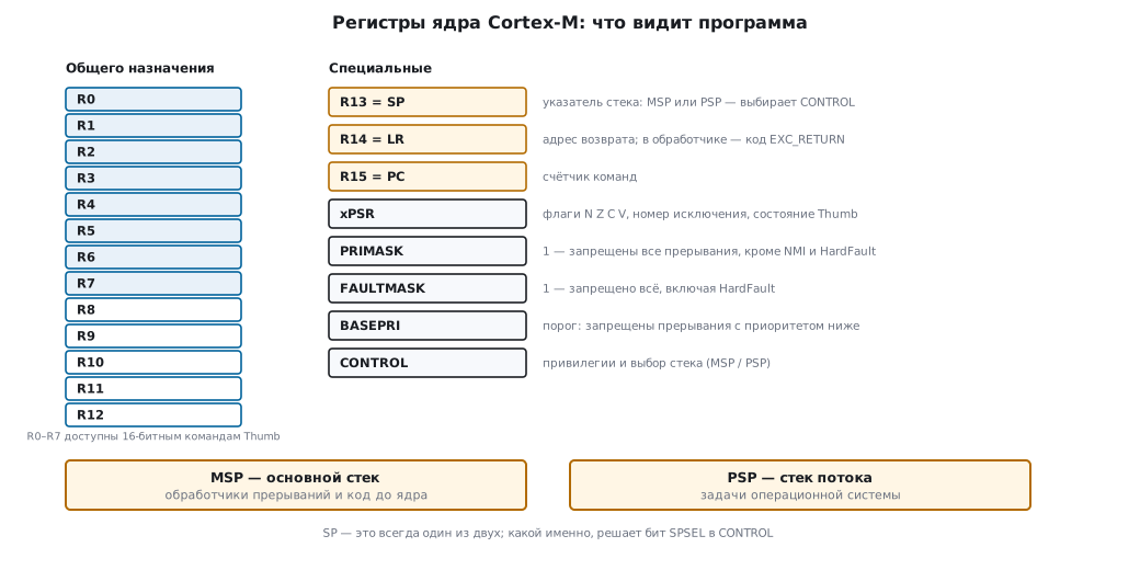 Cortex-M core registers
| Register | Purpose |
|---|---|
R0–R12 |
general purpose; the compiler uses some of them for its own needs |
R13 (SP) |
the stack pointer, banked — changes when the CPU mode changes |
R14 (LR) |
the return address from a subroutine |
R15 (PC) |
the program counter |
xPSR |
the program status flags |
A "banked" SP means that there are physically two stack pointers — MSP and PSP.
Exception handlers always run on MSP, while the main code runs on MSP after
reset or on PSP if the SPSEL bit is set in the CONTROL register. Privilege
is set by a separate bit of the same register (nPRIV), and the choice of stack does not depend on it.
Task switching in an RTOS is built on the two stacks: each task has its own PSP,
while interrupts run on the shared MSP. More in section 26.
What it looks like in real life. Simple C code:
uint8_t a, b, c;
a = 3;
b = 2;
c = a * b;
compiles into roughly this (Thumb, no optimisation, for Cortex-M4):
movs   r3, #3         ; занести 3 в r3
strb   r3, [r7, #7]   ; сохранить r3 в переменную a
movs   r3, #2         ; занести 2 в r3
strb   r3, [r7, #6]   ; сохранить r3 в переменную b
ldrb   r2, [r7, #7]   ; загрузить a в r2
ldrb   r3, [r7, #6]   ; загрузить b в r3
smulbb r3, r2, r3     ; умножить, результат в r3
strb   r3, [r7, #5]   ; сохранить результат в c
smulbb multiplies the lower 16-bit halves; it is one of the Cortex-M4 DSP instructions.
The Cortex-M3 (F103) has no such instruction; in its place there will be mul r3, r2, r3.
Not a single operation is performed "in memory" — everything goes through the registers. Hence a practical conclusion: the fewer unnecessary memory accesses in a hot loop, the faster the code.
1.4 The memory map
A Cortex-M address is 32 bits wide, so there are exactly 2³² = 4 294 967 296 addresses — that is
4 GB: the last byte has the number 0xFFFF FFFF, nothing more fits in 32 bits.
ARM divides this space into regions the same way on all Cortex-M from any
vendor: code at the bottom, SRAM from 0x2000 0000, peripherals from 0x4000 0000, core
registers at the top. Only core code is portable because of this — more on it right below the table.
The peripherals inside their region differ for each vendor and even for each STM32
family: a port, a timer or a UART does not move from F1 to F4 without changes (section 1.10).
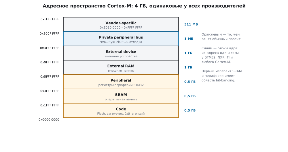 The fixed map of the Cortex-M address space
| Range | Size | What is there |
|---|---|---|
0x0000 0000 … |
512 MB | code: the vector table, the initial stack pointer, the program |
0x2000 0000 … |
512 MB | internal SRAM |
0x4000 0000 … |
512 MB | peripherals |
0x6000 0000 … |
2 GB | external memory through FSMC/EMI |
0xE000 0000 … |
512 MB | registers of the Cortex core itself (NVIC, SysTick, debug) |
The core registers sit at fixed addresses on all Cortex-M — which is why code that works with the NVIC or SysTick moves over without changes.
The code region on STM32
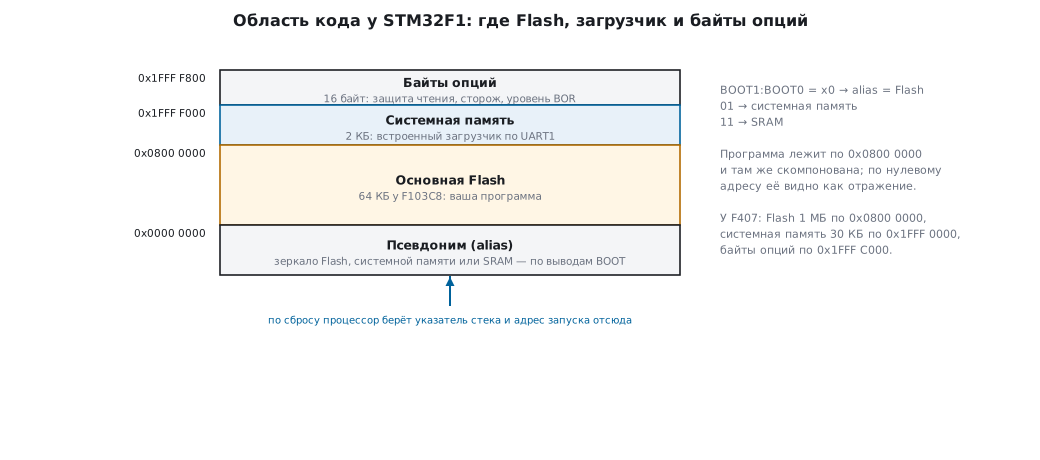 Layout of the code region on STM32
Internal Flash on all STM32 lives from address 0x0800 0000. At the same time it is
duplicated ("aliased") from address 0x0000 0000 — depending on the boot
setting. One and the same function is accessible both as 0x0800 16DC and as 0x0000 16DC.
Then come two service regions:
- System memory — ROM with the factory bootloader: the board is flashed without a programmer.
The bootloader interfaces depend on the family: on the F103C8 (BluePill) only
USART1onPA9/PA10, on the F105/F107 and F405/F407 USB DFU and CAN are added, on the F401 — USB DFU, I²C and SPI. Details in sections 4.9 and 11. - Option bytes — MCU configuration flags: Flash read protection, the hardware watchdog, the boot mode.
How much SRAM there really is
The SRAM region begins at 0x2000 0000, but the real end depends on the amount of memory
in your chip. For an STM32F103RB with 20 KB:
20 КБ = 20 × 1024 = 0x5000 байт
последний адрес = 0x2000 0000 + 0x4FFF = 0x2000 4FFF
An access beyond this boundary raises a Bus Fault exception.
1.5 Bit-banding
The problem
Changing a single bit of a variable is something you do all the time:
uint8_t temp = 0;
temp |= 0x4;     // установить бит 2
temp &= ~0x4;    // сбросить бит 2
Each such line turns into three instructions — load, modify, store:
ldrb   r3, [r7, #7]
orr.w  r3, r3, #4
strb   r3, [r7, #7]
Hence two troubles. The first is wasted cycles. The second is more serious: between the read and the write an interrupt or a task switch may squeeze in and change the same word — and your write will overwrite the other change. A classic race.
The solution
Bit-banding maps each bit of a special memory region onto a whole word in another, "mirror" region. Write the word — exactly one bit changes, in one operation, without races.
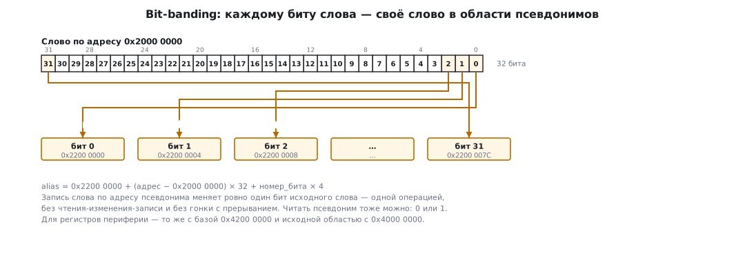 Mapping the bits of address
0x2000 0000 into the bit-band region
The conversion formula:
alias_адрес = база_alias + (смещение_в_области × 32) + (номер_бита × 4)
The two regions on Cortex-M3/M4:
| What | bit-band region | alias region |
|---|---|---|
| SRAM | 0x2000 0000–0x200F FFFF (1 MB) |
0x2200 0000–0x23FF FFFF (32 MB) |
| peripherals | 0x4000 0000–0x400F FFFF (1 MB) |
0x4200 0000–0x43FF FFFF (32 MB) |
The 1 MB ↔ 32 MB ratio is easy to explain: each bit of the source region corresponds to a whole 32-bit word in the alias.
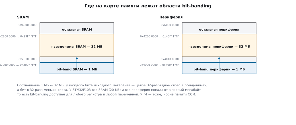 The bit-banding regions on the overall memory map
Macros
#define BITBAND_SRAM_BASE   0x20000000u
#define ALIAS_SRAM_BASE     0x22000000u
#define BITBAND_SRAM(a, b)  ((ALIAS_SRAM_BASE + (((uint32_t)&(a)) - BITBAND_SRAM_BASE) * 32u + ((b) * 4u)))

#define BITBAND_PERI_BASE   0x40000000u
#define ALIAS_PERI_BASE     0x42000000u
#define BITBAND_PERI(a, b)  ((ALIAS_PERI_BASE + (((uint32_t)(a)) - BITBAND_PERI_BASE) * 32u + ((b) * 4u)))
Blinking the LED on PC13 (STM32F103) without a read-modify-write operation:
volatile uint32_t *pc13 = (uint32_t *)BITBAND_PERI(&GPIOC->ODR, 13);
*pc13 = 1;      /* одна запись — один бит */
Let us check by hand: the GPIOC base on F1 is 0x4001 1000, the ODR offset is 0x0C.
смещение   = 0x4001100C − 0x40000000 = 0x1100C
alias      = 0x42000000 + 0x1100C × 32 + 13 × 4 = 0x4222 01B4
⚠️ Addresses from other people's examples do not carry over. Guides often show the calculation for
GPIOA->ODRat address0x4002 0014— that is the STM32F4. On the STM32F1 the port bases are different (GPIOA=0x4001 0800), and theODRoffset is0x0C, not0x14. Copy such an address to F1 and you will miss the register. Always compute the address from&GPIOx->ODR, not from a constant.⚠️ The bit number depends on which address you substituted. For a byte address the bit numbers run 0…7, for a word address 0…31. Both give the same alias address (4 bytes × 32 = 32 bits × 4), but mixing up the ranges is easy: byte
0x400F FFFFwith "bit 31" runs past the end of the alias region.⚠️ Bit-banding does not do away with the read. The bus itself performs a write to the alias as a read-modify-write of the whole register. This protects against interrupts, but not against the peripheral itself. In a register of flags that are cleared by writing a one (
EXTI->PR), writing a one to a single bit reads all the pending flags and writes them back as ones — all waiting lines get cleared, the same mistake as withEXTI->PR |=(section 7.9). In a register where a flag is cleared by writing a zero (TIMx->SR), a flag that the hardware raises between the read and the write gets erased. Such flags are cleared by writing the mask directly:EXTI->PR = EXTI_PR_PR3,TIM2->SR = ~TIM_SR_UIF.⚠️ Bit-banding is not everywhere. It is absent on the Cortex-M0/M0+, absent on the Cortex-M7 (F7, H7) and on ARMv8-M cores — the Cortex-M33 and newer (L5, U5, H5, WBA). Code with bit-banding will not port to these families; there a bit can be changed atomically through
BSRRfor pins,LDREX/STREX(except M0/M0+) or a critical section.
1.6 Thumb-2 and alignment
Why Thumb was needed
ARM historically has 32-bit instructions: a rich set and good performance, but every instruction takes 4 bytes of Flash. Flash is die area, which means price and power consumption.
Thumb is a 16-bit set, a subset of the most frequently used instructions. They are transparently expanded into 32-bit ones at execution, with no loss of speed. Thumb code takes about 65 % of the size of ARM code. The price is reduced capabilities: only branches can be conditional, and many instructions see only half of the registers.
Thumb-2 mixes 16- and 32-bit instructions in one mode: code density like Thumb, completeness of the set almost like ARM. The Cortex-M3/M4/M7 support it in full, and the M4/M7 add instructions for floating-point numbers.
Alignment
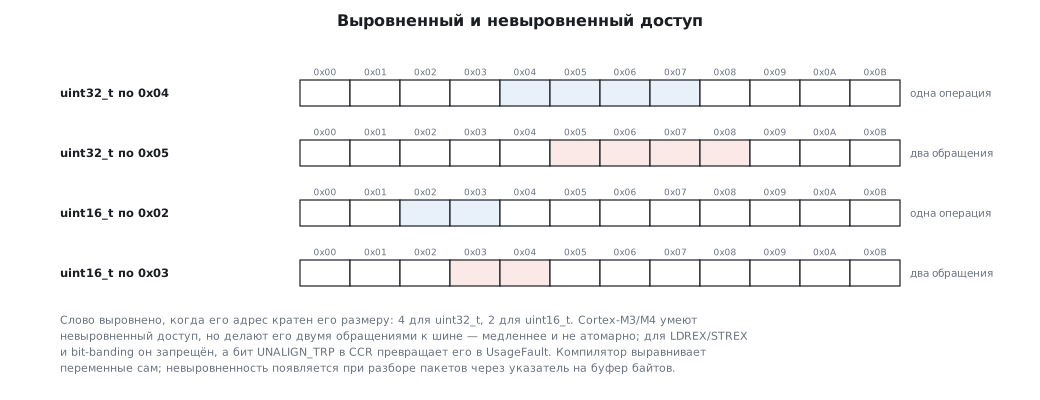 Aligned and unaligned access
Aligned access means that a 32-bit variable sits at an address that is a multiple
of 4 (0x2000 0000, 0x2000 0004…), a 16-bit one at a multiple of 2. Early ARMs could not do otherwise,
and this fragmented memory: unused bytes were left between variables.
The Cortex-M3/M4/M7 support unaligned access: the LDR/STR instructions and their
halfword variants also work with an address that is not a multiple of the size. The compiler
still aligns variables and structure fields. Data is packed tightly only
in a packed structure (__attribute__((packed))), for example when parsing a packet.
An unaligned access costs more — the bus makes two accesses — and is not atomic.
The Cortex-M0/M0+ have no such access at all, there you get a HardFault; on the M3/M4 it can be
turned into a fault with the UNALIGN_TRP bit in SCB->CCR.
⚠️ Unaligned access is allowed not for all instructions — only
LDR,LDRT,LDRH,LDRHT,LDRSH,LDRSHT,STR,STRT,STRH,STRHT. The others give a UsageFault exception on an unaligned address. Remember separately: peripheral registers almost always require whole-word access. For the STM32F1 GPIO, halfword or byte access is forbidden explicitly in the documentation.
1.7 The pipeline
Executing an instruction is not one step: first it has to be fetched from memory (fetch), then decoded (decode), and only then executed (execute). If this is done sequentially, the processor sits idle most of the time.
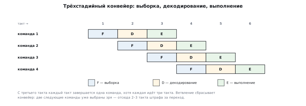 A three-stage instruction pipeline
The pipeline executes the stages of different instructions in parallel: while one is being executed, the next is being decoded, and a third is being fetched.
| Core | Stages |
|---|---|
| Cortex-M0+ | 2 (fewer stages mean less energy, which matters for low-power MCUs) |
| Cortex-M0/M3/M4 | 3 |
| Cortex-M7 | 6 |
The price of the pipeline is branches. When the program takes a conditional branch, the instructions already loaded into the pipeline turn out to be unneeded and are discarded (the "branch shadow"). Hence a practical conclusion for hot loops: fewer unpredictable branches mean denser pipeline work.
1.8 What it is written in
The C language, created by Dennis Ritchie in the 1970s, remains the main tool: more than 80 % of microcontroller system code is written in it.,
Why exactly C:
- Compiled and efficient — machine code, high performance, compact programs. In embedded systems, where resources are tightly limited, this is decisive.
- Low-level — it lets you work at the register level and optimise for specific hardware.
- Portable — code moves between platforms.
A study by the universities of Minho, Nova de Lisboa and Coimbra covering 27 languages showed that C is the most energy-efficient and the fastest in execution time.
C++ is used where graphics and a complex interface are needed — ST's TouchGFX library for high-resolution displays is built on it.
1.9 The same Cortex-M3, but domestic: 1986VE9x
A useful exercise for understanding where the core ends and the vendor begins: the Russian microcontroller 1986VE9x (Milandr) is built on the same ARM Cortex-M3 core as the STM32F1.
| 1986VE9x | STM32F103C8 | |
|---|---|---|
| core | Cortex-M3 | Cortex-M3 |
| clock frequency | up to 80 MHz | up to 72 MHz |
| Flash | 128 KB | 64/128 KB |
| RAM | 32 KB | 20 KB |
| ADC | 2 × 12 bit, up to 0.5 Msps, 16 channels | 2 × 12 bit, 1 Msps |
| DAC | 2 × 12 bit | not on the C8 |
| oscillators | HSI 8 MHz, LSI 40 kHz, HSE 2…16 MHz, LSE 32 kHz | HSI 8 MHz, LSI 40 kHz, HSE 4…16 MHz, LSE 32.768 kHz |
| supply | 2.2–3.6 V, built-in 1.8 V regulator | 2.0–3.6 V |
| backup domain | yes, with RTC | yes, with RTC |
Almost everything matches except the names of the peripheral registers: on the Milandr part pin configuration
is set by separate registers OE, FUNC, ANALOG, PULL, PWR, not by the
MODE/CNF pair as on the STM32F1.
What follows from this. Everything that belongs to the core — registers R0–R15, the memory
map, NVIC, SysTick, Thumb-2, the pipeline — carries over one to one. Everything that
belongs to the peripherals does not carry over at all. The boundary between "knowledge about ARM"
and "knowledge about STM32" runs exactly here.
1.10 Pitfalls
Code from F1 "almost" ports to F4, but the peripherals stay silent. The core is the same, but the clock buses, base addresses, GPIO and DMA differ: core code (NVIC, SysTick) carries over, peripheral code is rewritten (1.2).
A write to an address from someone else's example does nothing. Address 0x4002 0014 is GPIOA->ODR on F4; on F1 the port base
and offset are different. The address is taken as the expression &GPIOx->ODR, not as a number (1.5).
Bit-banding goes beyond the region. The bit number for a byte address is 0…7, for a word 0…31; mix them up and you miss the alias region (1.5).
Code with bit-banding builds on F7/H7 but does not work. To the compiler the alias address is an ordinary number, but the Cortex-M0/M0+, M7 and M33 have no such region: the write goes nowhere or ends in a bus fault (1.5).
A UsageFault out of nowhere. Unaligned access is allowed only for LDR/STR and their variants; peripheral
registers only as whole words, on F1 GPIO halfword and byte access is forbidden (1.6).
1.11 Summary
- Microcontroller = core + Flash + RAM + peripherals on one die; a processor places memory outside.
- ARM sells the architecture and cores; the silicon is made by ST, Milandr and others. The core defines the instruction set and the memory map, the vendor defines the peripherals.
- A feature in the core description does not mean the feature is in your MCU: bit-banding exists on the M3/M4, not on the M0/M0+, M7 and M33.
- The 4 GB address space is the same on all Cortex-M; the core registers are always at the same addresses — hence the portability of system code.
- Flash on STM32 begins at
0x0800 0000and is duplicated from0x0000 0000. - Bit-banding replaces "read-modify-write" with one atomic write, but addresses
must be computed from the real
&GPIOx->ODR, not from a ready-made constant. - Cortex-M runs in Thumb-2; unaligned access is allowed, but not for all instructions and almost never for peripheral registers.
Next: section 2 "The STM32 portfolio and choosing a chip" — how to choose the right one from over two thousand microcontrollers and what the letters in the part number mean.