 Embedded HandbookApps
17. The I²C bus
Two wires, up to a hundred devices, any distance within a board — and a well-earned reputation as the most capricious peripheral. This is where you find most of the cases where everything was done "by the documentation" and the bus is dead stuck.
Terms used in the documentation
Term Meaning master / slave the device that drives the clock / the device that answers start / repeated start condition the start condition / a start without a preceding stop acknowledge ( ACK) / not acknowledge (NACK)the receiver confirms / refuses a byte clock stretching the slave holding the clock low arbitration lost another master won the bus bus busy the bus is taken open-drain an output that can only pull the line low rise time ( TRISE)the rise time of an edge address matched ( ADDR)the address was recognised EEPROM electrically erasable non-volatile memory page write writing a whole page in one transfer write cycle time ( tWR)the duration of the internal write cycle acknowledge polling polling for readiness by the acknowledge SMBus, packet error checking (PEC) the system management bus, the checksum of a transfer
17.1 How it is built
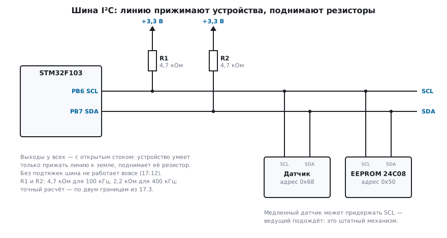
Two wires: SCL — the clock, SDA — the data. Both outputs of all devices are open-drain: a device can only pull the line to ground, and an external resistor pulls it up.
Three consequences follow at once that determine everything else:
Pull-up resistors are mandatory. Without them the lines will never rise to one, and the bus simply will not work. The typical value is 4.7 kΩ for 100 kHz, 2.2 kΩ for 400 kHz. Ready-made sensor modules usually already have them, but if there are several modules on the bus, their resistors end up in parallel — the total resistance drops, and the line becomes hard to pull down.
Any device can "hold" the clock. A slow sensor holds SCL low and makes the master wait. This is a standard mechanism, not a failure.
One stuck device blocks everyone. If a slave is reset in the middle of a transfer and is left holding SDA, the bus is dead for all participants. The cure is the technique from 17.6.
17.2 Addressing and a transaction
The address is seven bits — that is, up to 128 addresses, some of which are reserved. It is put into the register shifted left by one bit, and the lowest bit indicates the direction:
| Action | Byte on the line |
|---|---|
write to device 0x68 |
0xD0 |
read from device 0x68 |
0xD1 |
⚠️ Half of the "sensor does not answer" problems are confusion between the seven-bit address and the already shifted eight-bit one. Sensor documentation uses both variants, and
0x68and0xD0describe the same device.
The "I²C address" tab in the app's calculators converts an address into line bytes in both directions and splits a ten-bit address into two bytes.
The ten-bit address. Seven bits are not enough for everyone, and the standard has a second
kind of address — ten-bit, that is 1024 addresses. There is no separate line for it:
the address is split over two bytes, and the marker is the reserved combination
of upper bits 11110.
| Step | Byte on the line | What is in it |
|---|---|---|
| start | 0xF2 |
11110 + the two upper address bits (01) + the write bit |
| second byte | 0xA5 |
the eight lower address bits |
| repeated start | 0xF3 |
the same upper bits, but the read bit |
In the example the address is 0x1A5. There is no direct "read at a ten-bit address":
the device must first hear both bytes in write mode and remember that it is
being addressed, and only then a repeated start with the same header
turns the transfer around. That is why a read costs 18 bit clocks more
than a seven-bit one — at 400 kHz that is an extra 45 µs per transfer.
Four seven-bit addresses 0x78…0x7B went to the header — no device on the same bus
may use them as ordinary addresses.
In the peripheral this is one bit. In the old-style I²C (F1, F4) the ADDMODE bit in I2C_OAR1
makes the slave's own address ten-bit. The master sends a ten-bit
address in software: the header into DR, the ADD10 flag in SR1, then the second byte
and the ADDR flag. In the new-style
block (F0, G0 and later) the master has two bits in CR2: ADD10 — the address
is ten-bit, and HEAD10R — send only the header before a read, without
the second byte, if the device has already been selected by the previous transfer.
⚠️ Ten-bit sensors hardly exist: the mass-market small parts live in seven bits. If you see
0xF2on the analyzer screen, do not look for a device with address0x79— it is a header, and the real address is in the next byte.
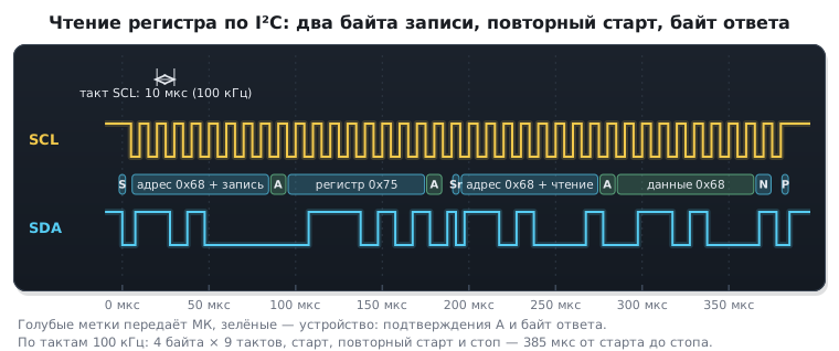
A typical sensor register read consists of two transactions in a row:
- start → address with the write bit → register number;
- repeated start → address with the read bit → receive data → stop.
A repeated start instead of "stop plus start" matters: it does not release the bus, and another master cannot squeeze in between the request and the answer.
This is what reading register 0x75 of device 0x68 looks like on the analyzer screen; the labels above SDA
show who transmits each byte:
17.3 Configuration
void i2c1_init(void)
{
    RCC->APB2ENR |= RCC_APB2ENR_IOPBEN | RCC_APB2ENR_AFIOEN;
    RCC->APB1ENR |= RCC_APB1ENR_I2C1EN;

    /* PB6 (SCL) и PB7 (SDA): альтернативная функция, ОТКРЫТЫЙ СТОК. */
    GPIOB->CRL &= ~(GPIO_CRL_MODE6 | GPIO_CRL_CNF6 |
                    GPIO_CRL_MODE7 | GPIO_CRL_CNF7);
    GPIOB->CRL |= GPIO_CRL_MODE6 | GPIO_CRL_CNF6;    /* 11 -> AF open-drain */
    GPIOB->CRL |= GPIO_CRL_MODE7 | GPIO_CRL_CNF7;

    I2C1->CR1 &= ~I2C_CR1_PE;             /* настраивать только выключенным */

    I2C1->CR2 = APB1_MHZ;                 /* частота шины, НЕ скорость I2C */
    I2C1->CCR = APB1_HZ / (2u * 100000u); /* делитель: 180 для 100 кГц */
    I2C1->TRISE = APB1_MHZ + 1u;          /* максимальное время фронта */

    I2C1->CR1 |= I2C_CR1_PE;
}
⚠️ The output must be open-drain. Configure
push-pull— and the microcontroller will start actively driving the line high, fighting the sensor that pulls it low. Sometimes this even "works" until the first conflict, after which the output stages burn out.
Three numbers that get confused:
| Register | What it means |
|---|---|
CR2.FREQ |
the frequency of the APB1 bus in megahertz (not the I²C speed) |
CCR |
the divider that sets the bus speed |
TRISE |
the maximum allowed edge rise time in clock cycles |
The divider calculation:
стандартный режим (100 кГц):  CCR = Fpclk / (2 × Fscl)                → 180 при 36 МГц
быстрый режим (400 кГц):      CCR = I2C_CCR_FS | Fpclk / (3 × Fscl)   → 30 при 36 МГц
In fast mode the F/S bit (I2C_CCR_FS,
bit 15) must be added to the divider: with DUTY = 0 (bit 14) the low level is twice as long as the high one —
hence the three in the formula. Without F/S the same number 30 gives standard mode with
equal half-periods: 36 MHz / (2 × 30) = 600 kHz — outside any standard.
TRISE is computed from the maximum edge time: 1000 ns for standard
mode gives FREQ + 1, and 300 ns for fast mode gives about a third of that.
Too large a value makes the bus slower than stated, too
small a value leads to failures on long lines.
The pull-up: between two limits
The resistor cannot be "any": it is bounded from below by the current the output can sink, and from above by the line capacitance it must charge within the allotted edge time.
From below. While some device holds the line at zero, a current
(VDD − VOL) / Rp flows through the resistor, and it must not exceed what
the weakest output on the bus can sink. For an STM32F411 pin the datasheet gives VOL ≤ 0.4 V
at 8 mA, but a sensor on the same bus may be weaker — a margin is usually
taken. Any standard-mode and fast-mode device must sink
3 mA at 0.4 V, so Rp ≥ (VDD − 0.4 V) / 3 mA: 0.97 kΩ at 3.3 V
and 1.53 kΩ at 5 V. Hence the familiar "not below 1 kΩ" at 3.3 V (a current of 2.9 mA).
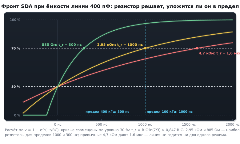
From above. The rising edge is formed only by the resistor, while the output actively discharges
the line; the rise time between the 30 and 70 % levels is t_r = Rp · Cb · ln(7/3)
≈ 0.85 · Rp · Cb. The F411 datasheet sets the limit: line capacitance up to 400 pF,
an edge no longer than 1000 ns in standard mode and 300 ns in fast mode. Hence:
| Mode | t_r limit |
Rp at 400 pF, no more than |
|---|---|---|
| 100 kHz | 1000 ns | 2.95 kΩ |
| 400 kHz | 300 ns | 885 Ω |
The usual 4.7 kΩ on a long 400 pF line gives a 1.6 µs edge — such a bus fits neither fast mode nor standard mode (limit 1000 ns), and this is not a configuration error but physics. A short bus on a board is tens of picofarads, and there 4.7 kΩ passes with a margin. The lower the resistance, the steeper the edges and the better the noise immunity, but the higher the current at zero; the smallest value that the lower limit allows is chosen.
17.4 🔧 Reading a sensor register
uint8_t i2c1_read_reg(uint8_t addr7, uint8_t reg, uint8_t *value)
{
    /* 1. Старт. */
    I2C1->CR1 |= I2C_CR1_START;
    while (!(I2C1->SR1 & I2C_SR1_SB)) { }

    /* 2. Адрес в режиме записи. */
    I2C1->DR = (uint8_t)(addr7 << 1);
    while (!(I2C1->SR1 & I2C_SR1_ADDR)) { }
    (void)I2C1->SR1;                      /* сброс ADDR: сначала SR1... */
    (void)I2C1->SR2;                      /* ...затем SR2 */

    /* 3. Номер регистра. */
    while (!(I2C1->SR1 & I2C_SR1_TXE)) { }
    I2C1->DR = reg;
    while (!(I2C1->SR1 & I2C_SR1_BTF)) { }

    /* 4. Повторный старт, адрес в режиме чтения. */
    I2C1->CR1 |= I2C_CR1_START;
    while (!(I2C1->SR1 & I2C_SR1_SB)) { }
    I2C1->DR = (uint8_t)((addr7 << 1) | 1u);
    while (!(I2C1->SR1 & I2C_SR1_ADDR)) { }

    /* Единственный байт: снять подтверждение ДО сброса ADDR. */
    I2C1->CR1 &= ~I2C_CR1_ACK;
    (void)I2C1->SR1;
    (void)I2C1->SR2;
    I2C1->CR1 |= I2C_CR1_STOP;

    while (!(I2C1->SR1 & I2C_SR1_RXNE)) { }
    *value = (uint8_t)I2C1->DR;

    I2C1->CR1 |= I2C_CR1_ACK;
    return 0u;
}
Two non-obvious things are hidden here, and each of them hangs the bus.
⚠️ The
ADDRflag is cleared by reading two registers in a row — firstSR1, thenSR2. Read only one — the flag stays, and the bus is stuck. How the documentation denotes such behaviour was covered in section 39.⚠️ When reading a single byte the acknowledge is removed in advance — before clearing
ADDR, not after reception. Otherwise the device will send a second byte you are not expecting, and the bus loses synchronisation.
Timeouts are mandatory in production code. All the while (!(flag)) loops above
are shown without them for readability, but in a product each such loop is a potential
eternal hang: it is enough for one wire to come off. In the verification file
for this section the timeouts are there, and the function returns the number of the step at which
everything stopped — this greatly speeds up troubleshooting.
17.5 ⚠️ Known bugs of the peripheral itself
A separate case where it is not your code that is to blame. For the I²C in the F1 the device errata
describes the bus busy flag getting stuck: after a glitch
on the line the BUSY flag stays set, and any attempt to start a transfer
is ignored. The errata for the F405/F407 (ES0182) has no such item — there
the I²C has its own bugs (section 39б) — but the same state can occur in any series
if a slave got stuck in the middle of a byte and holds SDA (17.6).
The symptom is recognisable: after random interference or hot-plugging a sensor the bus stops working until a restart, and the restart does not always help.
This is exactly the case for which it is worth reading the errata before debugging, not after the third hour of searching (section 39).
17.6 🔧 How to revive a stuck bus
A technique worth having in any product with I²C.
If a slave device is reset in the middle of transmitting a byte, it may remain
holding SDA — waiting for the rest of the clocks, which will never come. It can be brought
out of this state by issuing nine SCL clocks by hand, with ordinary
GPIO: the device finishes counting its byte and releases the line. The clocks are issued until SDA
rises, and finished with a manual STOP — otherwise the slave stays inside the
transaction until the next START.
int i2c1_bus_recover(void)
{
    I2C1->CR1 &= ~I2C_CR1_PE;             /* отпустить линии контроллером */

    /* PB6 (SCL) и PB7 (SDA) — обычные выходы с открытым стоком, обе в единице. */
    GPIOB->BSRR = GPIO_BSRR_BS6 | GPIO_BSRR_BS7;
    GPIOB->CRL &= ~(GPIO_CRL_MODE6 | GPIO_CRL_CNF6 | GPIO_CRL_MODE7 | GPIO_CRL_CNF7);
    GPIOB->CRL |= GPIO_CRL_MODE6 | GPIO_CRL_CNF6_0 | GPIO_CRL_MODE7 | GPIO_CRL_CNF7_0;

    for (int i = 0; i < 9 && !(GPIOB->IDR & GPIO_IDR_IDR7); i++) {   /* пока SDA в нуле */
        GPIOB->BSRR = GPIO_BSRR_BR6;      /* SCL вниз */
        for (volatile int d = 0; d < 100; d++) { }
        GPIOB->BSRR = GPIO_BSRR_BS6;      /* SCL вверх */
        for (volatile int d = 0; d < 100; d++) { }
    }
    int stuck = !(GPIOB->IDR & GPIO_IDR_IDR7);   /* SDA так и не отпустилась */

    /* Ручной STOP: SDA в ноль при низком SCL, SCL вверх, затем SDA вверх. */
    GPIOB->BSRR = GPIO_BSRR_BR6;
    GPIOB->BSRR = GPIO_BSRR_BR7;
    for (volatile int d = 0; d < 100; d++) { }
    GPIOB->BSRR = GPIO_BSRR_BS6;
    for (volatile int d = 0; d < 100; d++) { }
    GPIOB->BSRR = GPIO_BSRR_BS7;
    for (volatile int d = 0; d < 100; d++) { }

    I2C1->CR1 |= I2C_CR1_SWRST;           /* программный сброс блока */
    I2C1->CR1 &= ~I2C_CR1_SWRST;
    i2c1_init();
    return stuck ? -1 : 0;
}
Nine, not eight: eight clocks for the data bits plus one for the acknowledge.
If SDA is not released even after nine clocks, the problem is not lost synchronisation:
the slave has hung, and only removing its power will help — the function returns −1.
It is worth calling this when a hung bus is detected — for example, when the read function has returned a timeout error.
17.7 How to troubleshoot
An order that saves hours:
- An oscilloscope or a logic analyzer. Without them debugging I²C is guesswork. You see at once: whether the lines rise, whether there is an acknowledge, what the real speed is.
- Scanning the bus. A program goes through all 127 addresses and looks at who answered with an acknowledge. If an address other than the one in the documentation answers, the shift question is settled. If nobody answers, the problem is in the power, the pull-ups or the wires.
- Lower the speed to 100 kHz. If it starts working, the cause is the pull-ups, the line length or the capacitance.
- Check the sensor's supply. A 5 V module connected to 3.3 V may "almost work": answer every other time.
17.8 🔧 An external AT24C EEPROM
A 24C-series EEPROM chip is the simplest place for settings and counters when the built-in Flash (11.5) is inconvenient to use. It is written byte by byte, without erasing pages, and withstands a million write cycles. These chips are organised the same way, but each has its own traps: the address, the pages and the write time.
The address. The seven-bit device address is 1010 and three bits. On the 24C04,
24C08 and 24C16 the lower of these three bits are the upper bits of the cell
address, the rest are pins A2…A0. The cell address itself is eight bits. On the
24C08 (1 KB) two bits go to the cell, and one pin remains — A2:
| 24C08 cell | Device address | Cell address on the bus |
|---|---|---|
| 0x005 | 0x50 | 0x05 |
| 0x2F0 | 0x52 | 0xF0 |
| 0x3FF | 0x53 | 0xFF |
A two-byte cell address appears only on the larger models, from the 24C32.
⚠️ A 16-bit address for the 24C04…24C16 is a mistake. Seeing that "the device address and the cell address overlap", people choose
I2C_MEMADD_SIZE_16BITin HAL. The chip takes the first byte as the cell address and the second as data. On the 24C08 model, writing "AB" to cell 5 landed in cells 0–2 as05,A,B, while cell 5 itself did not change. For these chips the cell address isI2C_MEMADD_SIZE_8BIT, and the upper bits go into the device address.
The page. No more than a page is written in one transfer — on the 24C04 and 24C08 that is 16 bytes. Inside a page the address grows only in its lower bits, and on reaching the end of the page wraps around to its start. Twenty bytes sent in one transfer from address 0x0C landed on the model like this: - the first four bytes in cells 0x0C–0x0F were overwritten by the last four; - the bytes from the fifth to the sixteenth took cells 0x00–0x0B; - cells 0x10–0x1F stayed empty.
Nobody reported an error.
The write cycle. After STOP the chip writes the page for up to 5 ms and
does not answer to its address. A read immediately after a write on the model
got a refusal. There is no need to wait blindly for the full 5 ms: it is enough to
ask the chip with an empty transfer every 100 µs until it answers.
/* Семибитный адрес: 1010 и три бита. У 24C04…24C16 младшие из них —
 * старшие биты адреса ячейки, остальные — выводы A2…A0. */
static uint8_t dev7(const struct eeprom *e, uint32_t cell)
{
    uint32_t blocks = (e->addr_bytes == 1 && e->size > 256u) ? (e->size >> 8) - 1u : 0u;   /* 0, 1, 3 или 7 */
    return (uint8_t)(0x50u | (e->pins & ~blocks & 7u) | ((cell >> 8) & blocks));
}

/* Пока идёт цикл записи (до 5 мс), микросхема не отвечает на свой адрес.
 * Спрашиваем каждые 100 мкс — это быстрее, чем ждать наихудшие 5 мс
 * вслепую. Вернёт число попыток или −1, если не ответила за 10 мс. */
int eeprom_wait(const struct eeprom *e, uint32_t cell)
{
    for (int tries = 1; tries <= 100; tries++) {
        if (i2c_write(dev7(e, cell), NULL, 0) == 0)
            return tries;
        delay_us(100);
    }
    return -1;
}

/* Записать n байт с адреса cell. Внутри страницы адрес «заворачивается» на
 * её начало, поэтому кусок никогда не переходит границу страницы. */
int eeprom_write(const struct eeprom *e, uint32_t cell, const uint8_t *data, size_t n)
{
    uint8_t buf[2 + 64];
    if (e->page > 64u)
        return -1;                                      /* буфер — на страницу до 64 байт */
    while (n) {
        size_t room = e->page - (cell % e->page);       /* до конца страницы */
        size_t k = n < room ? n : room, h = 0;
        if (e->addr_bytes == 2)
            buf[h++] = (uint8_t)(cell >> 8);
        buf[h++] = (uint8_t)cell;
        for (size_t i = 0; i < k; i++)
            buf[h + i] = data[i];
        if (i2c_write(dev7(e, cell), buf, h + k) != 0 || eeprom_wait(e, cell) < 0)
            return -1;
        cell += k;
        data += k;
        n -= k;
    }
    return 0;
}
i2c_write and i2c_read are a wrapper over the code from 17.4 or over
HAL_I2C_Master_Transmit and HAL_I2C_Master_Receive. An empty transfer —
just the address without data — is the readiness poll. A sequential read
(eeprom_read) first writes the cell address without data, then reads.
The internal counter moves on by itself, across page boundaries and even across
the end of memory to its start.
An experiment on an AT24C08 model. The model repeats the chip's behaviour: 1 KB, 16-byte pages with wrap-around, a 5 ms write cycle with silence, a byte on a 100 kHz bus takes 90 µs. The driver split the same 20 bytes from address 0x0C into chunks of 4 and 16 bytes, and everything landed in place in 12 220 µs. That is two 5 ms write cycles plus the bus time. The readiness poll found the chip after 26–27 attempts, that is about 5 ms.
Time and wear. Writing 1 KB byte by byte takes 5.12 s of write cycles alone, by pages 0.32 s, 16 times faster. An endurance of a million cycles seems huge until you calculate. A counter written once a second wears out a cell in 11.6 days, once a minute in 1.9 years. Such counters are written less often or "spread" over different pages: in many chips the internal cycle rewrites the whole page even if only one byte changes, and the million cycles are counted per page, not per byte. Neighbouring cells of one page then wear out together. How a particular chip counts its endurance is stated in the endurance line of its documentation.
17.9 SMBus and I²C
SMBus is the system management bus: batteries, power supplies, sensors on motherboards. It is built on I²C, and one device often works on both buses. The differences:
| I²C | SMBus | |
|---|---|---|
| frequency | 100 kHz in standard mode, 400 kHz in fast mode and above; no lower limit | from 10 to 100 kHz in SMBus 2.0; in 3.0 also 400 kHz and 1 MHz |
holding SCL low |
not limited | no longer than 35 ms, then the device must release the bus |
| level thresholds | relative to the supply: 0.3 and 0.7 of it | fixed: 0.8 and 2.1 V in SMBus 2.0; in 3.0 — 0.8 and 1.35 V, for supplies from 1.8 V |
| checksum | none | PEC — a CRC-8 over all bytes of the transfer |
The SMBus 2.0 levels coincide only at supplies from 2.67 to 3.0 V: 0.3 × 2.67 = 0.8 V, and 0.7 × 3.0 = 2.1 V. Outside these limits compatibility is checked against the datasheet of the particular device.
The 35 ms timeout is the main practical difference. An SMBus slave cannot
hold the bus forever, and a master, noticing a long zero on SCL,
resets the exchange. Hence the lower frequency limit of 10 kHz, which I²C does not
have: a master that toggles SCL slowly by hand is legal for I²C but
violates SMBus.
Against the stuck bus of 17.6 the timeout does not fire by itself: there the slave holds
SDA, and SCL is free. It is invoked deliberately: the master holds SCL low for
35 ms or longer — and every SMBus slave must reset the exchange and release
SDA. Ordinary I²C devices have no such rule; they still need
nine clocks.
PEC is computed over all bytes of the transfer, including the addresses:
/* PEC — контрольная сумма SMBus: CRC-8 с полиномом x^8 + x^2 + x + 1 (0x07),
 * начальное 0; считается по всем байтам транзакции, включая адреса */
uint8_t smbus_pec(const uint8_t *p, size_t n)
{
    uint8_t crc = 0;
    while (n--) {
        crc ^= *p++;
        for (int i = 0; i < 8; i++)
            crc = (crc & 0x80) ? (uint8_t)((crc << 1) ^ 0x07) : (uint8_t)(crc << 1);
    }
    return crc;
}
For the string "123456789" the result is F4, as in the reference. The I²C block of the F1 and
F4 supports SMBus mode (the SMBUS bit in CR1) and computes PEC in hardware (the
ENPEC bit, the result in SR2).
⚠️ PEC must not be sent to an ordinary I²C device. It does not know that this is a checksum. After a register write the address inside the device increments, and the PEC lands in the next register as data.
17.10 F0 and G0: the new-style I²C
The F1 and F4 have the same I²C block — the old one, with SR1/SR2, DR and the
CCR divider. The F0 and G0 have a different block, and it is common to all the new series
(F3, F7, L4, G4, H7): the registers are at the same offsets in both series —
TIMINGR at 0x10, ISR at 0x18, ICR at 0x1C, RXDR at 0x24,
TXDR at 0x28. Code from the F1 does not build on it: no member named 'SR1',
and the same for DR and CCR.
The speed is one number. Instead of CR2.FREQ, CCR and TRISE there is the
TIMINGR register with five fields. The block clock is divided by PRESC + 1, and in these steps
the length of the low (SCLL + 1) and high (SCLH + 1) level of SCL is set;
SDADEL and SCLDEL are data delays relative to the edge. For 100 kHz
a 250 ns step is convenient: a low level of 20 steps is 5.0 µs, a high level of 16 is 4.0 µs
(the standard's minimums are 4.7 and 4.0), the rest is made up by the edges and filters:
| F0 | G0 | |
|---|---|---|
| I2C1 clock after reset | HSI 8 MHz (RCC_CFGR3_I2C1SW = 0) |
PCLK (RCC_CCIPR_I2C1SEL = 0): 16 MHz right after reset, in the experiment after the PLL (section 6.7) — PCLK 64 MHz |
PRESC for a 250 ns step |
1 | 15 at 64 MHz (3 at 16 MHz) |
TIMINGR for 100 kHz |
0x10420F13 |
0xF0420F13 |
Only PRESC changes — the other four fields are the same:
#define T_STEP_NS ((PRESC + 1u) * 1000000u / (I2C_HZ / 1000u))
_Static_assert(T_STEP_NS == 250u, "шаг 250 нс");
_Static_assert((SCLL + 1u) * T_STEP_NS == 5000u && (SCLH + 1u) * T_STEP_NS == 4000u, "5,0 и 4,0 мкс");
    I2C1->CR1 &= ~I2C_CR1_PE;
    I2C1->TIMINGR = TIMING;                     /* одно число вместо FREQ, CCR и TRISE */
    I2C1->CR1 |= I2C_CR1_PE;
The SCL/SDA pins are still open-drain (OTYPER), the alternate
function is AF1 on the F0 and AF6 on the G0 (GPIO_AF1_I2C1, GPIO_AF6_I2C1 in the HAL
headers); the block clock on the G0 is in APBENR1.
A transaction is described in advance. With the old block the exchange was driven step by step:
start, address, clearing ADDR with two reads, removing ACK before the last
byte. Here all of this is told to the block with one write to CR2: the address SADD,
the direction RD_WRN, the number of bytes NBYTES, AUTOEND — issue the STOP after the
last byte by itself, and START. Reading a sensor register from 17.4 is
two such writes:
    /* 1. Адрес, один байт на запись, без STOP — дальше повторный старт. */
    I2C1->CR2 = ((uint32_t)addr7 << 1) | (1u << I2C_CR2_NBYTES_Pos) | I2C_CR2_START;
    while (!(I2C1->ISR & (I2C_ISR_TXIS | I2C_ISR_NACKF))) {
    }
    if (I2C1->ISR & I2C_ISR_NACKF) {            /* никто не ответил на адрес */
        I2C1->ICR = I2C_ICR_NACKCF;
        return 1u;
    }
    I2C1->TXDR = reg;
    while (!(I2C1->ISR & I2C_ISR_TC)) {         /* байт ушёл, STOP не выдан */
    }
    /* 2. Повторный старт, один байт на чтение; STOP блок выдаст сам — AUTOEND. */
    I2C1->CR2 = ((uint32_t)addr7 << 1) | I2C_CR2_RD_WRN | (1u << I2C_CR2_NBYTES_Pos)
              | I2C_CR2_AUTOEND | I2C_CR2_START;
    while (!(I2C1->ISR & I2C_ISR_RXNE)) {
    }
    *value = (uint8_t)I2C1->RXDR;
    while (!(I2C1->ISR & I2C_ISR_STOPF)) {
    }
    I2C1->ICR = I2C_ICR_STOPCF;
The traps of the old block are absent here: there is nothing to clear ADDR with and no need,
the block itself does not acknowledge the last byte, the flags are cleared by writing
a one to ICR. But it has two of its own. If nobody answered the address,
waiting for TXIS is useless — NACKF will arrive, and it must be checked in the same
loop, otherwise the program hangs. And STOPF after AUTOEND must be cleared:
while it is set, the block is busy. The exchange itself on the G0 is word for word the same as on the F0;
the files differ only in the clock, PRESC and the alternate function number.
17.11 I3C: the same two wires, a different protocol
The register maps of new chips (for example, the H5 — appendix A8) have a block
named I3C, and the clock tree has an I3C1EN bit. This is not a typo and not
a variety of I²C: it is a separate bus, designed to replace the combination "I²C for
configuration plus a separate interrupt wire". The wires are the same two — SCL and SDA,
the routing and connectors are the same, and old sensors need not be removed from them.
What has changed compared with I²C:
| I²C | I3C | |
|---|---|---|
| line output | open-drain, current supplied by the pull-ups | push-pull at speed; open-drain remains only for the start and for compatibility |
SCL frequency |
100 kHz, 400 kHz, less often 1 MHz | up to 12.5 MHz in normal mode |
| the ninth bit | the ACK acknowledge from the slave |
the transition bit T — the same transfer length, but the line need not be released |
| address | fixed in the device, clashes are resolved with a soldering iron | the master hands out addresses at bus start-up |
| "data ready" | a separate wire to a GPIO and an edge interrupt | the device speaks up on the bus itself |
| a new device on the fly | not provided for | asks for an address itself (hot-join) |
| common commands | each sensor has its own registers | a set of common commands, the same for all devices |
| clock stretching | the slave may hold SCL |
forbidden — the master counts the clocks itself |
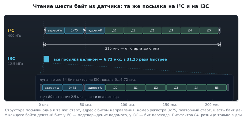
Speed. The structure of a transfer has remained the same: a start, an address byte with the direction bit, then data bytes, each with a ninth bit. Reading six bytes from a sensor register is 84 bit clocks on both I²C and I3C. The difference is only in the clock length: at 400 kHz the transfer takes 210 µs, at 12.5 MHz 6.72 µs, that is 31 times less. There is no other magic in the "speed of I3C".
Addresses are handed out at start-up. Instead of a fixed address each device has a 64-bit business card: a 48-bit factory number plus two bytes describing what kind of device it is and what it can do. The master announces on the bus the address assignment procedure, the devices put out their cards simultaneously — and, since the line is open-drain, the one with the smaller number wins: another device's one is overridden by another device's zero, the loser sees the mismatch and stays silent until the next round. In this way the master goes through all devices in one pass and gives each one a seven-bit address.
Hence a consequence that breaks a habit: the device address is no longer a constant.
If addresses are handed out with the ENTDAA procedure, after a bus restart it may
turn out different, and you cannot "hard-code 0x68 in the driver" — the device is found
by its factory number or by the description from its card. If a device has a
static address, the master can assign it as the dynamic one too (SETDASA,
for all at once SETAASA), and the address stays predictable. But that is decided by the
master, not by the device.
An interrupt inside the bus. When a sensor has something to say, it does not toggle
a separate wire but pulls SDA to zero in a pause and then transmits its
address — by the same "smaller number wins" rule if two speak at once.
The master receives the address and, if the device supports it, one or two bytes explaining
what exactly happened. A microcontroller pin is saved, along with all the code around the
external interrupt (section 7), and the response delay no longer depends on the polling
period: instead of "we poll a hundred times a second and learn on average after 5 ms" —
"we learn at the end of the current transfer", that is within microseconds.
Common commands. Part of the work that in I²C is always specific to each sensor is described by the standard here: allow or forbid a device to speak up and to join on the fly, assign a new address, reset the address assignment, report the maximum read and write length. The commands are the same for all — the bus driver handles them itself, before the conversation with a particular sensor begins.
What it looks like in the STM32 block. The H5 has few registers, and their names show everything listed:
| Register | What for |
|---|---|
CFGR |
who we are on the bus: the master or a target device (CRINIT) |
DEVR0 |
our own address and a flag that the address has been assigned (DAVAL) |
DEVR1…DEVR4 |
the addresses of the devices to which the master assigned them — up to four |
EPIDR |
our own factory number, the very one with which the device introduces itself |
BCR, DCR |
the two bytes of the card: what kind of device and what it can do |
IBIDR |
the explanation bytes that arrived together with the device's signal |
EVR |
event flags, among them "a device spoke up" (IBIF) |
TIMINGR0…TIMINGR2 |
durations: the clock, the pauses, the times for switching to the push-pull output |
Old I²C devices live on the same bus: the master starts the conversation with the
reserved address 0x7E, to which they do not respond, and if there are no old
devices on the bus, this header is disabled with the NOARBH bit in CFGR — for the sake of
those nine bit clocks.
⚠️ Three traps when switching over. The first: the pull-ups. A push-pull output and kilo-ohm resistors mean extra current and degraded edges; on an I3C bus a single weak resistor is fitted, and only for the open-drain phases. The second: there is no clock stretching — a slow slave that on I²C simply held
SCLsilently loses data here. The third: the address is dynamic, see above.Terms used in the documentation
Term Meaning controller / target the master / the target device dynamic address assignment ( ENTDAA)handing out addresses at bus start-up provisioned ID ( EPIDR)the device's factory number bus / device characteristics register ( BCR,DCR)the card bytes: bus properties and device type in-band interrupt ( IBI)an interrupt inside the bus hot-join joining the bus on the fly common command code ( CCC)a command that is the same for all devices arbitration header ( 0x7E)the header that cuts off old I²C devices push-pull / open-drain an output that drives both levels / one that only pulls low transition bit ( T)the ninth bit of a transfer instead of ACK
17.12 Pitfalls
No pull-ups. The bus does not work at all.
The pins are configured as push-pull. A conflict with the slave.
The address format is mixed up. 0x68 versus 0xD0.
ADDR was not fully cleared. Only SR1 was read.
No timeouts. A wire that came off hangs the program forever.
Too many devices with their own pull-ups. The parallel resistors give too low a total resistance.
400 kHz does not start on a long cable. At 400 pF the pull-up must be no higher than 885 Ω, but the usual 4.7 kΩ are fitted — a 1.6 µs edge instead of 300 ns. Switching to 100 kHz does not save you: there too the limit is 1000 ns, and 4.7 kΩ gives 1.6 µs. Either a lower resistor (for 400 kHz no more than 885 Ω, for 100 kHz no more than 2.95 kΩ), or shorter wires.
Long wires. The line capacitance stretches the edges, TRISE no longer
matches reality. Half a metre at 400 kHz is already a lot.
A common ground is forgotten. A sensor on a separate board must have a common ground with the microcontroller, otherwise the levels are meaningless.
The EEPROM loses part of what was written. The write crossed a page boundary, and the address wrapped around to the start of the page.
A read right after a write to the EEPROM gets a refusal. A write cycle of up to 5 ms is in progress. Readiness must be polled.
The 24C08 writes to the wrong place. A 16-bit cell address is selected, and the second byte of the address became data.
A counter in the EEPROM "died" after two weeks. It was written once a second, while the endurance is a million cycles.
PEC corrupted a sensor register. The SMBus checksum was sent to an ordinary I²C device.
17.13 Summary
- Both pins are open-drain, pull-up resistors are mandatory: 4.7 kΩ for 100 kHz, 2.2 kΩ for 400 kHz.
CR2.FREQis the APB1 bus frequency, not the I²C speed; the speed is set byCCR.- The address is seven bits and is put shifted left; the lowest bit is the direction.
- The
ADDRflag is cleared by readingSR1, thenSR2— otherwise the bus is stuck. - When reading a single byte the acknowledge is removed before clearing
ADDR. - All flag waits in production code — only with timeouts.
- The peripheral has documented defects, including the busy flag getting stuck: read the errata in advance.
- A stuck bus is revived with nine
SCLclocks by hand and a software reset of the block. - A 24C EEPROM is written by pages, polling readiness after each: the write cycle is up to 5 ms. On the 24C04…24C16 the upper bits of the cell address go into the device address, and the cell address itself is eight bits. The endurance is a million cycles.
- SMBus 2.0 is I²C with restrictions: from 10 to 100 kHz,
SCLlow for no longer than 35 ms, fixed levels of 0.8 and 2.1 V, a PEC checksum — CRC-8; SMBus 3.0 added 400 kHz and 1 MHz and lowered the upper threshold to 1.35 V.
Full sources
i2c_f0.c — the new-style I²C on the STM32F072: reading a sensor register.
/* Раздел 17.10: I²C нового образца на STM32F072 — I2C1 на PB6/PB7 (AF1), такт HSI 8 МГц,
 * 100 кГц через TIMINGR; чтение регистра датчика. */
#include <stddef.h>
#include "stm32f0xx.h"

_Static_assert(offsetof(I2C_TypeDef, TIMINGR) == 0x10u, "TIMINGR вместо CR2.FREQ, CCR и TRISE");
_Static_assert(offsetof(I2C_TypeDef, ISR) == 0x18u && offsetof(I2C_TypeDef, ICR) == 0x1Cu, "ISR/ICR вместо SR1/SR2");
_Static_assert(offsetof(I2C_TypeDef, RXDR) == 0x24u && offsetof(I2C_TypeDef, TXDR) == 0x28u, "два регистра данных");

/* Такт I2C1 у F0 после сброса — HSI 8 МГц (RCC_CFGR3_I2C1SW = 0).
 * PRESC = 1: шаг 2 / 8 МГц = 250 нс; SCLL = 19 -> низкий уровень 20 шагов = 5,0 мкс,
 * SCLH = 15 -> высокий 16 шагов = 4,0 мкс; SDADEL 2, SCLDEL 4 — задержки данных. */
#define I2C_HZ  8000000u
#define PRESC   1u
#define SCLL    19u
#define SCLH    15u
#define SDADEL  2u
#define SCLDEL  4u
#define T_STEP_NS ((PRESC + 1u) * 1000000u / (I2C_HZ / 1000u))
_Static_assert(T_STEP_NS == 250u, "шаг 250 нс");
_Static_assert((SCLL + 1u) * T_STEP_NS == 5000u && (SCLH + 1u) * T_STEP_NS == 4000u, "5,0 и 4,0 мкс");
#define TIMING ((PRESC << I2C_TIMINGR_PRESC_Pos) | (SCLDEL << I2C_TIMINGR_SCLDEL_Pos) \
              | (SDADEL << I2C_TIMINGR_SDADEL_Pos) | (SCLH << I2C_TIMINGR_SCLH_Pos) | (SCLL << I2C_TIMINGR_SCLL_Pos))
_Static_assert(TIMING == 0x10420F13u, "TIMINGR для 100 кГц от 8 МГц");

void i2c1_init_f0(void)
{
    RCC->AHBENR |= RCC_AHBENR_GPIOBEN;
    RCC->APB1ENR |= RCC_APB1ENR_I2C1EN;
    GPIOB->OTYPER |= (1u << 6) | (1u << 7);                          /* открытый сток */
    GPIOB->AFR[0] = (GPIOB->AFR[0] & ~(0xFu << 24) & ~(0xFu << 28)) | (1u << 24) | (1u << 28);   /* AF1 */
    GPIOB->MODER = (GPIOB->MODER & ~(3u << 12) & ~(3u << 14)) | (2u << 12) | (2u << 14);
    I2C1->CR1 &= ~I2C_CR1_PE;
    I2C1->TIMINGR = TIMING;                     /* одно число вместо FREQ, CCR и TRISE */
    I2C1->CR1 |= I2C_CR1_PE;
}

uint8_t i2c1_read_reg_f0(uint8_t addr7, uint8_t reg, uint8_t *value)
{
    /* 1. Адрес, один байт на запись, без STOP — дальше повторный старт. */
    I2C1->CR2 = ((uint32_t)addr7 << 1) | (1u << I2C_CR2_NBYTES_Pos) | I2C_CR2_START;
    while (!(I2C1->ISR & (I2C_ISR_TXIS | I2C_ISR_NACKF))) {
    }
    if (I2C1->ISR & I2C_ISR_NACKF) {            /* никто не ответил на адрес */
        I2C1->ICR = I2C_ICR_NACKCF;
        return 1u;
    }
    I2C1->TXDR = reg;
    while (!(I2C1->ISR & I2C_ISR_TC)) {         /* байт ушёл, STOP не выдан */
    }
    /* 2. Повторный старт, один байт на чтение; STOP блок выдаст сам — AUTOEND. */
    I2C1->CR2 = ((uint32_t)addr7 << 1) | I2C_CR2_RD_WRN | (1u << I2C_CR2_NBYTES_Pos)
              | I2C_CR2_AUTOEND | I2C_CR2_START;
    while (!(I2C1->ISR & I2C_ISR_RXNE)) {
    }
    *value = (uint8_t)I2C1->RXDR;
    while (!(I2C1->ISR & I2C_ISR_STOPF)) {
    }
    I2C1->ICR = I2C_ICR_STOPCF;
    return 0u;
}
i2c_g0.c — the same I²C on the STM32G071.
/* Раздел 17.10: тот же I²C на STM32G071 — I2C1 на PB6/PB7 (AF6), такт PCLK 64 МГц. */
#include <stddef.h>
#include "stm32g0xx.h"

_Static_assert(offsetof(I2C_TypeDef, TIMINGR) == 0x10u && offsetof(I2C_TypeDef, TXDR) == 0x28u,
               "блок тот же, что у F0");

/* Такт I2C1 у G0 после сброса — PCLK (RCC_CCIPR_I2C1SEL = 0), 64 МГц.
 * Тот же шаг 250 нс: PRESC = 15 -> 16 / 64 МГц; остальные поля — как у F0. */
#define I2C_HZ  64000000u
#define PRESC   15u
#define SCLL    19u
#define SCLH    15u
#define SDADEL  2u
#define SCLDEL  4u
#define T_STEP_NS ((PRESC + 1u) * 1000000u / (I2C_HZ / 1000u))
_Static_assert(T_STEP_NS == 250u, "шаг 250 нс");
#define TIMING ((PRESC << I2C_TIMINGR_PRESC_Pos) | (SCLDEL << I2C_TIMINGR_SCLDEL_Pos) \
              | (SDADEL << I2C_TIMINGR_SDADEL_Pos) | (SCLH << I2C_TIMINGR_SCLH_Pos) | (SCLL << I2C_TIMINGR_SCLL_Pos))
_Static_assert(TIMING == 0xF0420F13u, "TIMINGR для 100 кГц от 64 МГц");

void i2c1_init_g0(void)
{
    RCC->IOPENR |= RCC_IOPENR_GPIOBEN;
    RCC->APBENR1 |= RCC_APBENR1_I2C1EN;                              /* у G0 — APBENR1 */
    GPIOB->OTYPER |= (1u << 6) | (1u << 7);
    GPIOB->AFR[0] = (GPIOB->AFR[0] & ~(0xFu << 24) & ~(0xFu << 28)) | (6u << 24) | (6u << 28);   /* AF6 */
    GPIOB->MODER = (GPIOB->MODER & ~(3u << 12) & ~(3u << 14)) | (2u << 12) | (2u << 14);
    I2C1->CR1 &= ~I2C_CR1_PE;
    I2C1->TIMINGR = TIMING;
    I2C1->CR1 |= I2C_CR1_PE;
}

/* Обмен — слово в слово как у F0: тот же CR2, те же флаги. */
uint8_t i2c1_read_reg_g0(uint8_t addr7, uint8_t reg, uint8_t *value)
{
    I2C1->CR2 = ((uint32_t)addr7 << 1) | (1u << I2C_CR2_NBYTES_Pos) | I2C_CR2_START;
    while (!(I2C1->ISR & (I2C_ISR_TXIS | I2C_ISR_NACKF))) {
    }
    if (I2C1->ISR & I2C_ISR_NACKF) {
        I2C1->ICR = I2C_ICR_NACKCF;
        return 1u;
    }
    I2C1->TXDR = reg;
    while (!(I2C1->ISR & I2C_ISR_TC)) {
    }
    I2C1->CR2 = ((uint32_t)addr7 << 1) | I2C_CR2_RD_WRN | (1u << I2C_CR2_NBYTES_Pos)
              | I2C_CR2_AUTOEND | I2C_CR2_START;
    while (!(I2C1->ISR & I2C_ISR_RXNE)) {
    }
    *value = (uint8_t)I2C1->RXDR;
    while (!(I2C1->ISR & I2C_ISR_STOPF)) {
    }
    I2C1->ICR = I2C_ICR_STOPCF;
    return 0u;
}
Next: section 17а "The microcontroller as a slave device: I²C and SPI".