 Embedded HandbookApps
19а. CAN FD on FDCAN: 64 bytes, two bit rates, message RAM
Classic CAN from section 19 transfers no more than 8 bytes per frame and no faster than 1 Mbit/s. CAN FD removes both limits: up to 64 bytes per frame and a second, fast bit rate while the data is being transferred. Arbitration (who has priority on the bus) runs at the same old slow rate — that is why the wires and transceivers stay almost the same.
The newer STM32 series (G4, H7, L5, U5) have an FDCAN module instead of bxCAN. This section is about it, using the G4 as the example: length codes, the two bit rates and how to calculate them, transceiver delay compensation, the message RAM and the operating modes.
The module is described from the G4 reference manual; the memory layout was
also cross-checked against the constants of the HAL driver from the same package. Everything that
is calculated was calculated by the program _verify/can19a/canfd.c (gcc on the computer).
It is checked by _verify/can19a_check.py.
Terms used in the documentation
Term Meaning FDF (FD format) the flag marking a CAN FD frame BRS (bit rate switch) switching the bit rate inside a frame ESI (error state indicator) the flag "the transmitter is error passive" nominal / data bit timing the bit timing of the arbitration phase and of the data phase time quantum (tq) the time quantum sample point the moment the bit value is read transmitter delay compensation (TDC), secondary sample point (SSP) delay compensation and the second sample point message RAM the memory that holds the frames restricted operation mode a restricted mode: receive and acknowledge only
19а.1 What changed in the frame
- The bit that was reserved in the classic frame became FDF: recessive — a CAN FD frame, dominant — a classic one.
- It is followed by res and BRS: with BRS recessive, the bit rate inside the frame switches to the fast one.
- ESI — the transmitter reports whether it is in the error passive state.
- DLC 0…8 means the same as before; codes 9…15 are lengths beyond 8:
| DLC | 0…8 | 9 | 10 | 11 | 12 | 13 | 14 | 15 |
|---|---|---|---|---|---|---|---|---|
| bytes | 0…8 | 12 | 16 | 20 | 24 | 32 | 48 | 64 |
An arbitrary length cannot be sent: 9 bytes go out in a frame of 12 (DLC 9), 33 bytes — in a frame of 48 (DLC 14), and the rest is padded. The program picks the smallest suitable code:
| Bytes needed | DLC | Sent | Extra |
|---|---|---|---|
| 9 | 9 | 12 | 3 |
| 13 | 10 | 16 | 3 |
| 33 | 14 | 48 | 15 |
| 49 | 15 | 64 | 15 |
CAN FD is enabled with the FDOE bit, bit rate switching with BRSE (both in CCCR;
they can be changed only with INIT = 1 and CCE = 1). The module always receives and
transmits classic frames.
These bits only allow. What kind of frame goes out is decided by the header of the transmit
element: the FDF (FD frame) and BRS (fast phase) bits in the second word,
next to the DLC. In HAL these are the header fields FDFormat = FDCAN_FD_CAN and
BitRateSwitch = FDCAN_BRS_ON. Forget them, and with FDOE = 1 a classic
frame goes out, no longer than 8 bytes.
19а.2 Two bit rates: how to calculate them
The bit time is a whole number of quanta: 1 synchronization quantum + the segment before
the sample point + the segment after it. For the arbitration phase these are fields of the NBTP register,
for the data phase — DBTP; each is stored "minus one":
| Field | Range in the register | Meaning |
|---|---|---|
| NBRP / DBRP | 0…511 / 0…31 | divider of the CAN kernel clock → quantum |
| NTSEG1 / DTSEG1 | 0…255 / 0…31 | before the sample point |
| NTSEG2 / DTSEG2 | 0…127 / 0…15 | after the sample point |
| NSJW / DSJW | 0…127 / 0…15 | resynchronization limit; DSJW is less than DTSEG2 |
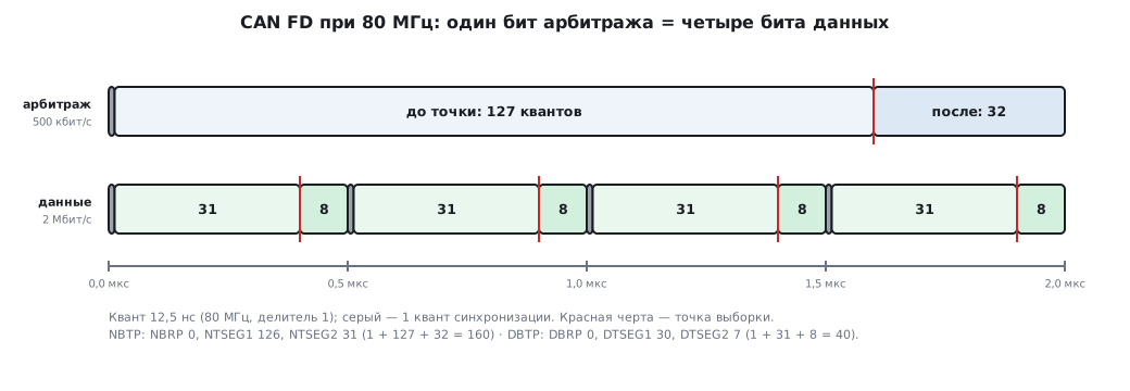
The program searches for dividers for a CAN kernel clock of 80 MHz and a sample point of 80 %:
| Phase | Rate | Divider | Quanta per bit | Before the point | After | Point | Into the register |
|---|---|---|---|---|---|---|---|
| arbitration | 500 kbit/s | 1 | 160 | 127 | 32 | 80 % | NBRP 0, NTSEG1 126, NTSEG2 31 |
| data | 2 Mbit/s | 1 | 40 | 31 | 8 | 80 % | DBRP 0, DTSEG1 30, DTSEG2 7 |
| data | 5 Mbit/s | 1 | 16 | 12 | 3 | 81.2 % | — |
| data | 8 Mbit/s | 1 | 10 | 7 | 2 | 80 % | — |
A bit cannot be shorter than 4 quanta; the manual's example — a 20 MHz kernel clock and a bit of 4 quanta give 5 Mbit/s in the data phase. The faster the CAN kernel clock, the more quanta per bit and the more precisely the sample point can be placed.
Where to get 80 MHz. On the G4 the CAN kernel clock is selected with the FDCANSEL field
in RCC_CCIPR: the HSE crystal (the reset default), the Q output of the PLL or PCLK1;
it is then divided by the divider in FDCAN_CKDIV, common to all modules. The Q output
gives 80 MHz with SYSCLK at 160 MHz: the PLL at 320 MHz, dividers R = 2 and Q = 4.
At 170 MHz the PLL runs at 340 MHz, and the Q output gives 85 MHz: for 2 Mbit/s that is
42.5 quanta, which does not divide evenly. Then you take PCLK1 = 170 MHz — divider 5
and 17 quanta per bit. In any case the source is a crystal: the frequency of the internal
HSI16 drifts with temperature by 1…2 %, while CAN FD nodes at megabit rates
may differ by only tenths of a percent.
A catch in the documentation. The general description in the chapter gives the segments as "from 1 to 16" and "from 1 to 8 quanta" — that was the old bxCAN. The FDCAN register fields are wider (up to 256 and 128 in the arbitration phase); calculate from the field descriptions.
All nodes of the network must match in both bit rates and in the sample point: with different sample points at a high rate, the nodes read the bit at different moments.
19а.3 Transceiver delay
In the data phase the transmitter compares what went out with what came back through the transceiver. The echo lags by the transceiver delay, and at the fast rate this is already a noticeable fraction of a bit: without correction the transmitter "sees" an error where there is none. That is why, without compensation, the data phase bit rate is limited by the transceiver delay.
Compensation (TDC) is enabled with the TDC bit in DBTP. The module itself measures
the delay on every FD frame — from the falling edge between FDF and res to the same edge at
the RX input — and compares the bits at the secondary sample point: the measured delay
plus the offset TDCO. It is usually set equal to the position of the sample point
of the data phase in CAN kernel clock cycles: at 80 MHz and 2 Mbit/s — about 32 cycles,
80 % of the bit. Limitations:
- the delay plus
TDCOmust be less than 6 bits of the data phase; - and no more than 127 minimum quanta (CAN kernel clock cycles); anything larger is taken as 127;
TDCFsets a window that keeps a short glitch from ending the measurement too early.
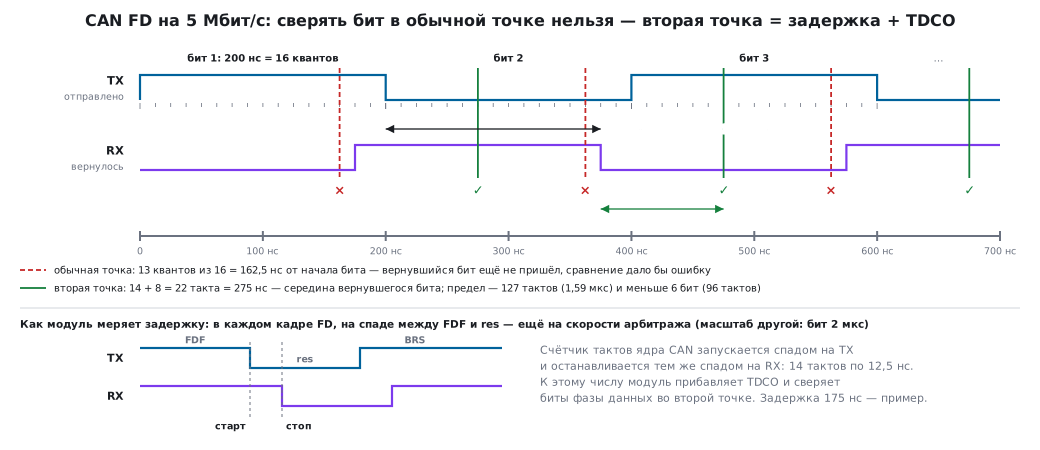
In the arbitration phase compensation is always off — there the long bit covers the delay.
19а.4 Message RAM
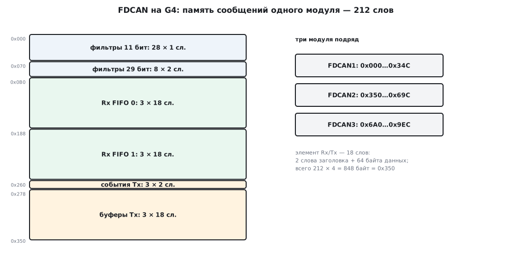
FDCAN stores frames not in registers but in a separate message RAM. On the G4 its layout is fixed: up to 212 words of 32 bits per module, and the sections are always the same. The program calculated them from the element sizes:
| Section | Elements | Words per element | Start |
|---|---|---|---|
| filters for 11-bit identifiers | 28 | 1 | 0x000 |
| filters for 29-bit ones | 8 | 2 | 0x070 |
| Rx FIFO 0 | 3 | 18 | 0x0B0 |
| Rx FIFO 1 | 3 | 18 | 0x188 |
| Tx events | 3 | 2 | 0x260 |
| Tx buffers | 3 | 18 | 0x278 |
| total | 0x350 = 848 bytes = 212 words |
A receive or transmit element is 18 words: 2 header words (identifier, DLC, flags, timestamp) and 16 words = 64 bytes of data — there is always room for the longest frame.
The modules follow one another: FDCAN1 from 0x000, FDCAN2 from 0x350, FDCAN3 from 0x6A0 from the start of the common area. The HAL driver calculates it the same way: the module address is the base plus 0x350 × number. In the manual's example for two modules the second one starts at 0x0354 — one word further; here working code deserves more trust than the example.
Three elements per FIFO is not much. The firmware must take frames quickly (in
the interrupt), otherwise the FIFO overflows. What happens then is chosen with the F0OM
and F1OM bits in RXGFC: blocking (the default — new frames are lost)
or overwrite (new ones overwrite old ones).
19а.5 Modes that come in handy
| Mode | How to enable | What for |
|---|---|---|
| restricted (Restricted) | CCCR.ASM |
only receive and acknowledge; detecting the network bit rate — try rates until a correct frame arrives |
| monitoring (Bus monitoring) | CCCR.MON |
listen to the bus without driving anything onto it: an analyzer |
| external loopback | TEST.LBCK |
your own frames are received back; they are visible on the TX pin |
| internal loopback | TEST.LBCK + CCCR.MON |
self-test without affecting a running bus |
| no retransmission (DAR) | CCCR.DAR |
a frame is not retransmitted after losing arbitration or after an error |
For the test modes, first set CCCR.TEST = 1. Restricted mode is also entered
by itself if the module failed to read a frame from the message RAM in time —
you can leave it only by clearing ASM.
The timestamp is a 16-bit counter in CAN bits (prescaler 1…16); it is captured at the start of every received and transmitted frame.
19а.6 Classic and FD nodes on one bus
A node that does not understand CAN FD (or has it disabled), when receiving an FD frame, sends an error frame — and destroys it. That is why you cannot mix them. The manual describes how networks move to FD:
- at startup all nodes talk classic CAN until they are sure that all of them understand FD — then they switch;
- if there are noticeably more errors in the data phase than in arbitration, bit rate switching is turned off;
- wake-up frames of partial networks are classic;
- during programming on the assembly line, nodes without FD are kept in "listen only" mode.
19а.7 Pitfalls
A node raises errors on every FD frame. It has FDOE = 0, or it is
classic — it is supposed to destroy such frames.
FD is enabled, but classic 8-byte frames go out. FDF and BRS are not set in the transmit header
(FDFormat, BitRateSwitch in HAL): FDOE and BRSE
only allow.
The data rate "does not work" at 5 Mbit/s. Transceiver delay compensation is not enabled — the bit comparison falls within the delay.
The sample point "wanders". The CAN kernel clock is such that there are few quanta per bit: at 80 MHz for 8 Mbit/s — only 10.
The bit timing settings are not written. NBTP and DBTP can be written
only with INIT = 1 and CCE = 1.
Sent 9 bytes — received 12. An FD frame length can only be one of 12, 16, 20, 24, 32, 48, 64. The length of the useful data is carried by the data itself.
Frames get lost. Each Rx FIFO has only 3 elements.
The second FDCAN "corrupts" the frames of the first. Its memory address was calculated by hand with an error — FDCAN2 starts at 0x350, not at 0x354.
Entered restricted mode and "went silent". It failed to read the message RAM in time;
the way out is to clear ASM.
19а.8 Summary
- CAN FD: up to 64 bytes; FDF marks the frame, BRS switches the bit rate, ESI signals that the transmitter is error passive. DLC 9…15 → 12, 16, 20, 24, 32, 48, 64.
- Two bit rates — two sets of fields (
NBTP,DBTP), each "minus one". At 80 MHz: 500 kbit/s — 160 quanta, 2 Mbit/s — 40, sample point 80 %. - A bit is at least 4 quanta: 20 MHz → up to 5 Mbit/s.
- A fast data phase requires transceiver delay compensation (
TDC,TDCO). - G4 message RAM: 212 words per module, the layout is fixed; the modules start at 0x000, 0x350, 0x6A0.
- Nodes without FD on the same bus destroy FD frames.
Next: section 19б "CANopen: object dictionary, NMT, PDO and SDO".