 Embedded HandbookApps
44. Analog blocks inside the chip: OPAMP and COMP
Between a sensor and the ADC there is almost always at least one operational amplifier, and next to a power switch there is a comparator that turns PWM off faster than any interrupt. The higher STM32 families have both on the chip: with gain resistors, with a threshold from a built-in DAC, with an output going straight into the ADC or into the timer break input. This section covers what these blocks can do, what they cannot do, and how to build overcurrent protection from them without adding anything to the board but a shunt.
The reference chips here are the G474 (six op-amps, seven comparators) and the L476 (two of each); the F103 and F407 are mentioned as families that lack these blocks, where the task is solved differently.
Terms used in the documentation
Term Meaning operational amplifier (op-amp, OPAMP) operational amplifier comparator (COMP) comparator rail-to-rail input and output work over the whole range from ground to supply input offset voltage zero offset voltage, "the offset" offset trimming, calibration adjusting the offset, calibration gain-bandwidth product (GBW) gain times bandwidth slew rate rate of rise of the output voltage programmable gain amplifier (PGA) amplifier with programmable gain follower, unity-gain buffer follower, buffer with gain 1 common-mode input range range of the voltage common to both inputs hysteresis different thresholds for switching on and off propagation delay time from crossing the threshold to the output change blanking the output is ignored for the duration of a disturbance window comparator two thresholds, an "inside the window" signal break input (BKIN) timer emergency input shunt resistor resistor whose voltage drop is used to measure current internal voltage reference (VREFINT) internal reference voltage
44.1 Who has what
Built-in analog circuitry is a mark of families designed for motor control and power converters. The "classic" families do not have it.
| Family | Op-amps | Comparators | PGA gain | Alternative |
|---|---|---|---|---|
| F103, F407 | — | — | — | an external op-amp; instead of a comparator, the ADC analog watchdog (section 14.8), but that is microseconds, not nanoseconds |
| F303 | 4 | 7 | ×2…×16 | — |
| L476 | 2 | 2 | ×2…×16 | — |
| G431 | 3 | 4 | ×2…×64 | — |
| G474 | 6 | 7 | ×2…×64 | — |
The number of blocks and the register bits below come from the family headers; where the section says "on the G4", both G4 chips are meant — they differ only in the count.
44.2 What the built-in op-amp can do
This is not a precision amplifier from a catalogue but a fast and convenient "good enough" op-amp. You need to know its parameters (G4, typical; limits in parentheses), because they set the limits of where it can be used.
| Parameter | Value | What it means in practice |
|---|---|---|
| offset after calibration | ±1.5 mV at 25 °C (±3 mV over the full range) | input-referred error: at ×16 that is ±24…48 mV at the output |
| offset drift | ±10 µV/°C | 60 °C of heating adds another 0.6 mV |
| bandwidth (GBW) | 13 MHz (at least 7) | divided by the gain: about 0.8 MHz at ×16, 0.2 MHz at ×64 |
| slew rate | 6.5 V/µs; 45 V/µs in high-speed mode | 0 → 3.3 V in 0.5 µs or in 73 ns |
| output | up to 100 mV from each supply rail | rail-to-rail; the top of the scale is VDDA − 0.1 V |
| load current | 500 µA (270 µA in PGA) | load no lower than ≈6.6 kΩ (≈12 kΩ in PGA); capacitance up to 50 pF |
| open-loop gain | 95 dB | — |
| PGA gain accuracy | 1 % (2 % at the extremes: ×2, ×32, ×64) | divider resistors ±15 %, but their ratio holds |
| wake-up | 3 µs | turn it on in advance, not right before a measurement |
| consumption | 1.3 mA (0.45 mA with internal output) | turn it off in sleep modes |
| input current | pin leakage: up to ±100…150 nA — a limit from the pin table, no typical value | a source up to 10 kΩ adds no more than the offset (1.5 mV); 1 MΩ at 100 nA is already 100 mV of error (section 56.4) |
Input and output are rail-to-rail, common-mode range 0…VDDA; there is no negative supply, so only positive signals can be amplified — or they must be shifted to the middle of the scale.
44.3 Four configurations without external parts
Inside there is the amplifier itself plus multiplexers on the inputs and the output and a resistive feedback divider. Configuring the op-amp means configuring the multiplexers.
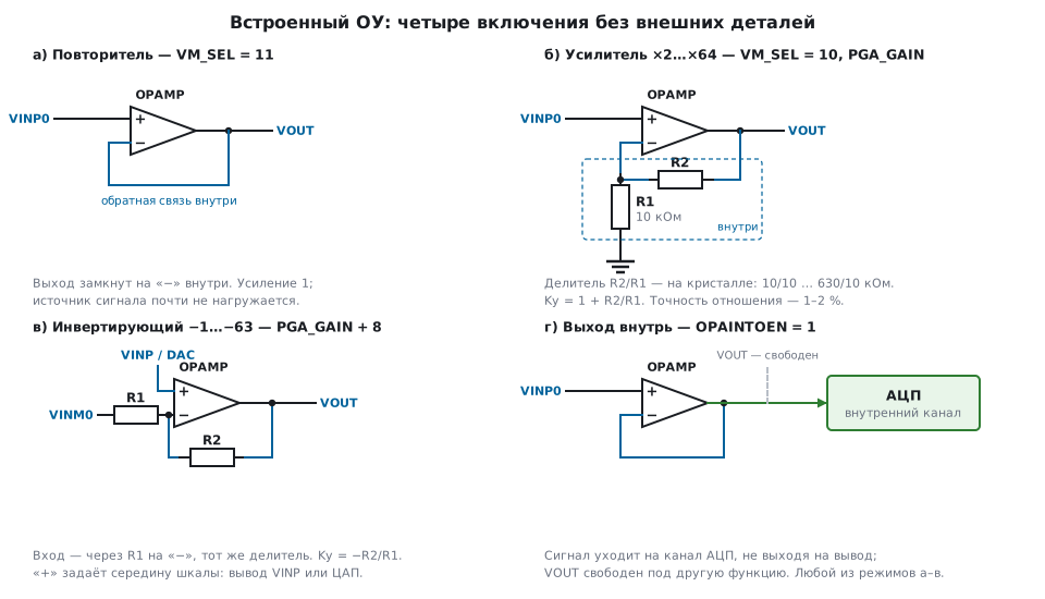
OPAMP_CSR field |
Code | What is connected |
|---|---|---|
VP_SEL ("+" input) |
00 / 01 / 10 | pin VINP0 / VINP1 / VINP2 |
| 11 | a DAC channel (on the second op-amp, a fourth pin) | |
VM_SEL ("−" input) |
00 / 01 | pin VINM0 / VINM1 — external feedback |
| 10 | internal divider — PGA amplifier | |
| 11 | its own output — follower | |
PGA_GAIN |
0…5 | ×2, ×4, ×8, ×16, ×32, ×64 |
| +8 | inverting configuration: input through R1 from pin VINM0, gain −1…−63; or an external bias on VINM0 | |
| +16 | VINM0 is additionally brought out to "−" — for a filter capacitor | |
| +24 | inverting with a filter on VINM1 | |
OPAINTOEN |
1 | output goes inside, to an ADC channel; the VOUT pin is free |
HIGHSPEEDEN |
1 | high-speed mode (45 V/µs, more current) |
The divider is the same for both directions: non-inverting gain
1 + R2/R1 gives ×2…×64, inverting −R2/R1 on the same resistors is
one less: −1…−63.
Follower. The most common configuration: a buffer between a high-impedance source (a megaohm divider, a piezo sensor, a photodiode) and the ADC, which needs a source of a few kilohms (section 14.2).
/* Повторитель: вход VINP0, выход на вывод VOUT.
   ОУ и компараторы G4 тактируются вместе с SYSCFG. */
static void opamp1_follower(void)
{
    RCC->APB2ENR |= RCC_APB2ENR_SYSCFGEN;
    OPAMP1->CSR = (VPSEL_VINP0    << OPAMP_CSR_VPSEL_Pos)
                | (VMSEL_FOLLOWER << OPAMP_CSR_VMSEL_Pos)
                | OPAMP_CSR_OPAMPxEN;
}
×16 amplifier with output to the ADC. Not a single external resistor: the signal from the shunt arrives at VINP0, is amplified and goes to an internal channel.
static void opamp1_pga16_to_adc(void)
{
    RCC->APB2ENR |= RCC_APB2ENR_SYSCFGEN;
    OPAMP1->CSR = (VPSEL_VINP0   << OPAMP_CSR_VPSEL_Pos)
                | (VMSEL_PGA     << OPAMP_CSR_VMSEL_Pos)
                | (PGA_CODE(16u) << OPAMP_CSR_PGGAIN_Pos)
                | OPAMP_CSR_OPAMPINTEN          /* вывод VOUT остаётся свободным */
                | OPAMP_CSR_OPAMPxEN;
}
Where exactly the internal output goes is fixed in the header: OPAMP1 → ADC1, channel 13; OPAMP2 → ADC2, channel 16; OPAMP3 → ADC3, channel 13. When reading this channel, the sampling time must be no shorter than 200 ns (section 14.2).
⚠️ Bandwidth is divided by the gain. ×64 is already 200 kHz, and a current pulse a microsecond long passes through such an amplifier smoothed out. To protect fast switches, use a lower gain and a larger shunt, or put the comparator before the amplifier.
44.4 Offset and trimming it
Offset is the main error of an op-amp, and gain does not cure it — it multiplies it. On a 10 mΩ shunt, an offset of 1.5 mV is 150 mA of current error, 3 mV is 300 mA. That is why the built-in op-amp has two ways of trimming:
- factory — codes written during production, used by
default (
USERTRIM = 0); gives ±1.5 mV at room temperature; - user —
USERTRIM = 1, the codes in theTRIMOFFSETPandTRIMOFFSETNfields (5 bits each, step 1.1…1.65 mV) are found by the firmware itself at the current temperature.
There are two trims because the input stage is dual: one works at
low common-mode voltage, the other at high. Each is calibrated at
its own voltage: CALSEL applies 3.3 / 10 / 50 / 90 % of VDDA to the inputs.
Procedure: enable calibration (CALON), select the voltage, increase the
code from zero and wait for settling after each step; the first code at
which the OUTCAL bit changes from 1 to 0 is the one you want.
extern void delay_ms(uint32_t ms);

static uint32_t trim_scan(uint32_t calsel, uint32_t pos, uint32_t msk)
{
    uint32_t code;
    OPAMP1->CSR = (OPAMP1->CSR & ~OPAMP_CSR_CALSEL_Msk) | (calsel << OPAMP_CSR_CALSEL_Pos);
    for (code = 0u; code < 32u; code++) {
        OPAMP1->CSR = (OPAMP1->CSR & ~msk) | (code << pos);
        delay_ms(2u);
        if ((OPAMP1->CSR & OPAMP_CSR_OUTCAL) == 0u)
            break;                                  /* первый код, при котором выход упал */
    }
    return code;
}

static void opamp1_user_calibrate(void)
{
    uint32_t work = OPAMP1->CSR;                    /* рабочая настройка — вернуть потом */
    OPAMP1->CSR = OPAMP_CSR_USERTRIM | OPAMP_CSR_CALON | OPAMP_CSR_OPAMPxEN;
    (void)trim_scan(CALSEL_90, OPAMP_CSR_TRIMOFFSETN_Pos, OPAMP_CSR_TRIMOFFSETN_Msk);
    (void)trim_scan(CALSEL_10, OPAMP_CSR_TRIMOFFSETP_Pos, OPAMP_CSR_TRIMOFFSETP_Msk);
    OPAMP1->CSR = (work & ~(OPAMP_CSR_TRIMOFFSETP_Msk | OPAMP_CSR_TRIMOFFSETN_Msk | OPAMP_CSR_CALON))
                | (OPAMP1->CSR & (OPAMP_CSR_TRIMOFFSETP_Msk | OPAMP_CSR_TRIMOFFSETN_Msk))
                | OPAMP_CSR_USERTRIM;
}
The library function HAL_OPAMP_SelfCalibrate() does the same with a binary
search and a 2 ms pause per step. Calibrate at start-up, once the chip
has warmed up to operating temperature, and repeat if the temperature changes
noticeably: a drift of 10 µV/°C over 60 °C eats 0.6 mV.
The LOCK bit freezes CSR until reset: a protection setting that a stray
write cannot spoil.
44.5 Internal output, timer-controlled switching, DAC buffer
Into the ADC without a pin. OPAINTOEN = 1 disconnects the output from the pin and
feeds it to an internal ADC channel. You save a pin, there is no pickup
on the trace, and consumption drops to 0.45 mA.
Switching inputs on a timer event. The OPAMP_TCMR register sets
a second set of inputs (VPS_SEL, VMS_SEL) and allows switching between the sets
on signals from TIM1, TIM8 or TIM20 (T1CM_EN, T8CM_EN, T20CM_EN). This way
one op-amp serves two shunts of two motors: in the first half of the PWM
period it amplifies the current of one, in the second the other, and the ADC picks up both.
DAC buffer. The "+" input with code 11 takes a DAC channel, and on the G4 that is DAC3 or
DAC4 (except for the second op-amp, which gets a fourth pin): these DACs have no
pins of their own, and the follower brings them out — that is the main point.
The dead zones near the rails are smaller than with the DAC's own buffer
(0.2 V, section 15.3), but they do not disappear: the op-amp output does not reach the rails by
0.1 V (table 44.2), and the load must be no lower than ≈6.6 kΩ. For fast
signals, use the high-speed mode HIGHSPEEDEN.
44.6 The comparator: structure and parameters
A comparator is an op-amp without feedback and with a digital output: "+" above "−" gives one, below gives zero. Its strength is time: it does not convert, it compares.
| Parameter (G4) | Value | Note |
|---|---|---|
| delay | 17 ns typical, 31 ns maximum (VDDA ≥ 2.7 V) | interrupt entry at 170 MHz takes 71 ns: the comparator is faster than the jump to the handler itself |
| offset | −6/+2 mV (no worse than −9/+3) | worse than the op-amp's — set the threshold with a margin |
| hysteresis | 0…70 mV, 8 steps | code × 10 mV nominal; typical ≈ 9 mV × code, spread up to a factor of two |
| consumption | 450 µA | plus 1 µA for the reference divider |
| start-up | 5 µs | the VREFINT divider takes up to 200 µs |
The inputs are set by COMP_CSR fields:
| Field | Code | Source |
|---|---|---|
INPSEL ("+", signal) |
0 / 1 | first or second INP pin |
INMSEL ("−", threshold) |
0 / 1 / 2 / 3 | ¼ / ½ / ¾ / 1 × VREFINT (1.212 V): 0.303 / 0.606 / 0.909 / 1.212 V |
| 4 / 5 | two DAC channels (for COMP1, DAC3_CH1 and DAC1_CH1) | |
| 6 / 7 | two INM pins | |
SCALEN, BRGEN |
1 | reference buffer and the ¼ ½ ¾ divider — enable together with codes 0…3 |
POLARITY |
1 | invert the output |
HYST |
0…7 | hysteresis |
BLANKING |
0…7 | whose pulse blanks the output (for example, TIM1 OC5) |
LOCK |
1 | freeze until reset |
VALUE |
— | current output state (read) |
Hysteresis is a must for a noisy analog signal: without it the output chatters near the threshold, and a timer in break mode catches every bounce. 20 mV at the comparator input with ×16 gain and a 10 mΩ shunt is a 125 mA current "dead zone".
Blanking. At the moment the power switch toggles there is a spike on the shunt — capacitive, not a real current. The comparator will see it. Blanking feeds the comparator a pulse from a timer channel (TIM1 OC5, tied to the switching moment), and for the duration of the pulse the output does not change. The threshold stays the same, and false trips disappear.
DAC as the threshold. The G4 has DACs without pins — DAC3 and DAC4 — exactly for this: their output goes only inside, to the comparators and op-amps. The protection threshold becomes a number in a register and can be changed on the fly.
44.7 Where the comparator output goes
Four destinations, any of them at the same time:
| Where | How to enable | Why |
|---|---|---|
| to a pin | GPIO alternate function | an external driver, an oscilloscope |
| to EXTI (lines 21, 22, 29…33 on the G4) | EXTI_IMR1, edge in RTSR1/FTSR1; lines 32 and 33 (COMP6, COMP7) in EXTI_IMR2, RTSR2/FTSR2 |
interrupt; wake-up from Stop (section 10.6) — the comparator works without clocks |
| to the TIM1/TIM8/TIM20 break input | TIMx_AF1: bit BKCMPnE |
PWM is switched off in hardware, within tens of nanoseconds, without the core (section 13.5) |
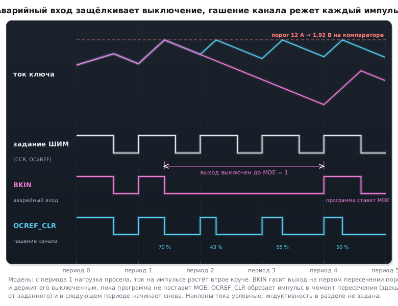
| to channel clearing (OCREF_CLR) | TIMx_AF2.OCRSEL = comparator number, SMCR.OCCS = 0, CCMRx.OCxCE = 1 |
the channel is turned off until the end of the current period and turns on again in the next: cycle-by-cycle current limiting |
The difference between the last two: the break input is a latch, the timer output stays off until the software intervenes; channel clearing is a limiter that acts in every period and needs no handling at all.
/* Ограничение тока внутри периода: COMP1 гасит канал 1 TIM1 до следующего периода. */
static void tim1_ch1_clear_by_comp1(void)
{
    TIM1->AF2   = (TIM1->AF2 & ~TIM1_AF2_OCRSEL_Msk) | (0u << TIM1_AF2_OCRSEL_Pos);  /* 0 — COMP1 */
    TIM1->SMCR &= ~TIM_SMCR_OCCS;                   /* источник гашения — внутренний, не ETR */
    TIM1->CCMR1 |= TIM_CCMR1_OC1CE;                 /* разрешить гашение канала 1 */
}
The seven comparators of the G474 share three interrupt vectors: COMP1_2_3,
COMP4_5_6, COMP7; in the handler the source is identified by the EXTI line
flags.
44.8 🔧 Overcurrent protection entirely inside the chip
The task: a switch drives a load of up to 10 A; at 12 A the PWM must be turned off faster than the switch can burn out, and the current must be measured for regulation.
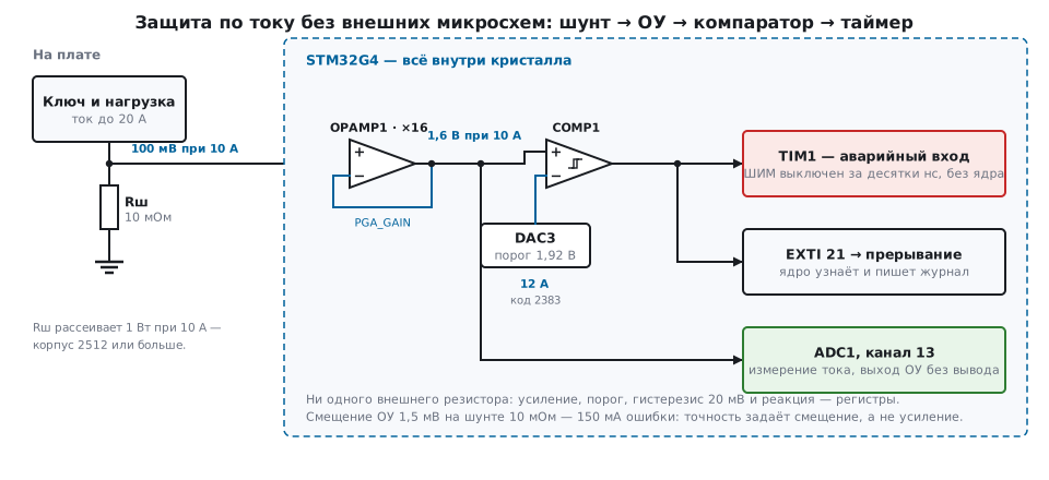
Calculation:
- 10 mΩ shunt: at 10 A that is 100 mV, dissipating 1 W (a 2512 package or larger);
- op-amp ×16: 1.6 V at nominal current; the upper measurement limit is output saturation at VDDA − 0.1 V, that is 20 A;
- threshold 12 A → 120 mV → 1.92 V at the comparator; the 12-bit DAC code at VDDA 3.3 V: 1.92 / 3.3 × 4095 = 2383;
- errors: op-amp offset 1.5 mV ≡ 150 mA, gain 2 % ≡ 200 mA at 10 A; hysteresis 20 mV ≡ 125 mA. A 12 A threshold at a nominal 10 A accommodates these errors.
static void comp1_overcurrent(uint16_t dac_code)
{
    RCC->AHB2ENR |= RCC_AHB2ENR_DAC3EN | RCC_AHB2ENR_ADC12EN;
    RCC->APB2ENR |= RCC_APB2ENR_SYSCFGEN | RCC_APB2ENR_TIM1EN;

    DAC3->MCR     = (DAC_MODE_INTERNAL_NOBUF << DAC_MCR_MODE1_Pos)  /* выход только внутрь */
                  | DAC_MCR_HFSEL_1;                                /* AHB 170 МГц: режим «выше 160 МГц» */
    DAC3->DHR12R1 = dac_code;                       /* порог */
    DAC3->CR     |= DAC_CR_EN1;

    COMP1->CSR = (INM_DAC_A      << COMP_CSR_INMSEL_Pos)    /* «−» — порог из DAC3_CH1 */
               | (0u             << 8)                      /* «+» — первый вывод INP */
               | (HYST_20MV      << COMP_CSR_HYST_Pos)
               | (BLANK_TIM1_OC5 << COMP_CSR_BLANKING_Pos)
               | COMP_CSR_EN;

    /* Выход компаратора — на аварийный вход TIM1: ШИМ гаснет без участия ядра. */
    TIM1->AF1  |= TIM1_AF1_BKCMP1E;
    TIM1->BDTR |= TIM_BDTR_BKP | TIM_BDTR_BKE;    /* авария — единицей: компаратор выдаёт 1 при перегрузке */

    /* И на EXTI 21 — чтобы ядро узнало и записало событие. */
    EXTI->IMR1  |= EXTI_IMR1_IM21;
    EXTI->RTSR1 |= EXTI_RTSR1_RT21;
    NVIC_EnableIRQ(COMP1_2_3_IRQn);
}

/* Настройку защиты — заморозить до сброса. */
static void analog_lock(void)
{
    COMP1->CSR  |= COMP_CSR_LOCK;
    OPAMP1->CSR |= OPAMP_CSR_LOCK;
}
Check the polarity separately. After reset BKP = 0: the break input
trips on zero, and the comparator output reaches it through that same
polarity (each comparator also has its own inversion bit BKCMPnP
in AF1). But the comparator here outputs zero in normal operation — without BKP = 1 the break
would be active all the time, and the PWM would never start at all. The other way is to
invert the comparator output with the POLARITY bit or the timer input with the
BKCMP1P bit.
Call order: amplifier (opamp1_pga16_to_adc), calibration, threshold
and comparator, then LOCK. The op-amp signal simultaneously goes to channel 13 of
ADC1 — the controller reads the current with an ordinary scan with DMA (section 14.6),
while the protection lives separately and does not depend on the software.
What matters here: between the shunt and the PWM being switched off there is not a single processor instruction. The comparator takes 17 ns, the timer break input is a hardware latch. The interrupt is only needed for logging.
44.9 Differences on L4 and F3
L476. Two op-amps and two comparators, simpler in design:
- the mode is the
OPAMODEfield (0 — external feedback, 2 — PGA, 3 — follower), gainPGA_GAINin two bits: ×2…×16; - low-power mode
OPALPM— less current, narrower bandwidth; the trim for it is stored separately (registersOTRandLPOTR); OPA_RANGE= 1 when VDDA ≥ 2.4 V — you must set it, otherwise the amplifier works outside its range;- the clock is a separate bit
OPAMPENinAPB1ENR1, not SYSCFG; - the comparator has three speeds (
PWRMODE: fast / medium / low-power), four hysteresis steps and a window mode (WINMODE): the "+" of the second comparator is taken from the first, two thresholds — and an "inside / outside the window" signal without the core.
static void opamp1_follower_l4(void)
{
    RCC->APB1ENR1 |= RCC_APB1ENR1_OPAMPEN;
    OPAMP1->CSR = (OPAMODE_FOLLOWER << OPAMP1_CSR_OPAMODE_Pos)
                | OPAMP1_CSR_OPARANGE                /* питание 3,3 В — «высокий» диапазон */
                | OPAMP1_CSR_OPAEN;
}
F303. The op-amp is the direct ancestor of the G4: the same CSR layout, gain
only ×2…×16. The comparator chooses its output destination itself, with the OUTSEL field
in its own register; on the G4 it is the other way round — the timer chooses the comparator in AF1.
44.10 HAL
| Function | What it does |
|---|---|
HAL_OPAMP_Init / DeInit |
mode, inputs, gain, speed, trimming — from the Init structure |
HAL_OPAMP_Start / Stop |
OPAEN |
HAL_OPAMP_SelfCalibrate, HAL_OPAMPEx_SelfCalibrateAll |
trimming one or all op-amps (2 ms per step) |
HAL_OPAMP_Lock |
LOCK |
HAL_COMP_Init / DeInit |
inputs, threshold, hysteresis, polarity, blanking; on some families also the EXTI edge |
HAL_COMP_Start / Stop (on some families Start_IT) |
enabling, with an interrupt if needed |
HAL_COMP_GetOutputLevel |
current output state |
HAL_COMP_TriggerCallback |
callback from the EXTI handler |
HAL_COMP_Lock |
LOCK |
HAL does not set up the link between the comparator and the timer — that is done in the
timer initialisation (BreakInputSource, OCREF_CLR) or directly
in AF1/AF2.
44.11 Pitfalls
The op-amp "does not work". The clock is not enabled: on G4 and F3 it is SYSCFGEN,
on L4 OPAMPEN. Or the pin is not set to analog mode.
The ×64 amplifier "smooths" the signal. Bandwidth 13 MHz / 64 = 200 kHz. Lower gain, larger shunt.
Readings drift with heating. Factory trimming is done at 25 °C, drift is 10 µV/°C. Calibrate at operating temperature and repeat.
The output "hits a wall" at 3.2 V. Saturation 100 mV below the rail: the top of the scale is VDDA − 0.1 V; plan the gain for it.
The op-amp drives 1 kΩ and the voltage sags. Drive capability is 500 µA: minimum ≈6.6 kΩ, ≈12 kΩ in PGA.
The first measurement after enabling is garbage. Wake-up is 3 µs; turn the op-amp on in advance, not right before the ADC sample.
The comparator chatters. No hysteresis, or the noise is larger than it. Set
HYST, and for PWM spikes use blanking from the timer.
The threshold from VREFINT "floats" for the first milliseconds. The reference divider
takes up to 200 µs to start — enable SCALEN/BRGEN in advance and wait.
The comparator trips, but the PWM does not turn off. The output is not linked to the timer:
on G4, the BKCMPnE bit in AF1 and BKE in BDTR; on F3, OUTSEL in the
comparator itself.
The PWM does not start: a break right after enabling. The break input
polarity after reset is zero (BKP = 0), and the comparator outputs zero in normal
operation. Set BKP = 1 or invert the comparator output.
The protection settings changed by themselves. No LOCK; after it only a
reset can change them.
The DAC threshold at 170 MHz behaves unpredictably. HFSEL is not set
in DAC_MCR: with an AHB frequency above 80 MHz it is mandatory (01 — above 80,
10 — above 160 MHz) and gives the transfer of the code to the DAC output extra bus cycles.
HAL sets it itself based on the bus frequency; register-level code does so only if you do not
forget.
After Stop the comparator does not wake the chip. The comparator's EXTI line is not unmasked (21…33 on the G4), or no edge is selected.
L4: the amplifier behaves strangely. OPA_RANGE does not match VDDA.
44.12 Summary
- Built-in op-amps and comparators exist on F3, L4, G4; F1 and F4 do not have them — use an external op-amp and the ADC analog watchdog there.
- Op-amp: rail-to-rail, 13 MHz, ×2…×64 on the internal divider, offset ±1.5 mV after calibration; the error is set by the offset, not by the gain.
- Four configurations are four multiplexer codes: follower, PGA, inverting, internal output to the ADC.
- Calibration is two 5-bit codes, found using the
OUTCALbit; repeat it when the temperature changes. - Comparator: 17 ns, hysteresis up to 70 mV, threshold from fractions of VREFINT, a DAC without pins, or a pin; blanking cuts off switching spikes.
- The comparator output goes to a pin, to EXTI (including wake-up from Stop), to the timer break input and to channel clearing.
- Overcurrent protection is built without a single external resistor except
the shunt and does not depend on the software;
LOCKprotects it from the software itself.
Next: section 45 "Touch input: TSC" — capacitive buttons and sliders without mechanical parts.