 Embedded HandbookПриложения
Приложение A16. Карты регистров STM32U5
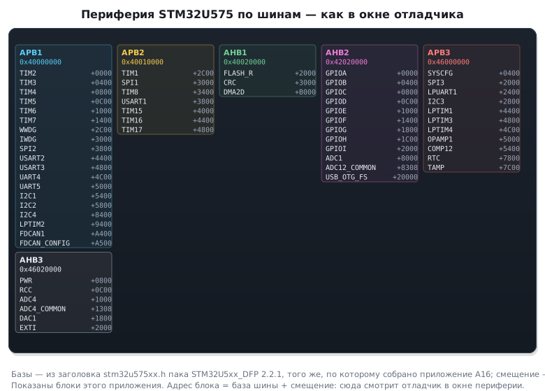
Серия STM32U5: Cortex-M33 до 160 МГц — наименьшее потребление среди быстрых серий. Регистры и биты основных блоков — из заголовка STM32U575, тем же генератором, что карты F1 и F4: смещения — по структурам *_TypeDef, назначение регистра и описание бита — из комментариев заголовка. Блоки, которых в серии нет, опущены. Для малого потребления смотрите PWR (режимы сна), RCC (генераторы LSE/LSI/MSI), LPTIM и LPUART — они работают во сне. Разделы справочника написаны для F103 и F407; имена регистров и битов у серий в основном те же — карта помогает перенести код и увидеть, что устроено иначе.
Как читать: смещение — от базового адреса блока; 31:16 — поле битов
с 16 по 31; одно число — отдельный бит. Цифра в скобках у заголовка
блока — раздел, где блок разобран.
RCC — Тактирование (раздел 6)
| Регистр | Смещение | Бит | Назначение |
|---|---|---|---|
CR |
0x00 |
32 | RCC clock control register |
RCC_CR_MSISON |
0 | Internal Multi Speed Oscillator (MSIS) Clock Enable | |
RCC_CR_MSIKERON |
1 | MSI Enable for Some IPs Kernels | |
RCC_CR_MSISRDY |
2 | Internal Multi Speed Oscillator (MSIS) Clock Ready Flag | |
RCC_CR_MSIPLLEN |
3 | Internal Multi Speed Oscillator (MSI) PLL Mode Enable | |
RCC_CR_MSIKON |
4 | Internal Multi Speed Oscillator Kernel (MSIK) Enable | |
RCC_CR_MSIKRDY |
5 | Internal Multi Speed Oscillator Kernel (MSIK) Ready Flag | |
RCC_CR_MSIPLLSEL |
6 | Internal Multi Speed Oscillator (MSI) PLL Mode Selection | |
RCC_CR_MSIPLLFAST |
7 | Internal Multi Speed Oscillator (MSI) PLL Fast Mode Selection | |
RCC_CR_HSION |
8 | Internal High Speed Oscillator (HSI16) Clock Enable | |
RCC_CR_HSIKERON |
9 | Internal High Speed Oscillator (HSI16) Clock Enable for some IPs Kernel | |
RCC_CR_HSIRDY |
10 | Internal High Speed Oscillator (HSI16) Clock Ready Flag | |
RCC_CR_HSI48ON |
12 | Internal High Speed Oscillator (HSI48) Clock Enable | |
RCC_CR_HSI48RDY |
13 | Internal High Speed Oscillator (HSI48) Clock Ready Flag | |
RCC_CR_SHSION |
14 | Internal High Speed Secure (SHSI) Clock Enable | |
RCC_CR_SHSIRDY |
15 | Internal High Speed Secure (SHSI) Clock Ready Flag | |
RCC_CR_HSEON |
16 | External High Speed Oscillator (HSE) Clock Enable | |
RCC_CR_HSERDY |
17 | External High Speed Oscillator (HSE) Clock Ready | |
RCC_CR_HSEBYP |
18 | External High Speed Oscillator (HSE) Clock Bypass | |
RCC_CR_CSSON |
19 | HSE Clock Security System Enable | |
RCC_CR_HSEEXT |
20 | External High Speed clock type in Bypass Mode | |
RCC_CR_PLL1ON |
24 | System PLL 1 Clock Enable | |
RCC_CR_PLL1RDY |
25 | System PLL 1 Clock Ready Flag | |
RCC_CR_PLL2ON |
26 | System PLL 2 Enable | |
RCC_CR_PLL2RDY |
27 | System PLL 2 Ready Flag | |
RCC_CR_PLL3ON |
28 | System PLL 3 Enable | |
RCC_CR_PLL3RDY |
29 | System PLL 3 Ready Flag | |
ICSCR1 |
0x08 |
32 | RCC internal clock sources calibration register 1 |
RCC_ICSCR1_MSICAL3 |
0:4 | MSICAL[4:0] bits: MSIRC3 Clock Calibration for MSI Ranges 12 to 15 | |
RCC_ICSCR1_MSIRGSEL |
3 | Internal Multi Speed oscillator (MSI) range selection | |
RCC_ICSCR1_MSICAL2 |
5:9 | MSICAL[4:0] bits: MSIRC2 Clock Calibration for MSI Ranges 8 to 11 | |
RCC_ICSCR1_MSICAL1 |
10:14 | MSICAL[4:0] bits: MSIRC1 Clock Calibration for MSI Ranges 4 to 7 | |
RCC_ICSCR1_MSICAL0 |
15:19 | MSICAL[4:0] bits: MSIRC0 Clock Calibration for MSI Ranges 0 to 3 | |
RCC_ICSCR1_MSIBIAS |
22 | Internal Multi Speed oscillator (MSI) BIAS mode selection | |
RCC_ICSCR1_MSIKRANGE |
24:27 | Internal Multi Speed oscillator Kernel (MSIK) clock Ranges | |
RCC_ICSCR1_MSISRANGE |
28:31 | Internal Multi Speed oscillator (MSI) clock Ranges | |
ICSCR2 |
0x0C |
32 | RCC internal clock sources calibration register 2 |
RCC_ICSCR2_MSITRIM3 |
0:4 | MSITRIM[4:0] bits: MSI Clock Trimming for Ranges 12 to 15 | |
RCC_ICSCR2_MSITRIM2 |
5:9 | MSITRIM[4:0] bits: MSI Clock Trimming for Ranges 8 to 11 | |
RCC_ICSCR2_MSITRIM1 |
10:14 | MSITRIM[4:0] bits: MSI Clock Trimming for Ranges 4 to 7 | |
RCC_ICSCR2_MSITRIM0 |
15:19 | MSITRIM[4:0] bits: MSI Clock Trimming for Ranges 0 to 3 | |
ICSCR3 |
0x10 |
32 | RCC internal clock sources calibration register 3 |
RCC_ICSCR3_HSICAL |
0:11 | HSICAL[11:0] bits: HSI Clock Calibration | |
RCC_ICSCR3_HSITRIM |
24:30 | HSITRIM[4:0] bits: HSI Clock Trimming | |
CRRCR |
0x14 |
32 | RCC Clock Recovery RC Register |
RCC_CRRCR_HSI48CAL |
0:8 | HSI48CAL[4:0] bits: HSI48 Clock Calibration | |
CFGR1 |
0x1C |
32 | RCC clock configuration register 1 |
RCC_CFGR1_SW |
0:1 | SW[1:0] bits (System clock Switch) | |
RCC_CFGR1_SWS |
2:3 | SWS[1:0] bits (System Clock Switch Status) | |
RCC_CFGR1_STOPWUCK |
15 | Wake Up from stop and CSS backup clock selection | |
RCC_CFGR1_STOPKERWUCK |
15 | Kernel Clock Selection after a Wake Up from STOP | |
RCC_CFGR1_MCOSEL |
24:27 | MCOSEL [3:0] bits (Microcontroller Clock Output (MCO) Selection) | |
RCC_CFGR1_MCOPRE |
28:30 | MCOPRE [2:0] bits (Microcontroller Clock Output (MCO) Prescaler) | |
CFGR2 |
0x20 |
32 | RCC clock configuration register 2 |
RCC_CFGR2_HPRE |
0:3 | HPRE[3:0] bits (AHB prescaler) | |
RCC_CFGR2_PPRE1 |
4:6 | PPRE1[2:0] bits (APB1 prescaler) | |
RCC_CFGR2_PPRE2 |
8:11 | PPRE2[2:0] bits (APB2 prescaler) | |
RCC_CFGR2_AHB1DIS |
16 | AHB1 clock disable | |
RCC_CFGR2_AHB2DIS1 |
17 | AHB2 clock disable | |
RCC_CFGR2_AHB2DIS2 |
18 | AHB2 clock disable | |
RCC_CFGR2_APB1DIS |
19 | APB1 clock disable | |
RCC_CFGR2_APB2DIS |
20 | APB2 clock disable | |
CFGR3 |
0x24 |
32 | RCC clock configuration register 3 |
RCC_CFGR3_PPRE3 |
4:6 | PPRE31[2:0] bits (APB3 prescaler) | |
RCC_CFGR3_AHB3DIS |
16 | AHB3 clock disable | |
RCC_CFGR3_APB3DIS |
17 | APB3 clock disable | |
PLL1CFGR |
0x28 |
32 | PLL1 Configuration Register |
RCC_PLL1CFGR_PLL1SRC |
0:1 | PLL1SRC[1:0] bits (PLL1 Entry Clock Source) | |
RCC_PLL1CFGR_PLL1RGE |
2:3 | PLL1RGE[1:0] bits (PLL1 Input Frequency Range) | |
RCC_PLL1CFGR_PLL1FRACEN |
4 | PLL1 Fractional Latch Enable | |
RCC_PLL1CFGR_PLL1M |
4:9 | PLL1M[3:0]: bits (Prescaler for PLL1) | |
RCC_PLL1CFGR_PLL1MBOOST |
4:9 | PLL1MBOOST[3:0]: bits (Prescaler for EPOD booster input clock) | |
RCC_PLL1CFGR_PLL1PEN |
16 | PLL1 DIVP Divider Output Enable | |
RCC_PLL1CFGR_PLL1QEN |
17 | PLL1 DIVQ Divider Output Enable | |
RCC_PLL1CFGR_PLL1REN |
18 | PLL1 DIVR Divider Output Enable | |
PLL2CFGR |
0x2C |
32 | PLL2 Configuration Register |
RCC_PLL2CFGR_PLL2SRC |
0:1 | PLL2SRC[1:0] bits (PLL2 Entry Clock Source) | |
RCC_PLL2CFGR_PLL2RGE |
2:3 | PLL2RGE[1:0] bits (PLL2 Input Frequency Range) | |
RCC_PLL2CFGR_PLL2FRACEN |
4 | PLL2 Fractional Latch Enable | |
RCC_PLL2CFGR_PLL2M |
4:9 | PLL2M[3:0]: bits (Prescaler for PLL2) | |
RCC_PLL2CFGR_PLL2PEN |
16 | PLL2 DIVP Divider Output Enable | |
RCC_PLL2CFGR_PLL2QEN |
17 | PLL2 DIVQ Divider Output Enable | |
RCC_PLL2CFGR_PLL2REN |
18 | PLL2 DIVR Divider Output Enable | |
PLL3CFGR |
0x30 |
32 | PLL3 Configuration Register |
RCC_PLL3CFGR_PLL3SRC |
0:1 | PLL3SRC[1:0] bits (PLL3 Entry Clock Source) | |
RCC_PLL3CFGR_PLL3RGE |
2:3 | PLL3RGE[1:0] bits (PLL3 Input Frequency Range) | |
RCC_PLL3CFGR_PLL3FRACEN |
4 | PLL3 Fractional Latch Enable | |
RCC_PLL3CFGR_PLL3M |
4:9 | PLL3M[3:0]: bits (Prescaler for PLL3) | |
RCC_PLL3CFGR_PLL3PEN |
16 | PLL3 DIVP Divider Output Enable | |
RCC_PLL3CFGR_PLL3QEN |
17 | PLL3 DIVQ Divider Output Enable | |
RCC_PLL3CFGR_PLL3REN |
18 | PLL3 DIVR Divider Output Enable | |
PLL1DIVR |
0x34 |
32 | PLL1 Dividers Configuration Register |
RCC_PLL1DIVR_PLL1N |
0:8 | PLL1N[8:0]: bits (Multiplication Factor For PLL1 VCO) | |
RCC_PLL1DIVR_PLL1P |
9:15 | PLL1P[6:0]: bits (PLL1 DIVP Division Factor) | |
RCC_PLL1DIVR_PLL1Q |
16:22 | PLL1Q[6:0]: bits (PLL1 DIVQ Division Factor) | |
RCC_PLL1DIVR_PLL1R |
24:30 | PLL1R[6:0]: bits (PLL1 DIVR Division Factor) | |
PLL1FRACR |
0x38 |
32 | PLL1 Fractional Divider Configuration Register |
RCC_PLL1FRACR_PLL1FRACN |
3:15 | PLL1FRACN[12:0]: bits (Fractional Part of the Multiplication Factor for PLL1 VCO) | |
PLL2DIVR |
0x3C |
32 | PLL2 Dividers Configuration Register |
RCC_PLL2DIVR_PLL2N |
0:8 | PLL2N[8:0]: bits (Multiplication Factor for PLL2 VCO) | |
RCC_PLL2DIVR_PLL2P |
9:15 | PLL2P[6:0]: bits (PLL2 DIVP Division Factor) | |
RCC_PLL2DIVR_PLL2Q |
16:22 | PLL2Q[6:0]: bits (PLL2 DIVQ Division Factor) | |
RCC_PLL2DIVR_PLL2R |
24:30 | PLL2R[6:0]: bits (PLL2 DIVR Division Factor) | |
PLL2FRACR |
0x40 |
32 | PLL2 Fractional Divider Configuration Register |
RCC_PLL2FRACR_PLL2FRACN |
3:15 | PLL2FRACN[12:0]: bits (Fractional Part of the Multiplication Factor for PLL2 VCO) | |
PLL3DIVR |
0x44 |
32 | PLL3 Dividers Configuration Register |
RCC_PLL3DIVR_PLL3N |
0:8 | PLL3N[8:0]: bits (Multiplication Factor for PLL3 VCO) | |
RCC_PLL3DIVR_PLL3P |
9:15 | PLL3P[6:0]: bits (PLL2 DIVP Division Factor) | |
RCC_PLL3DIVR_PLL3Q |
16:22 | PLL3Q[6:0]: bits (PLL3 DIVQ Division Factor) | |
RCC_PLL3DIVR_PLL3R |
24:30 | PLL3R[6:0]: bits (PLL3 DIVR Division Factor) | |
PLL3FRACR |
0x48 |
32 | PLL3 Fractional Divider Configuration Register |
RCC_PLL3FRACR_PLL3FRACN |
3:15 | PLL3FRACN[12:0]: bits (Fractional Part of the Multiplication Factor for PLL3 VCO) | |
CIER |
0x50 |
32 | Clock Interrupt Enable Register |
RCC_CIER_LSIRDYIE |
0 | LSI Ready Interrupt Enable | |
RCC_CIER_LSERDYIE |
1 | LSE Ready Interrupt Enable | |
RCC_CIER_MSISRDYIE |
2 | MSIS Ready Interrupt Enable | |
RCC_CIER_HSIRDYIE |
3 | HSI16 Ready Interrupt Enable | |
RCC_CIER_HSERDYIE |
4 | HSE Ready Interrupt Enable | |
RCC_CIER_HSI48RDYIE |
5 | HSI48 Ready Interrupt Enable | |
RCC_CIER_PLL1RDYIE |
6 | PLL Ready Interrupt Enable | |
RCC_CIER_PLL2RDYIE |
7 | PLL2 Ready Interrupt Enable | |
RCC_CIER_MSIKRDYIE |
7 | MSIK Ready Interrupt Enable | |
RCC_CIER_PLL3RDYIE |
8 | PLL3 Ready Interrupt Enable | |
RCC_CIER_SHSIRDYIE |
8 | SHSI Ready Interrupt Enable | |
CIFR |
0x54 |
32 | Clock Interrupt Flag Register |
RCC_CIFR_LSIRDYF |
0 | LSI Ready Interrupt Flag | |
RCC_CIFR_LSERDYF |
1 | LSE Ready Interrupt Flag | |
RCC_CIFR_MSISRDYF |
2 | MSIS Ready Interrupt Flag | |
RCC_CIFR_HSIRDYF |
3 | HSI16 Ready Interrupt Flag | |
RCC_CIFR_HSERDYF |
4 | HSE Ready Interrupt Flag | |
RCC_CIFR_HSI48RDYF |
5 | HSI48 Ready Interrupt Flag | |
RCC_CIFR_PLL1RDYF |
6 | PLL1 Ready Interrupt Flag | |
RCC_CIFR_PLL2RDYF |
7 | PLL2 Ready Interrupt Flag | |
RCC_CIFR_MSIKRDYF |
7 | MSIK Ready Interrupt Flag | |
RCC_CIFR_PLL3RDYF |
8 | PLL3 Ready Interrupt Flag | |
RCC_CIFR_SHSIRDYF |
8 | SHSI Ready Interrupt Flag | |
RCC_CIFR_CSSF |
10 | Clock Security System Interrupt Flag | |
CICR |
0x58 |
32 | Clock Interrupt Clear Register |
RCC_CICR_LSIRDYC |
0 | LSI Ready Interrupt Clear | |
RCC_CICR_LSERDYC |
1 | LSE Ready Interrupt Clear | |
RCC_CICR_MSISRDYC |
2 | MSIS Ready Interrupt Clear | |
RCC_CICR_HSIRDYC |
3 | HSI16 Ready Interrupt Clear | |
RCC_CICR_HSERDYC |
4 | HSE Ready Interrupt Clear | |
RCC_CICR_HSI48RDYC |
5 | HSI48 Ready Interrupt Clear | |
RCC_CICR_PLL1RDYC |
6 | PLL1 Ready Interrupt Clear | |
RCC_CICR_PLL2RDYC |
7 | PLL2 Ready Interrupt Clear | |
RCC_CICR_MSIKRDYC |
7 | MSIK Ready Interrupt Clear | |
RCC_CICR_PLL3RDYC |
8 | PLL3 Ready Interrupt Clear | |
RCC_CICR_SHSIRDYC |
8 | SHSI Ready Interrupt Clear | |
RCC_CICR_CSSC |
10 | Clock Security System Interrupt Clear | |
AHB1RSTR |
0x60 |
32 | AHB1 Peripherals Reset Register |
RCC_AHB1RSTR_GPDMA1RST |
0 | GPDMA1 Reset | |
RCC_AHB1RSTR_CORDICRST |
1 | CORDIC Reset | |
RCC_AHB1RSTR_FMACRST |
2 | FMAC Reset | |
RCC_AHB1RSTR_MDF1RST |
3 | MDF1 Reset | |
RCC_AHB1RSTR_CRCRST |
12 | CRC Reset | |
RCC_AHB1RSTR_TSCRST |
16 | TSC Reset | |
RCC_AHB1RSTR_RAMCFGRST |
17 | RAMCFG Reset | |
RCC_AHB1RSTR_DMA2DRST |
18 | DMA2D Reset | |
AHB2RSTR1 |
0x64 |
32 | AHB2 Peripherals Reset Register 1 |
RCC_AHB2RSTR1_GPIOARST |
0 | IO port A Reset | |
RCC_AHB2RSTR1_GPIOBRST |
1 | IO port B Reset | |
RCC_AHB2RSTR1_GPIOCRST |
2 | IO port C Reset | |
RCC_AHB2RSTR1_GPIODRST |
3 | IO port D Reset | |
RCC_AHB2RSTR1_GPIOERST |
4 | IO port E Reset | |
RCC_AHB2RSTR1_GPIOFRST |
5 | IO port F Reset | |
RCC_AHB2RSTR1_GPIOGRST |
6 | IO port G Reset | |
RCC_AHB2RSTR1_GPIOHRST |
7 | IO port H Reset | |
RCC_AHB2RSTR1_GPIOIRST |
8 | IO port I Reset | |
RCC_AHB2RSTR1_ADC12RST |
10 | ADC1 Reset | |
RCC_AHB2RSTR1_DCMI_PSSIRST |
12 | DCMI and PSSI Reset | |
RCC_AHB2RSTR1_OTGRST |
14 | OTG Reset | |
RCC_AHB2RSTR1_HASHRST |
17 | Hash Reset | |
RCC_AHB2RSTR1_RNGRST |
18 | Random Number Generator Reset | |
RCC_AHB2RSTR1_OCTOSPIMRST |
21 | OCTOSPIM Reset | |
RCC_AHB2RSTR1_SDMMC1RST |
27 | SDMMC1 Reset | |
RCC_AHB2RSTR1_SDMMC2RST |
27 | SDMMC2 Reset | |
AHB2RSTR2 |
0x68 |
32 | AHB2 Peripherals Reset Register 2 |
RCC_AHB2RSTR2_FSMCRST |
0 | Flexible Memory Controller Reset | |
RCC_AHB2RSTR2_OCTOSPI1RST |
4 | OCTOSPI1 Reset | |
RCC_AHB2RSTR2_OCTOSPI2RST |
8 | OCTOSPI2 Reset | |
AHB3RSTR |
0x6C |
32 | AHB3 Peripherals Reset Register |
RCC_AHB3RSTR_LPGPIO1RST |
0 | LPGPIO1 Reset | |
RCC_AHB3RSTR_ADC4RST |
6 | ADC4 Reset | |
RCC_AHB3RSTR_DAC1RST |
6 | DAC1 Reset | |
RCC_AHB3RSTR_LPDMA1RST |
7 | LPDMA1 Reset | |
RCC_AHB3RSTR_ADF1RST |
10 | ADF1 Reset | |
APB1RSTR1 |
0x74 |
32 | APB1 Peripherals Reset Register 1 |
RCC_APB1RSTR1_TIM2RST |
0 | TIM2 Reset | |
RCC_APB1RSTR1_TIM3RST |
1 | TIM3 Reset | |
RCC_APB1RSTR1_TIM4RST |
2 | TIM4 Reset | |
RCC_APB1RSTR1_TIM5RST |
3 | TIM5 Reset | |
RCC_APB1RSTR1_TIM6RST |
4 | TIM6 Reset | |
RCC_APB1RSTR1_TIM7RST |
5 | TIM7 Reset | |
RCC_APB1RSTR1_SPI2RST |
14 | SPI2 Reset | |
RCC_APB1RSTR1_USART2RST |
17 | USART2 Reset | |
RCC_APB1RSTR1_USART3RST |
18 | USART3 Reset | |
RCC_APB1RSTR1_UART4RST |
19 | UART4 Reset | |
RCC_APB1RSTR1_UART5RST |
20 | UART5 Reset | |
RCC_APB1RSTR1_I2C1RST |
21 | I2C1 Reset | |
RCC_APB1RSTR1_I2C2RST |
22 | I2C2 Reset | |
RCC_APB1RSTR1_CRSRST |
24 | CRS Reset | |
APB1RSTR2 |
0x78 |
32 | APB1 Peripherals Reset Register 2 |
RCC_APB1RSTR2_I2C4RST |
1 | I2C4 Reset | |
RCC_APB1RSTR2_LPTIM2RST |
5 | LPTIM2 Reset | |
RCC_APB1RSTR2_FDCAN1RST |
9 | FDCAN1 Reset | |
RCC_APB1RSTR2_UCPD1RST |
23 | UCPD1 Reset | |
APB2RSTR |
0x7C |
32 | APB2 Peripherals Reset Register |
RCC_APB2RSTR_TIM1RST |
11 | TIM1 Reset | |
RCC_APB2RSTR_SPI1RST |
12 | SPI1 Reset | |
RCC_APB2RSTR_TIM8RST |
13 | TIM8 Reset | |
RCC_APB2RSTR_USART1RST |
14 | USART1 Reset | |
RCC_APB2RSTR_TIM15RST |
16 | TIM15 Reset | |
RCC_APB2RSTR_TIM16RST |
17 | TIM16 Reset | |
RCC_APB2RSTR_TIM17RST |
18 | TIM17 Reset | |
RCC_APB2RSTR_SAI1RST |
21 | SAI1 Reset | |
RCC_APB2RSTR_SAI2RST |
22 | SAI2 Reset | |
APB3RSTR |
0x80 |
32 | APB3 Peripherals Reset Register |
RCC_APB3RSTR_SYSCFGRST |
1 | SYSCFG Reset | |
RCC_APB3RSTR_SPI3RST |
5 | SPI3 Reset | |
RCC_APB3RSTR_LPUART1RST |
6 | LPUART1 Reset | |
RCC_APB3RSTR_I2C3RST |
7 | I2C3 Reset | |
RCC_APB3RSTR_LPTIM1RST |
11 | LPTIM1 Reset | |
RCC_APB3RSTR_LPTIM3RST |
12 | LPTIM3 Reset | |
RCC_APB3RSTR_LPTIM4RST |
13 | LPTIM4 Reset | |
RCC_APB3RSTR_OPAMPRST |
14 | OPAMP Reset | |
RCC_APB3RSTR_COMPRST |
15 | COMP Reset | |
RCC_APB3RSTR_VREFRST |
20 | VREFBUF Reset | |
AHB1ENR |
0x88 |
32 | AHB1 Peripherals Clock Enable Register |
RCC_AHB1ENR_GPDMA1EN |
0 | GPDMA1 Clock Enable | |
RCC_AHB1ENR_CORDICEN |
0 | CORDIC Clock Enable | |
RCC_AHB1ENR_FMACEN |
0 | FMAC Clock Enable | |
RCC_AHB1ENR_MDF1EN |
3 | MDF1 Clock Enable | |
RCC_AHB1ENR_FLASHEN |
8 | FLASH Clock Enable | |
RCC_AHB1ENR_CRCEN |
12 | CRC Clock Enable | |
RCC_AHB1ENR_TSCEN |
16 | Touch Sensing Controller Clock Enable | |
RCC_AHB1ENR_RAMCFGEN |
17 | RAMCFG Clock Enable | |
RCC_AHB1ENR_DMA2DEN |
18 | DMA2D Clock Enable | |
RCC_AHB1ENR_GTZC1EN |
24 | GTZC1 Clock Enable | |
RCC_AHB1ENR_BKPSRAMEN |
28 | BKPSRAM Clock Enable | |
RCC_AHB1ENR_DCACHE1EN |
30 | DCACHE1 Clock Enable | |
RCC_AHB1ENR_SRAM1EN |
31 | SRAM1 Clock Enable | |
AHB2ENR1 |
0x8C |
32 | AHB2 Peripherals Clock Enable Register 1 |
RCC_AHB2ENR1_GPIOAEN |
0 | IO port A Clock Enable | |
RCC_AHB2ENR1_GPIOBEN |
1 | IO port B Clock Enable | |
RCC_AHB2ENR1_GPIOCEN |
2 | IO port C Clock Enable | |
RCC_AHB2ENR1_GPIODEN |
3 | IO port D Clock Enable | |
RCC_AHB2ENR1_GPIOEEN |
4 | IO port E Clock Enable | |
RCC_AHB2ENR1_GPIOFEN |
5 | IO port F Clock Enable | |
RCC_AHB2ENR1_GPIOGEN |
6 | IO port G Clock Enable | |
RCC_AHB2ENR1_GPIOHEN |
7 | IO port H Clock Enable | |
RCC_AHB2ENR1_GPIOIEN |
8 | IO port I Clock Enable | |
RCC_AHB2ENR1_ADC12EN |
10 | ADC1 Clock Enable | |
RCC_AHB2ENR1_DCMI_PSSIEN |
12 | DCMI and PSSI Clock Enable | |
RCC_AHB2ENR1_OTGEN |
14 | OTG Clock Enable | |
RCC_AHB2ENR1_HASHEN |
17 | HASH Clock Enable | |
RCC_AHB2ENR1_RNGEN |
18 | RNG Clock Enable | |
RCC_AHB2ENR1_OCTOSPIMEN |
21 | OCTOSPIM Clock Enable | |
RCC_AHB2ENR1_SDMMC1EN |
27 | SDMMC1 Clock Enable | |
RCC_AHB2ENR1_SDMMC2EN |
28 | SDMMC2 Clock Enable | |
RCC_AHB2ENR1_SRAM2EN |
30 | SRAM2 Clock Enable | |
RCC_AHB2ENR1_SRAM3EN |
31 | SRAM3 Clock Enable | |
AHB2ENR2 |
0x90 |
32 | AHB2 Peripherals Clock Enable Register 2 |
RCC_AHB2ENR2_FSMCEN |
0 | FSMC Clock Enable | |
RCC_AHB2ENR2_OCTOSPI1EN |
4 | OCTOSPI1 Clock Enable | |
RCC_AHB2ENR2_OCTOSPI2EN |
8 | OCTOSPI2 Clock Enable | |
AHB3ENR |
0x94 |
32 | AHB3 Peripherals Clock Enable Register |
RCC_AHB3ENR_LPGPIO1EN |
0 | LPGPIO1 Enable | |
RCC_AHB3ENR_PWREN |
2 | PWR Clock Enable | |
RCC_AHB3ENR_ADC4EN |
6 | ADC4 Clock Enable | |
RCC_AHB3ENR_DAC1EN |
6 | DAC1 Clock Enable | |
RCC_AHB3ENR_LPDMA1EN |
7 | LPDMA1 Clock Enable | |
RCC_AHB3ENR_ADF1EN |
10 | ADF1 Clock Enable | |
RCC_AHB3ENR_GTZC2EN |
12 | GTZC2 Clock Enable | |
RCC_AHB3ENR_SRAM4EN |
35 | SRAM4 Clock Enable | |
APB1ENR1 |
0x9C |
32 | APB1 Peripherals Clock Enable Register 1 |
RCC_APB1ENR1_TIM2EN |
0 | TIM2 Clock Enable | |
RCC_APB1ENR1_TIM3EN |
1 | TIM3 Clock Enable | |
RCC_APB1ENR1_TIM4EN |
2 | TIM4 Clock Enable | |
RCC_APB1ENR1_TIM5EN |
3 | TIM5 Clock Enable | |
RCC_APB1ENR1_TIM6EN |
4 | TIM6 Clock Enable | |
RCC_APB1ENR1_TIM7EN |
5 | TIM7 Clock Enable | |
RCC_APB1ENR1_WWDGEN |
11 | WWDG Clock Enable | |
RCC_APB1ENR1_SPI2EN |
14 | SPI2 Clock Enable | |
RCC_APB1ENR1_USART2EN |
17 | USART2 Clock Enable | |
RCC_APB1ENR1_USART3EN |
18 | USART3 Clock Enable | |
RCC_APB1ENR1_UART4EN |
19 | UART4 Clock Enable | |
RCC_APB1ENR1_UART5EN |
20 | UART5 Clock Enable | |
RCC_APB1ENR1_I2C1EN |
21 | I2C1 Clock Enable | |
RCC_APB1ENR1_I2C2EN |
22 | I2C2 Clock Enable | |
RCC_APB1ENR1_CRSEN |
24 | CRS Clock Enable | |
APB1ENR2 |
0xA0 |
32 | APB1 Peripherals Clock Enable Register 2 |
RCC_APB1ENR2_I2C4EN |
1 | I2C4 Clock Enable | |
RCC_APB1ENR2_LPTIM2EN |
5 | LPTIM2 Clock Enable | |
RCC_APB1ENR2_FDCAN1EN |
9 | FDCAN1 Clock Enable | |
RCC_APB1ENR2_UCPD1EN |
23 | UCPD1 Clock Enable | |
APB2ENR |
0xA4 |
32 | APB2 Peripherals Clock Enable Register |
RCC_APB2ENR_TIM1EN |
11 | TIM1 Clock Enable | |
RCC_APB2ENR_SPI1EN |
12 | SPI1 Clock Enable | |
RCC_APB2ENR_TIM8EN |
13 | TIM8 Clock Enable | |
RCC_APB2ENR_USART1EN |
14 | USART1 Clock Enable | |
RCC_APB2ENR_TIM15EN |
16 | TIM15 Clock Enable | |
RCC_APB2ENR_TIM16EN |
17 | TIM16 Clock Enable | |
RCC_APB2ENR_TIM17EN |
18 | TIM17 Clock Enable | |
RCC_APB2ENR_SAI1EN |
21 | SAI1 Clock Enable | |
RCC_APB2ENR_SAI2EN |
22 | SAI2 Clock Enable | |
APB3ENR |
0xA8 |
32 | APB3 Peripherals Clock Enable Register |
RCC_APB3ENR_SYSCFGEN |
1 | SYSCFG Clock Enable | |
RCC_APB3ENR_SPI3EN |
4 | SPI3 Clock Enable | |
RCC_APB3ENR_LPUART1EN |
6 | LPUART1 Clock Enable | |
RCC_APB3ENR_I2C3EN |
7 | I2C3 Clock Enable | |
RCC_APB3ENR_LPTIM1EN |
11 | LPTIM1 Clock Enable | |
RCC_APB3ENR_LPTIM3EN |
12 | LPTIM3 Clock Enable | |
RCC_APB3ENR_LPTIM4EN |
13 | LPTIM4 Clock Enable | |
RCC_APB3ENR_OPAMPEN |
14 | OPAMP Clock Enable | |
RCC_APB3ENR_COMPEN |
14 | COMP Clock Enable | |
RCC_APB3ENR_VREFEN |
20 | VREFBUF Clock Enable | |
RCC_APB3ENR_RTCAPBEN |
21 | RTC APB Clock Enable | |
AHB1SMENR |
0xB0 |
32 | AHB1 Peripherals Clock Enable in Sleep and Stop Modes Register |
RCC_AHB1SMENR_GPDMA1SMEN |
— | GPDMA1 Clocks Enable During Sleep and Stop Modes | |
RCC_AHB1SMENR_CORDICSMEN |
0 | CORDIC Clocks Enable During Sleep and Stop Modes | |
RCC_AHB1SMENR_FMACSMEN |
1 | FMAC Clocks Enable During Sleep and Stop Modes | |
RCC_AHB1SMENR_MDF1SMEN |
2 | MDF1 Clocks Enable During Sleep and Stop Modes | |
RCC_AHB1SMENR_FLASHSMEN |
8 | FLASH Clocks Enable During Sleep and Stop Modes | |
RCC_AHB1SMENR_CRCSMEN |
12 | CRC Clocks Enable During Sleep and Stop Modes | |
RCC_AHB1SMENR_TSCSMEN |
16 | TSC Clocks Enable During Sleep and Stop Modes | |
RCC_AHB1SMENR_RAMCFGSMEN |
17 | RAMCFG Clocks Enable During Sleep and Stop Modes | |
RCC_AHB1SMENR_DMA2DSMEN |
18 | DMA2D Clocks Enable During Sleep and Stop Modes | |
RCC_AHB1SMENR_GTZC1SMEN |
24 | GTZC1 Clocks Enable During Sleep and Stop Modes | |
RCC_AHB1SMENR_BKPSRAMSMEN |
28 | BKPSRAM Clocks Enable During Sleep and Stop Modes | |
RCC_AHB1SMENR_ICACHESMEN |
29 | ICACHE Clocks Enable During Sleep and Stop Modes | |
RCC_AHB1SMENR_DCACHE1SMEN |
30 | DCACHE1 Clocks Enable During Sleep and Stop Modes | |
RCC_AHB1SMENR_SRAM1SMEN |
31 | SRAM1 Clocks Enable During Sleep and Stop Modes | |
AHB2SMENR1 |
0xB4 |
32 | AHB2 Peripherals Clock Enable in Sleep and Stop Modes Register 1 |
RCC_AHB2SMENR1_GPIOASMEN |
0 | IO port A Clocks Enable During Sleep and Stop Modes | |
RCC_AHB2SMENR1_GPIOBSMEN |
1 | IO port B Clocks Enable During Sleep and Stop Modes | |
RCC_AHB2SMENR1_GPIOCSMEN |
2 | IO port C Clocks Enable During Sleep and Stop Modes | |
RCC_AHB2SMENR1_GPIODSMEN |
3 | IO port D Clocks Enable During Sleep and Stop Modes | |
RCC_AHB2SMENR1_GPIOESMEN |
4 | IO port E Clocks Enable During Sleep and Stop Modes | |
RCC_AHB2SMENR1_GPIOFSMEN |
5 | IO port F Clocks Enable During Sleep and Stop Modes | |
RCC_AHB2SMENR1_GPIOGSMEN |
6 | IO port G Clocks Enable During Sleep and Stop Modes | |
RCC_AHB2SMENR1_GPIOHSMEN |
7 | IO port H Clocks Enable During Sleep and Stop Modes | |
RCC_AHB2SMENR1_GPIOISMEN |
8 | IO port I Clocks Enable During Sleep and Stop Modes | |
RCC_AHB2SMENR1_ADC12SMEN |
10 | ADC1 Clocks Enable During Sleep and Stop Modes | |
RCC_AHB2SMENR1_DCMI_PSSISMEN |
12 | DCMI and PSSI Clocks Enable During Sleep and Stop Modes | |
RCC_AHB2SMENR1_OTGSMEN |
14 | OTG Clocks Enable During Sleep and Stop Modes | |
RCC_AHB2SMENR1_HASHSMEN |
17 | HASH Clocks Enable During Sleep and Stop Modes | |
RCC_AHB2SMENR1_RNGSMEN |
18 | Random Number Generator (RNG) Clocks Enable During Sleep and Stop Modes | |
RCC_AHB2SMENR1_OCTOSPIMSMEN |
21 | OCTOSPIM Clocks Enable During Sleep and Stop Modes | |
RCC_AHB2SMENR1_SDMMC1SMEN |
27 | SDMMC1 Clocks Enable During Sleep and Stop Modes | |
RCC_AHB2SMENR1_SDMMC2SMEN |
28 | SDMMC2 Clocks Enable During Sleep and Stop Modes | |
RCC_AHB2SMENR1_SRAM2SMEN |
30 | SRAM2 Clocks Enable During Sleep and Stop Modes | |
RCC_AHB2SMENR1_SRAM3SMEN |
31 | SRAM3 Clocks Enable During Sleep and Stop Modes | |
AHB2SMENR2 |
0xB8 |
32 | AHB2 Peripherals Clock Enable in Sleep and Stop Modes Register 2 |
RCC_AHB2SMENR2_FSMCSMEN |
0 | FSMC Clocks Enable During Sleep and Stop Modes | |
RCC_AHB2SMENR2_OCTOSPI1SMEN |
4 | OCTOSPI1 Clocks Enable During Sleep and Stop Modes | |
RCC_AHB2SMENR2_OCTOSPI2SMEN |
8 | OCTOSPI2 Clocks Enable During Sleep and Stop Modes | |
AHB3SMENR |
0xBC |
32 | AHB3 Peripherals Clock Enable in Sleep and Stop Modes Register |
RCC_AHB3SMENR_LPGPIO1SMEN |
0 | LPGPIO1 Clocks Enable During Sleep and Stop Modes | |
RCC_AHB3SMENR_PWRSMEN |
2 | PWR Clocks Enable During Sleep and Stop Modes | |
RCC_AHB3SMENR_ADC4SMEN |
6 | ADC4 Clocks Enable During Sleep and Stop Modes | |
RCC_AHB3SMENR_DAC1SMEN |
6 | DAC1 Clocks Enable During Sleep and Stop Modes | |
RCC_AHB3SMENR_LPDMA1SMEN |
7 | LPDMA1 Clocks Enable During Sleep and Stop Modes | |
RCC_AHB3SMENR_ADF1SMEN |
10 | ADF1 Clocks Enable During Sleep and Stop Modes | |
RCC_AHB3SMENR_GTZC2SMEN |
12 | GTZC2 Clocks Enable During Sleep and Stop Modes | |
RCC_AHB3SMENR_SRAM4SMEN |
35 | SRAM4 Clocks Enable During Sleep and Stop Modes | |
APB1SMENR1 |
0xC4 |
32 | APB1 Peripherals Clock Enable in Sleep and Stop Modes Register 1 |
RCC_APB1SMENR1_TIM2SMEN |
0 | TIM2 Clocks Enable During Sleep and Stop Modes | |
RCC_APB1SMENR1_TIM3SMEN |
1 | TIM3 Clocks Enable During Sleep and Stop Modes | |
RCC_APB1SMENR1_TIM4SMEN |
2 | TIM4 Clocks Enable During Sleep and Stop Modes | |
RCC_APB1SMENR1_TIM5SMEN |
3 | TIM5 Clocks Enable During Sleep and Stop Modes | |
RCC_APB1SMENR1_TIM6SMEN |
4 | TIM6 Clocks Enable During Sleep and Stop Modes | |
RCC_APB1SMENR1_TIM7SMEN |
5 | TIM7 Clocks Enable During Sleep and Stop Modes | |
RCC_APB1SMENR1_WWDGSMEN |
11 | Window Watchdog Clocks Enable During Sleep and Stop Modes | |
RCC_APB1SMENR1_SPI2SMEN |
14 | SPI2 Clocks Enable During Sleep and Stop Modes | |
RCC_APB1SMENR1_USART2SMEN |
17 | USART2 Clocks Enable During Sleep and Stop Modes | |
RCC_APB1SMENR1_USART3SMEN |
18 | USART3 Clocks Enable During Sleep and Stop Modes | |
RCC_APB1SMENR1_UART4SMEN |
19 | UART4 Clocks Enable During Sleep and Stop Modes | |
RCC_APB1SMENR1_UART5SMEN |
20 | UART5 Clocks Enable During Sleep and Stop Modes | |
RCC_APB1SMENR1_I2C1SMEN |
21 | I2C1 Clocks Enable During Sleep and Stop Modes | |
RCC_APB1SMENR1_I2C2SMEN |
22 | I2C2 Clocks Enable During Sleep and Stop Modes | |
RCC_APB1SMENR1_CRSSMEN |
24 | CRS Clocks Enable During Sleep and Stop Modes | |
APB1SMENR2 |
0xC8 |
32 | APB1 Peripherals Clock Enable in Sleep and Stop Modes Register 2 |
RCC_APB1SMENR2_I2C4SMEN |
1 | I2C4 Clocks Enable During Sleep and Stop Modes | |
RCC_APB1SMENR2_LPTIM2SMEN |
5 | LPTIM2 Clocks Enable During Sleep and Stop Modes | |
RCC_APB1SMENR2_FDCAN1SMEN |
9 | FDCAN1 Clocks Enable During Sleep and Stop Modes | |
RCC_APB1SMENR2_UCPD1SMEN |
23 | UCPD1 Clocks Enable During Sleep and Stop Modes | |
APB2SMENR |
0xCC |
32 | APB2 Peripherals Clock Enable in Sleep and Stop Modes Register 1 |
RCC_APB2SMENR_TIM1SMEN |
11 | TIM1 Clocks Enable During Sleep and Stop Modes | |
RCC_APB2SMENR_SPI1SMEN |
12 | SPI1 Clocks Enable During Sleep and Stop Modes | |
RCC_APB2SMENR_TIM8SMEN |
13 | TIM8 Clocks Enable During Sleep and Stop Modes | |
RCC_APB2SMENR_USART1SMEN |
14 | USART1 Clocks Enable During Sleep and Stop Modes | |
RCC_APB2SMENR_TIM15SMEN |
16 | TIM15 Clocks Enable During Sleep and Stop Modes | |
RCC_APB2SMENR_TIM16SMEN |
17 | TIM16 Clocks Enable During Sleep and Stop Modes | |
RCC_APB2SMENR_TIM17SMEN |
18 | TIM17 Clocks Enable During Sleep and Stop Modes | |
RCC_APB2SMENR_SAI1SMEN |
21 | SAI1 Clocks Enable During Sleep and Stop Modes | |
RCC_APB2SMENR_SAI2SMEN |
22 | SAI2 Clocks Enable During Sleep and Stop Modes | |
APB3SMENR |
0xD0 |
32 | APB3 Peripherals Clock Enable in Sleep and Stop Modes Register 2 |
RCC_APB3SMENR_SYSCFGSMEN |
0 | SYSCFG Clocks Enable During Sleep and Stop Modes | |
RCC_APB3SMENR_SPI3SMEN |
4 | SPI3 Clocks Enable During Sleep and Stop Modes | |
RCC_APB3SMENR_LPUART1SMEN |
6 | LPUART1 Clocks Enable During Sleep and Stop Modes | |
RCC_APB3SMENR_I2C3SMEN |
7 | I2C3 Clocks Enable During Sleep and Stop Modes | |
RCC_APB3SMENR_LPTIM1SMEN |
11 | LPTIM1 Clocks Enable During Sleep and Stop Modes | |
RCC_APB3SMENR_LPTIM3SMEN |
12 | LPTIM3 Clocks Enable During Sleep and Stop Modes | |
RCC_APB3SMENR_LPTIM4SMEN |
13 | LPTIM4 Clocks Enable During Sleep and Stop Modes | |
RCC_APB3SMENR_OPAMPSMEN |
14 | OPAMP Clocks Enable During Sleep and Stop Modes | |
RCC_APB3SMENR_COMPSMEN |
14 | COMP Clocks Enable During Sleep and Stop Modes | |
RCC_APB3SMENR_VREFSMEN |
20 | VREFBUF Clocks Enable During Sleep and Stop Modes | |
RCC_APB3SMENR_RTCAPBSMEN |
20 | RTC APB Clocks Enable During Sleep and Stop Modes | |
SRDAMR |
0xD8 |
32 | SRD Autonomous Mode Register |
RCC_SRDAMR_SPI3AMEN |
5 | SPI3 Autonomous Mode Enable in Stop 0,1,2 Mode | |
RCC_SRDAMR_LPUART1AMEN |
6 | LPUART1 Autonomous Mode Enable in Stop 0,1,2 Mode | |
RCC_SRDAMR_I2C3AMEN |
7 | I2C3 Autonomous Mode Enable in Stop 0,1,2 Mode | |
RCC_SRDAMR_LPTIM1AMEN |
11 | LPTIM1 Autonomous Mode Enable in Stop 0,1,2 Mode | |
RCC_SRDAMR_LPTIM3AMEN |
12 | LPTIM3 Autonomous Mode Enable in Stop 0,1,2 Mode | |
RCC_SRDAMR_LPTIM4AMEN |
13 | LPTIM4 Autonomous Mode Enable in Stop 0,1,2 Mode | |
RCC_SRDAMR_OPAMPAMEN |
14 | OPAMP Autonomous Mode Enable in Stop 0,1,2 Mode | |
RCC_SRDAMR_COMPAMEN |
15 | COMP Autonomous Mode Enable in Stop 0,1,2 Mode | |
RCC_SRDAMR_VREFAMEN |
20 | VREFBUF Autonomous Mode Enable in Stop 0,1,2 Mode | |
RCC_SRDAMR_RTCAPBAMEN |
21 | RTC Autonomous Mode Enable in Stop 0,1,2 Mode | |
RCC_SRDAMR_ADC4AMEN |
25 | ADC4 Autonomous Mode Enable in Stop 0,1,2 Mode | |
RCC_SRDAMR_LPGPIO1AMEN |
26 | LPGPIO1 Autonomous Mode Enable in Stop 0,1,2 Mode | |
RCC_SRDAMR_DAC1AMEN |
27 | DAC1 Autonomous Mode Enable in Stop 0,1,2 Mode | |
RCC_SRDAMR_LPDMA1AMEN |
28 | LPDMA1 Autonomous Mode Enable in Stop 0,1,2 Mode | |
RCC_SRDAMR_ADF1AMEN |
29 | ADF1 Autonomous Mode Enable in Stop 0,1,2 Mode | |
RCC_SRDAMR_SRAM4AMEN |
31 | SRAM4 Autonomous Mode Enable in Stop 0,1,2 Mode | |
CCIPR1 |
0xE0 |
32 | IPs Clocks Configuration Register 1 |
RCC_CCIPR1_USART1SEL |
0:1 | USART1SEL[1:0]: bits (USART1 Kernel Clock Source Selection) | |
RCC_CCIPR1_USART2SEL |
2:3 | USART2SEL[1:0]: bits (USART2 Kernel Clock Source Selection) | |
RCC_CCIPR1_USART3SEL |
4:5 | USART3SEL[1:0]: bits (USART3 Kernel Clock Source Selection) | |
RCC_CCIPR1_UART4SEL |
6:7 | UART4SEL[1:0]: bits (UART4 Kernel Clock Source Selection) | |
RCC_CCIPR1_UART5SEL |
8:9 | UART5SEL[1:0]: bits (UART5 Kernel Clock Source Selection) | |
RCC_CCIPR1_I2C1SEL |
10:11 | I2C1SEL[1:0]: bits (I2C1 Kernel Clock Source Selection) | |
RCC_CCIPR1_I2C2SEL |
12:13 | I2C2SEL[1:0]: bits (I2C2 Kernel Clock Source Selection) | |
RCC_CCIPR1_I2C4SEL |
14:15 | I2C4SEL[1:0]: bits (I2C4 Kernel Clock Source Selection) | |
RCC_CCIPR1_SPI2SEL |
16:17 | SPI2SEL[1:0]: bits (SPI2 Kernel Clock Source Selection) | |
RCC_CCIPR1_LPTIM2SEL |
18:19 | LPTIM2SEL[1:0]: bits (Low-power Timer 2 Kernel Clock Source Selection) | |
RCC_CCIPR1_SPI1SEL |
20:21 | SPI1SEL[1:0]: bits (SPI1 Kernel Clock Source Selection) | |
RCC_CCIPR1_SYSTICKSEL |
22:23 | SYSTICKSEL[1:0]: bits (SYSTICK Clock Source Selection) | |
RCC_CCIPR1_FDCANSEL |
24:25 | FDCAN1SEL[1:0]: bits (FDCAN1 Kernel Clock Source Selection) | |
RCC_CCIPR1_ICLKSEL |
26:27 | ICLKSEL[1:0]: bits (48 MHz Clock Source Selection) | |
RCC_CCIPR1_TIMICSEL |
29:31 | TIMICSEL[2:0]: bits (Clocks Sources for TIM16,TIM17 and LPTIM2 Internal Input Capture) | |
CCIPR2 |
0xE4 |
32 | IPs Clocks Configuration Register 2 |
RCC_CCIPR2_MDF1SEL |
0:2 | MDF1SEL[2:0]: bits (MDF1 Kernel Clock Source Selection) | |
RCC_CCIPR2_SAI1SEL |
5:7 | SAI1SEL[2:0]: bits (SAI1 Kernel Clock Source Selection) | |
RCC_CCIPR2_SAI2SEL |
8:10 | SAI2SEL[2:0]: bits (SAI2 Kernel Clock Source Selection) | |
RCC_CCIPR2_SDMMCSEL |
14 | SDMMC1 Kernel Clock Source Selection | |
RCC_CCIPR2_RNGSEL |
20:21 | RNGSEL[1:0]: bits (RNGSEL Kernel Clock Source Selection) | |
RCC_CCIPR2_OCTOSPISEL |
20:21 | OCTOSPISEL[1:0]: bits (OCTOSPI1 and OCTOSPI2 Kernel Clock Source Selection) | |
CCIPR3 |
0xE8 |
32 | IPs Clocks Configuration Register 3 |
RCC_CCIPR3_LPUART1SEL |
0:2 | LPUART1SEL[2:0]: bits (LPUART1 Kernel Clock Source Selection) | |
RCC_CCIPR3_SPI3SEL |
3 | SPI3SEL[1:0]: bits (SPI3 Kernel Clock Source Selection) | |
RCC_CCIPR3_I2C3SEL |
8:9 | I2C3SEL[1:0]: bits (I2C3 Kernel Clock Source Selection) | |
RCC_CCIPR3_LPTIM34SEL |
13:15 | LPTIM34SEL[1:0]: bits (LPTIM3 and LPTIM4 Kernel Clock Source Selection) | |
RCC_CCIPR3_LPTIM1SEL |
13:15 | LPTIM1SEL[1:0]: bits (LPTIM1 Kernel Clock Source Selection) | |
RCC_CCIPR3_ADCDACSEL |
16:17 | ADCDACSEL[2:0]: bits (ADC1, ADC4 and DAC1 Kernel Clock Source Selection) | |
RCC_CCIPR3_ADF1SEL |
16:18 | ADF1SEL[2:0]: bits (ADF1 Kernel Clock Source Selection) | |
RCC_CCIPR3_DAC1SEL |
20:21 | DAC1 Sample & Hold Clock Source Selection | |
BDCR |
0xF0 |
32 | Backup Domain Control Register |
RCC_BDCR_LSEON |
0 | LSE Oscillator Enable | |
RCC_BDCR_LSERDY |
1 | LSE Oscillator Ready | |
RCC_BDCR_LSEBYP |
2 | LSE Oscillator Bypass | |
RCC_BDCR_LSEDRV |
3:4 | LSEDRV[1:0]: bits (LSE Oscillator Drive Capability) | |
RCC_BDCR_LSECSSON |
5 | CSS on LSE Enable | |
RCC_BDCR_LSECSSD |
6 | CSS on LSE failure Detection | |
RCC_BDCR_LSESYSEN |
7 | LSE System Clock (LSESYS) Enable | |
RCC_BDCR_RTCSEL |
8:9 | RTCSEL[1:0]: bits (RTC Clock Source Selection) | |
RCC_BDCR_LSESYSRDY |
11 | LSE System Clock (LSESYS) Ready | |
RCC_BDCR_LSEGFON |
12 | LSE Clock Glitch Filter Enable | |
RCC_BDCR_RTCEN |
15 | RTC Clock Enable | |
RCC_BDCR_BDRST |
16 | Backup Domain Software Reset | |
RCC_BDCR_LSION |
16 | LSI Oscillator Enable | |
RCC_BDCR_LSCOEN |
24 | Low-speed Clock Output (LSCO) Enable | |
RCC_BDCR_LSIRDY |
24 | LSI Oscillator Ready | |
RCC_BDCR_LSCOSEL |
25 | Low-speed Clock Output Selection | |
RCC_BDCR_LSIPREDIV |
25 | Low-speed Clock Divider Configuration | |
CSR |
0xF4 |
32 | V33 Clock Control & Status Register |
RCC_CSR_MSIKSRANGE |
8:11 | MSIKSRANGE[3:0]:bits (MSIK Range After Standby Mode) | |
RCC_CSR_MSISSRANGE |
12:15 | MSISSRANGE[3:0]:bits (MSIS Range After Standby Mode) | |
RCC_CSR_RMVF |
23 | Remove Reset Flag | |
RCC_CSR_OBLRSTF |
25 | Option Byte Loader Reset Flag | |
RCC_CSR_PINRSTF |
26 | NRST Pin Reset Flag | |
RCC_CSR_BORRSTF |
27 | BOR Flag | |
RCC_CSR_SFTRSTF |
28 | Software Reset Flag | |
RCC_CSR_IWDGRSTF |
29 | Independent Watchdog Reset Flag | |
RCC_CSR_WWDGRSTF |
30 | Window Watchdog Reset Flag | |
RCC_CSR_LPWRRSTF |
31 | Low-power Reset Flag | |
SECCFGR |
0x110 |
32 | RCC secure configuration register |
RCC_SECCFGR_HSISEC |
0 | HSI Clock Configuration and Status Bits Security | |
RCC_SECCFGR_HSESEC |
1 | HSE Clock Configuration Bits, Status Bits and HSE_CSS Security | |
RCC_SECCFGR_MSISEC |
2 | MSI Clock Configuration and Status Bits Security | |
RCC_SECCFGR_LSISEC |
3 | LSI Clock Configuration and Status Bits Security | |
RCC_SECCFGR_LSESEC |
4 | LSE Clock Configuration and Status Bits Security | |
RCC_SECCFGR_SYSCLKSEC |
5 | SYSCLK Clock Selection, STOPWUCK bit, Clock Output on MCO Configuration Security | |
RCC_SECCFGR_PRESCSEC |
6 | AHBx/APBx Prescaler Configuration Bits Security | |
RCC_SECCFGR_PLL1SEC |
7 | PLL1 Clock Configuration and Status Bits Security | |
RCC_SECCFGR_PLL2SEC |
8 | PLL2 Clock Configuration and Status Bits Security | |
RCC_SECCFGR_PLL3SEC |
9 | PLL3 Clock Configuration and Status Bits Security | |
RCC_SECCFGR_ICLKSEC |
10 | 48 MHz Clock Source Selection Security | |
RCC_SECCFGR_HSI48SEC |
11 | HSI48 Clock Configuration and Status Bits Security | |
RCC_SECCFGR_RMVFSEC |
12 | Remove Reset Flag Security | |
PRIVCFGR |
0x114 |
32 | RCC privilege configuration register |
RCC_PRIVCFGR_SPRIV |
0 | RCC Secure Functions Privilege Configuration | |
RCC_PRIVCFGR_NSPRIV |
1 | RCC Non-Secure Functions Privilege Configuration |
GPIO — Порты ввода-вывода (раздел 8)
| Регистр | Смещение | Бит | Назначение |
|---|---|---|---|
MODER |
0x00 |
32 | GPIO port mode register |
GPIO_MODER_MODE0 |
0:1 | ||
GPIO_MODER_MODE1 |
2:3 | ||
GPIO_MODER_MODE2 |
4:5 | ||
GPIO_MODER_MODE3 |
6:7 | ||
GPIO_MODER_MODE4 |
8:9 | ||
GPIO_MODER_MODE5 |
10:11 | ||
GPIO_MODER_MODE6 |
12:13 | ||
GPIO_MODER_MODE7 |
14:15 | ||
GPIO_MODER_MODE8 |
16:17 | ||
GPIO_MODER_MODE9 |
18:19 | ||
GPIO_MODER_MODE10 |
20:21 | ||
GPIO_MODER_MODE11 |
22:23 | ||
GPIO_MODER_MODE12 |
24:25 | ||
GPIO_MODER_MODE13 |
26:27 | ||
GPIO_MODER_MODE14 |
28:29 | ||
GPIO_MODER_MODE15 |
30:31 | ||
OTYPER |
0x04 |
32 | GPIO port output type register |
GPIO_OTYPER_OT0 |
0 | ||
GPIO_OTYPER_OT1 |
1 | ||
GPIO_OTYPER_OT2 |
2 | ||
GPIO_OTYPER_OT3 |
3 | ||
GPIO_OTYPER_OT4 |
4 | ||
GPIO_OTYPER_OT5 |
5 | ||
GPIO_OTYPER_OT6 |
6 | ||
GPIO_OTYPER_OT7 |
7 | ||
GPIO_OTYPER_OT8 |
8 | ||
GPIO_OTYPER_OT9 |
9 | ||
GPIO_OTYPER_OT10 |
10 | ||
GPIO_OTYPER_OT11 |
11 | ||
GPIO_OTYPER_OT12 |
12 | ||
GPIO_OTYPER_OT13 |
13 | ||
GPIO_OTYPER_OT14 |
14 | ||
GPIO_OTYPER_OT15 |
15 | ||
OSPEEDR |
0x08 |
32 | GPIO port output speed register |
GPIO_OSPEEDR_OSPEED0 |
0:1 | ||
GPIO_OSPEEDR_OSPEED1 |
2:3 | ||
GPIO_OSPEEDR_OSPEED2 |
4:5 | ||
GPIO_OSPEEDR_OSPEED3 |
6:7 | ||
GPIO_OSPEEDR_OSPEED4 |
8:9 | ||
GPIO_OSPEEDR_OSPEED5 |
10:11 | ||
GPIO_OSPEEDR_OSPEED6 |
12:13 | ||
GPIO_OSPEEDR_OSPEED7 |
14:15 | ||
GPIO_OSPEEDR_OSPEED8 |
16:17 | ||
GPIO_OSPEEDR_OSPEED9 |
18:19 | ||
GPIO_OSPEEDR_OSPEED10 |
20:21 | ||
GPIO_OSPEEDR_OSPEED11 |
22:23 | ||
GPIO_OSPEEDR_OSPEED12 |
24:25 | ||
GPIO_OSPEEDR_OSPEED13 |
26:27 | ||
GPIO_OSPEEDR_OSPEED14 |
28:29 | ||
GPIO_OSPEEDR_OSPEED15 |
30:31 | ||
PUPDR |
0x0C |
32 | GPIO port pull-up/pull-down register |
GPIO_PUPDR_PUPD0 |
0:1 | ||
GPIO_PUPDR_PUPD1 |
2:3 | ||
GPIO_PUPDR_PUPD2 |
4:5 | ||
GPIO_PUPDR_PUPD3 |
6:7 | ||
GPIO_PUPDR_PUPD4 |
8:9 | ||
GPIO_PUPDR_PUPD5 |
10:11 | ||
GPIO_PUPDR_PUPD6 |
12:13 | ||
GPIO_PUPDR_PUPD7 |
14:15 | ||
GPIO_PUPDR_PUPD8 |
16:17 | ||
GPIO_PUPDR_PUPD9 |
18:19 | ||
GPIO_PUPDR_PUPD10 |
20:21 | ||
GPIO_PUPDR_PUPD11 |
22:23 | ||
GPIO_PUPDR_PUPD12 |
24:25 | ||
GPIO_PUPDR_PUPD13 |
26:27 | ||
GPIO_PUPDR_PUPD14 |
28:29 | ||
GPIO_PUPDR_PUPD15 |
30:31 | ||
IDR |
0x10 |
32 | GPIO port input data register |
GPIO_IDR_ID0 |
0 | ||
GPIO_IDR_ID1 |
1 | ||
GPIO_IDR_ID2 |
2 | ||
GPIO_IDR_ID3 |
3 | ||
GPIO_IDR_ID4 |
4 | ||
GPIO_IDR_ID5 |
5 | ||
GPIO_IDR_ID6 |
6 | ||
GPIO_IDR_ID7 |
7 | ||
GPIO_IDR_ID8 |
8 | ||
GPIO_IDR_ID9 |
9 | ||
GPIO_IDR_ID10 |
10 | ||
GPIO_IDR_ID11 |
11 | ||
GPIO_IDR_ID12 |
12 | ||
GPIO_IDR_ID13 |
13 | ||
GPIO_IDR_ID14 |
14 | ||
GPIO_IDR_ID15 |
15 | ||
ODR |
0x14 |
32 | GPIO port output data register |
GPIO_ODR_OD0 |
0 | ||
GPIO_ODR_OD1 |
1 | ||
GPIO_ODR_OD2 |
2 | ||
GPIO_ODR_OD3 |
3 | ||
GPIO_ODR_OD4 |
4 | ||
GPIO_ODR_OD5 |
5 | ||
GPIO_ODR_OD6 |
6 | ||
GPIO_ODR_OD7 |
7 | ||
GPIO_ODR_OD8 |
8 | ||
GPIO_ODR_OD9 |
9 | ||
GPIO_ODR_OD10 |
10 | ||
GPIO_ODR_OD11 |
11 | ||
GPIO_ODR_OD12 |
12 | ||
GPIO_ODR_OD13 |
13 | ||
GPIO_ODR_OD14 |
14 | ||
GPIO_ODR_OD15 |
15 | ||
BSRR |
0x18 |
32 | GPIO port bit set/reset register |
GPIO_BSRR_BS0 |
0 | ||
GPIO_BSRR_BS1 |
1 | ||
GPIO_BSRR_BS2 |
2 | ||
GPIO_BSRR_BS3 |
3 | ||
GPIO_BSRR_BS4 |
4 | ||
GPIO_BSRR_BS5 |
5 | ||
GPIO_BSRR_BS6 |
6 | ||
GPIO_BSRR_BS7 |
7 | ||
GPIO_BSRR_BS8 |
8 | ||
GPIO_BSRR_BS9 |
9 | ||
GPIO_BSRR_BS10 |
10 | ||
GPIO_BSRR_BS11 |
11 | ||
GPIO_BSRR_BS12 |
12 | ||
GPIO_BSRR_BS13 |
13 | ||
GPIO_BSRR_BS14 |
14 | ||
GPIO_BSRR_BS15 |
15 | ||
GPIO_BSRR_BR0 |
16 | ||
GPIO_BSRR_BR1 |
17 | ||
GPIO_BSRR_BR2 |
18 | ||
GPIO_BSRR_BR3 |
19 | ||
GPIO_BSRR_BR4 |
20 | ||
GPIO_BSRR_BR5 |
21 | ||
GPIO_BSRR_BR6 |
22 | ||
GPIO_BSRR_BR7 |
23 | ||
GPIO_BSRR_BR8 |
24 | ||
GPIO_BSRR_BR9 |
25 | ||
GPIO_BSRR_BR10 |
26 | ||
GPIO_BSRR_BR11 |
27 | ||
GPIO_BSRR_BR12 |
28 | ||
GPIO_BSRR_BR13 |
29 | ||
GPIO_BSRR_BR14 |
30 | ||
GPIO_BSRR_BR15 |
31 | ||
LCKR |
0x1C |
32 | GPIO port configuration lock register |
GPIO_LCKR_LCK0 |
0 | ||
GPIO_LCKR_LCK1 |
1 | ||
GPIO_LCKR_LCK2 |
2 | ||
GPIO_LCKR_LCK3 |
3 | ||
GPIO_LCKR_LCK4 |
4 | ||
GPIO_LCKR_LCK5 |
5 | ||
GPIO_LCKR_LCK6 |
6 | ||
GPIO_LCKR_LCK7 |
7 | ||
GPIO_LCKR_LCK8 |
8 | ||
GPIO_LCKR_LCK9 |
9 | ||
GPIO_LCKR_LCK10 |
10 | ||
GPIO_LCKR_LCK11 |
11 | ||
GPIO_LCKR_LCK12 |
12 | ||
GPIO_LCKR_LCK13 |
13 | ||
GPIO_LCKR_LCK14 |
14 | ||
GPIO_LCKR_LCK15 |
15 | ||
GPIO_LCKR_LCKK |
16 | ||
AFR+2×4 |
0x20 |
32 | GPIO alternate function registers |
BRR |
0x28 |
32 | GPIO Bit Reset register |
GPIO_BRR_BR0 |
0 | ||
GPIO_BRR_BR1 |
1 | ||
GPIO_BRR_BR2 |
2 | ||
GPIO_BRR_BR3 |
3 | ||
GPIO_BRR_BR4 |
4 | ||
GPIO_BRR_BR5 |
5 | ||
GPIO_BRR_BR6 |
6 | ||
GPIO_BRR_BR7 |
7 | ||
GPIO_BRR_BR8 |
8 | ||
GPIO_BRR_BR9 |
9 | ||
GPIO_BRR_BR10 |
10 | ||
GPIO_BRR_BR11 |
11 | ||
GPIO_BRR_BR12 |
12 | ||
GPIO_BRR_BR13 |
13 | ||
GPIO_BRR_BR14 |
14 | ||
GPIO_BRR_BR15 |
15 | ||
HSLVR |
0x2C |
32 | GPIO high-speed low voltage register |
GPIO_HSLVR_HSLV0 |
0 | ||
GPIO_HSLVR_HSLV1 |
1 | ||
GPIO_HSLVR_HSLV2 |
2 | ||
GPIO_HSLVR_HSLV3 |
3 | ||
GPIO_HSLVR_HSLV4 |
4 | ||
GPIO_HSLVR_HSLV5 |
5 | ||
GPIO_HSLVR_HSLV6 |
6 | ||
GPIO_HSLVR_HSLV7 |
7 | ||
GPIO_HSLVR_HSLV8 |
8 | ||
GPIO_HSLVR_HSLV9 |
9 | ||
GPIO_HSLVR_HSLV10 |
10 | ||
GPIO_HSLVR_HSLV12 |
12 | ||
GPIO_HSLVR_HSLV13 |
13 | ||
GPIO_HSLVR_HSLV14 |
14 | ||
GPIO_HSLVR_HSLV15 |
15 | ||
SECCFGR |
0x30 |
32 | GPIO secure configuration register |
GPIO_SECCFGR_SEC0 |
0 | ||
GPIO_SECCFGR_SEC1 |
1 | ||
GPIO_SECCFGR_SEC2 |
2 | ||
GPIO_SECCFGR_SEC3 |
3 | ||
GPIO_SECCFGR_SEC4 |
4 | ||
GPIO_SECCFGR_SEC5 |
5 | ||
GPIO_SECCFGR_SEC6 |
6 | ||
GPIO_SECCFGR_SEC7 |
7 | ||
GPIO_SECCFGR_SEC8 |
8 | ||
GPIO_SECCFGR_SEC9 |
9 | ||
GPIO_SECCFGR_SEC10 |
10 | ||
GPIO_SECCFGR_SEC12 |
12 | ||
GPIO_SECCFGR_SEC13 |
13 | ||
GPIO_SECCFGR_SEC14 |
14 | ||
GPIO_SECCFGR_SEC15 |
15 |
SYSCFG — Системная конфигурация (раздел 8)
| Регистр | Смещение | Бит | Назначение |
|---|---|---|---|
SECCFGR |
0x00 |
32 | SYSCFG secure configuration register |
SYSCFG_SECCFGR_SYSCFGSEC |
0 | SYSCFG clock control security enable | |
SYSCFG_SECCFGR_CLASSBSEC |
1 | ClassB SYSCFG security enable | |
SYSCFG_SECCFGR_FPUSEC |
3 | FPU SYSCFG security enable | |
CFGR1 |
0x04 |
32 | SYSCFG configuration register 1 |
SYSCFG_CFGR1_BOOSTEN |
8 | I/O analog switch voltage booster enable | |
SYSCFG_CFGR1_ANASWVDD |
9 | GPIO analog switch control voltage selection | |
SYSCFG_CFGR1_PB6_FMP |
16 | PB6 Fast mode plus | |
SYSCFG_CFGR1_PB7_FMP |
17 | PB7 Fast mode plus | |
SYSCFG_CFGR1_PB8_FMP |
18 | PB8 Fast mode plus | |
SYSCFG_CFGR1_PB9_FMP |
19 | PB9 Fast mode plus | |
FPUIMR |
0x08 |
32 | SYSCFG FPU interrupt mask register |
SYSCFG_FPUIMR_FPU_IE |
0:5 | All FPU interrupts enable | |
CNSLCKR |
0x0C |
32 | SYSCFG CPU non-secure lock register |
SYSCFG_CNSLCKR_LOCKNSVTOR |
0 | Disable VTOR_NS register writes by SW or debug agent | |
SYSCFG_CNSLCKR_LOCKNSMPU |
1 | Disable Non-Secure MPU registers writes by SW or debug agent | |
CSLCKR |
0x10 |
32 | SYSCFG CPU secure lock register |
SYSCFG_CSLCKR_LOCKSVTAIRCR |
0 | Disable changes to the secure vector table address, handling of system faults | |
SYSCFG_CSLCKR_LOCKSMPU |
1 | Disable changes to the secure MPU registers writes by SW or debug agent | |
SYSCFG_CSLCKR_LOCKSAU |
2 | Disable changes to SAU registers | |
CFGR2 |
0x14 |
32 | SYSCFG configuration register 2 |
SYSCFG_CFGR2_CLL |
0 | Core Lockup Lock | |
SYSCFG_CFGR2_SPL |
1 | SRAM ECC Lock | |
SYSCFG_CFGR2_PVDL |
2 | PVD Lock | |
SYSCFG_CFGR2_ECCL |
3 | ECC Lock | |
MESR |
0x18 |
32 | SYSCFG Memory Erase Status register |
SYSCFG_MESR_MCLR |
0 | Status of Erase after Reset | |
SYSCFG_MESR_IPMEE |
16 | Status of End of Erase for ICache and PKA RAMs | |
CCCSR |
0x1C |
32 | SYSCFG Conpensaion Cell Control&Status register |
SYSCFG_CCCSR_EN1 |
0 | Enable compensation cell for VDD power rail | |
SYSCFG_CCCSR_CS1 |
1 | Code selection for VDD power rail | |
SYSCFG_CCCSR_EN2 |
2 | Enable compensation cell for VDDIO power rail | |
SYSCFG_CCCSR_CS2 |
3 | Code selection for VDDIO power rail | |
SYSCFG_CCCSR_RDY1 |
8 | VDD compensation cell ready flag | |
SYSCFG_CCCSR_RDY2 |
9 | VDDIO compensation cell ready flag | |
CCVR |
0x20 |
32 | SYSCFG Conpensaion Cell value register |
SYSCFG_CCVR_NCV1 |
0:3 | NMOS compensation value for VDD Power Rail | |
SYSCFG_CCVR_PCV1 |
4:7 | PMOS compensation value for VDD Power Rail | |
SYSCFG_CCVR_NCV2 |
8:11 | NMOS compensation value for VDDIO Power Rail | |
SYSCFG_CCVR_PCV2 |
12:15 | PMOS compensation value for VDDIO Power Rail | |
CCCR |
0x24 |
32 | SYSCFG Conpensaion Cell Code register |
SYSCFG_CCCR_NCC1 |
0:3 | NMOS compensation code for VDD Power Rail | |
SYSCFG_CCCR_PCC1 |
4:7 | PMOS compensation code for VDD Power Rail | |
SYSCFG_CCCR_NCC2 |
8:11 | NMOS compensation code for VDDIO Power Rail | |
SYSCFG_CCCR_PCC2 |
12:15 | PMOS compensation code for VDDIO Power Rail | |
RSSCMDR |
0x2C |
32 | SYSCFG RSS command mode register |
SYSCFG_RSSCMDR_RSSCMD |
0:15 | RSS command | |
UCPD |
0x70 |
32 | SYSCFG USB Type C and Power delivery register |
SYSCFG_UCPD_CC1ENRXFILTER |
0 | USB PD BMC receiver 1 low-power analog filter | |
SYSCFG_UCPD_CC2ENRXFILTER |
1 | USB PD BMC receiver 2 low-power analog filter |
EXTI — Внешние прерывания (раздел 7)
| Регистр | Смещение | Бит | Назначение |
|---|---|---|---|
RTSR1 |
0x00 |
32 | EXTI Rising Trigger Selection Register 1 |
EXTI_RTSR1_RT0 |
0 | Rising trigger configuration for input line 0 | |
EXTI_RTSR1_RT1 |
1 | Rising trigger configuration for input line 1 | |
EXTI_RTSR1_RT2 |
2 | Rising trigger configuration for input line 2 | |
EXTI_RTSR1_RT3 |
3 | Rising trigger configuration for input line 3 | |
EXTI_RTSR1_RT4 |
4 | Rising trigger configuration for input line 4 | |
EXTI_RTSR1_RT5 |
5 | Rising trigger configuration for input line 5 | |
EXTI_RTSR1_RT6 |
6 | Rising trigger configuration for input line 6 | |
EXTI_RTSR1_RT7 |
7 | Rising trigger configuration for input line 7 | |
EXTI_RTSR1_RT8 |
8 | Rising trigger configuration for input line 8 | |
EXTI_RTSR1_RT9 |
9 | Rising trigger configuration for input line 9 | |
EXTI_RTSR1_RT10 |
10 | Rising trigger configuration for input line 10 | |
EXTI_RTSR1_RT11 |
11 | Rising trigger configuration for input line 11 | |
EXTI_RTSR1_RT12 |
12 | Rising trigger configuration for input line 12 | |
EXTI_RTSR1_RT13 |
13 | Rising trigger configuration for input line 13 | |
EXTI_RTSR1_RT14 |
14 | Rising trigger configuration for input line 14 | |
EXTI_RTSR1_RT15 |
15 | Rising trigger configuration for input line 15 | |
EXTI_RTSR1_RT16 |
16 | Rising trigger configuration for input line 16 | |
EXTI_RTSR1_RT17 |
17 | Rising trigger configuration for input line 17 | |
EXTI_RTSR1_RT18 |
18 | Rising trigger configuration for input line 18 | |
EXTI_RTSR1_RT19 |
19 | Rising trigger configuration for input line 19 | |
EXTI_RTSR1_RT20 |
20 | Rising trigger configuration for input line 20 | |
EXTI_RTSR1_RT21 |
21 | Rising trigger configuration for input line 21 | |
EXTI_RTSR1_RT22 |
22 | Rising trigger configuration for input line 22 | |
EXTI_RTSR1_RT23 |
23 | Rising trigger configuration for input line 23 | |
FTSR1 |
0x04 |
32 | EXTI Falling Trigger Selection Register 1 |
EXTI_FTSR1_FT0 |
0 | Falling trigger configuration for input line 0 | |
EXTI_FTSR1_FT1 |
1 | Falling trigger configuration for input line 1 | |
EXTI_FTSR1_FT2 |
2 | Falling trigger configuration for input line 2 | |
EXTI_FTSR1_FT3 |
3 | Falling trigger configuration for input line 3 | |
EXTI_FTSR1_FT4 |
4 | Falling trigger configuration for input line 4 | |
EXTI_FTSR1_FT5 |
5 | Falling trigger configuration for input line 5 | |
EXTI_FTSR1_FT6 |
6 | Falling trigger configuration for input line 6 | |
EXTI_FTSR1_FT7 |
7 | Falling trigger configuration for input line 7 | |
EXTI_FTSR1_FT8 |
8 | Falling trigger configuration for input line 8 | |
EXTI_FTSR1_FT9 |
9 | Falling trigger configuration for input line 9 | |
EXTI_FTSR1_FT10 |
10 | Falling trigger configuration for input line 10 | |
EXTI_FTSR1_FT11 |
11 | Falling trigger configuration for input line 11 | |
EXTI_FTSR1_FT12 |
12 | Falling trigger configuration for input line 12 | |
EXTI_FTSR1_FT13 |
13 | Falling trigger configuration for input line 13 | |
EXTI_FTSR1_FT14 |
14 | Falling trigger configuration for input line 14 | |
EXTI_FTSR1_FT15 |
15 | Falling trigger configuration for input line 15 | |
EXTI_FTSR1_FT16 |
16 | Falling trigger configuration for input line 16 | |
EXTI_FTSR1_FT17 |
17 | Falling trigger configuration for input line 17 | |
EXTI_FTSR1_FT18 |
18 | Falling trigger configuration for input line 18 | |
EXTI_FTSR1_FT19 |
19 | Falling trigger configuration for input line 19 | |
EXTI_FTSR1_FT20 |
20 | Falling trigger configuration for input line 20 | |
EXTI_FTSR1_FT21 |
21 | Falling trigger configuration for input line 21 | |
EXTI_FTSR1_FT22 |
22 | Falling trigger configuration for input line 22 | |
EXTI_FTSR1_FT23 |
23 | Falling trigger configuration for input line 23 | |
SWIER1 |
0x08 |
32 | EXTI Software Interrupt event Register 1 |
EXTI_SWIER1_SWI0 |
0 | Software Interrupt on line 0 | |
EXTI_SWIER1_SWI1 |
1 | Software Interrupt on line 1 | |
EXTI_SWIER1_SWI2 |
2 | Software Interrupt on line 2 | |
EXTI_SWIER1_SWI3 |
3 | Software Interrupt on line 3 | |
EXTI_SWIER1_SWI4 |
4 | Software Interrupt on line 4 | |
EXTI_SWIER1_SWI5 |
5 | Software Interrupt on line 5 | |
EXTI_SWIER1_SWI6 |
6 | Software Interrupt on line 6 | |
EXTI_SWIER1_SWI7 |
7 | Software Interrupt on line 7 | |
EXTI_SWIER1_SWI8 |
8 | Software Interrupt on line 8 | |
EXTI_SWIER1_SWI9 |
9 | Software Interrupt on line 9 | |
EXTI_SWIER1_SWI10 |
10 | Software Interrupt on line 10 | |
EXTI_SWIER1_SWI11 |
11 | Software Interrupt on line 11 | |
EXTI_SWIER1_SWI12 |
12 | Software Interrupt on line 12 | |
EXTI_SWIER1_SWI13 |
13 | Software Interrupt on line 13 | |
EXTI_SWIER1_SWI14 |
14 | Software Interrupt on line 14 | |
EXTI_SWIER1_SWI15 |
15 | Software Interrupt on line 15 | |
EXTI_SWIER1_SWI16 |
16 | Software Interrupt on line 16 | |
EXTI_SWIER1_SWI17 |
17 | Software Interrupt on line 17 | |
EXTI_SWIER1_SWI18 |
18 | Software Interrupt on line 18 | |
EXTI_SWIER1_SWI19 |
19 | Software Interrupt on line 19 | |
EXTI_SWIER1_SWI20 |
20 | Software Interrupt on line 20 | |
EXTI_SWIER1_SWI21 |
21 | Software Interrupt on line 21 | |
EXTI_SWIER1_SWI22 |
22 | Software Interrupt on line 22 | |
EXTI_SWIER1_SWI23 |
23 | Software Interrupt on line 23 | |
RPR1 |
0x0C |
32 | EXTI Rising Pending Register 1 |
EXTI_RPR1_RPIF0 |
0 | Rising Pending Interrupt Flag on line 0 | |
EXTI_RPR1_RPIF1 |
1 | Rising Pending Interrupt Flag on line 1 | |
EXTI_RPR1_RPIF2 |
2 | Rising Pending Interrupt Flag on line 2 | |
EXTI_RPR1_RPIF3 |
3 | Rising Pending Interrupt Flag on line 3 | |
EXTI_RPR1_RPIF4 |
4 | Rising Pending Interrupt Flag on line 4 | |
EXTI_RPR1_RPIF5 |
5 | Rising Pending Interrupt Flag on line 5 | |
EXTI_RPR1_RPIF6 |
6 | Rising Pending Interrupt Flag on line 6 | |
EXTI_RPR1_RPIF7 |
7 | Rising Pending Interrupt Flag on line 7 | |
EXTI_RPR1_RPIF8 |
8 | Rising Pending Interrupt Flag on line 8 | |
EXTI_RPR1_RPIF9 |
9 | Rising Pending Interrupt Flag on line 9 | |
EXTI_RPR1_RPIF10 |
10 | Rising Pending Interrupt Flag on line 10 | |
EXTI_RPR1_RPIF11 |
11 | Rising Pending Interrupt Flag on line 11 | |
EXTI_RPR1_RPIF12 |
12 | Rising Pending Interrupt Flag on line 12 | |
EXTI_RPR1_RPIF13 |
13 | Rising Pending Interrupt Flag on line 13 | |
EXTI_RPR1_RPIF14 |
14 | Rising Pending Interrupt Flag on line 14 | |
EXTI_RPR1_RPIF15 |
15 | Rising Pending Interrupt Flag on line 15 | |
EXTI_RPR1_RPIF16 |
16 | Rising Pending Interrupt Flag on line 16 | |
EXTI_RPR1_RPIF17 |
17 | Rising Pending Interrupt Flag on line 17 | |
EXTI_RPR1_RPIF18 |
18 | Rising Pending Interrupt Flag on line 18 | |
EXTI_RPR1_RPIF19 |
19 | Rising Pending Interrupt Flag on line 19 | |
EXTI_RPR1_RPIF20 |
20 | Rising Pending Interrupt Flag on line 20 | |
EXTI_RPR1_RPIF21 |
21 | Rising Pending Interrupt Flag on line 21 | |
EXTI_RPR1_RPIF22 |
22 | Rising Pending Interrupt Flag on line 22 | |
EXTI_RPR1_RPIF23 |
23 | Rising Pending Interrupt Flag on line 23 | |
FPR1 |
0x10 |
32 | EXTI Falling Pending Register 1 |
EXTI_FPR1_FPIF0 |
0 | Falling Pending Interrupt Flag on line 0 | |
EXTI_FPR1_FPIF1 |
1 | Falling Pending Interrupt Flag on line 1 | |
EXTI_FPR1_FPIF2 |
2 | Falling Pending Interrupt Flag on line 2 | |
EXTI_FPR1_FPIF3 |
3 | Falling Pending Interrupt Flag on line 3 | |
EXTI_FPR1_FPIF4 |
4 | Falling Pending Interrupt Flag on line 4 | |
EXTI_FPR1_FPIF5 |
5 | Falling Pending Interrupt Flag on line 5 | |
EXTI_FPR1_FPIF6 |
6 | Falling Pending Interrupt Flag on line 6 | |
EXTI_FPR1_FPIF7 |
7 | Falling Pending Interrupt Flag on line 7 | |
EXTI_FPR1_FPIF8 |
8 | Falling Pending Interrupt Flag on line 8 | |
EXTI_FPR1_FPIF9 |
9 | Falling Pending Interrupt Flag on line 9 | |
EXTI_FPR1_FPIF10 |
10 | Falling Pending Interrupt Flag on line 10 | |
EXTI_FPR1_FPIF11 |
11 | Falling Pending Interrupt Flag on line 11 | |
EXTI_FPR1_FPIF12 |
12 | Falling Pending Interrupt Flag on line 12 | |
EXTI_FPR1_FPIF13 |
13 | Falling Pending Interrupt Flag on line 13 | |
EXTI_FPR1_FPIF14 |
14 | Falling Pending Interrupt Flag on line 14 | |
EXTI_FPR1_FPIF15 |
15 | Falling Pending Interrupt Flag on line 15 | |
EXTI_FPR1_FPIF16 |
16 | Falling Pending Interrupt Flag on line 16 | |
EXTI_FPR1_FPIF17 |
17 | Falling Pending Interrupt Flag on line 17 | |
EXTI_FPR1_FPIF18 |
18 | Falling Pending Interrupt Flag on line 18 | |
EXTI_FPR1_FPIF19 |
19 | Falling Pending Interrupt Flag on line 19 | |
EXTI_FPR1_FPIF20 |
20 | Falling Pending Interrupt Flag on line 20 | |
EXTI_FPR1_FPIF21 |
21 | Falling Pending Interrupt Flag on line 21 | |
EXTI_FPR1_FPIF22 |
22 | Falling Pending Interrupt Flag on line 22 | |
EXTI_FPR1_FPIF23 |
23 | Falling Pending Interrupt Flag on line 23 | |
SECCFGR1 |
0x14 |
32 | EXTI Security Configuration Register 1 |
EXTI_SECCFGR1_SEC0 |
0 | Security enable on line 0 | |
EXTI_SECCFGR1_SEC1 |
1 | Security enable on line 1 | |
EXTI_SECCFGR1_SEC2 |
2 | Security enable on line 2 | |
EXTI_SECCFGR1_SEC3 |
3 | Security enable on line 3 | |
EXTI_SECCFGR1_SEC4 |
4 | Security enable on line 4 | |
EXTI_SECCFGR1_SEC5 |
5 | Security enable on line 5 | |
EXTI_SECCFGR1_SEC6 |
6 | Security enable on line 6 | |
EXTI_SECCFGR1_SEC7 |
7 | Security enable on line 7 | |
EXTI_SECCFGR1_SEC8 |
8 | Security enable on line 8 | |
EXTI_SECCFGR1_SEC9 |
9 | Security enable on line 9 | |
EXTI_SECCFGR1_SEC10 |
10 | Security enable on line 10 | |
EXTI_SECCFGR1_SEC11 |
11 | Security enable on line 11 | |
EXTI_SECCFGR1_SEC12 |
12 | Security enable on line 12 | |
EXTI_SECCFGR1_SEC13 |
13 | Security enable on line 13 | |
EXTI_SECCFGR1_SEC14 |
14 | Security enable on line 14 | |
EXTI_SECCFGR1_SEC15 |
15 | Security enable on line 15 | |
EXTI_SECCFGR1_SEC16 |
16 | Security enable on line 16 | |
EXTI_SECCFGR1_SEC17 |
17 | Security enable on line 17 | |
EXTI_SECCFGR1_SEC18 |
18 | Security enable on line 18 | |
EXTI_SECCFGR1_SEC19 |
19 | Security enable on line 19 | |
EXTI_SECCFGR1_SEC20 |
20 | Security enable on line 20 | |
EXTI_SECCFGR1_SEC21 |
21 | Security enable on line 21 | |
EXTI_SECCFGR1_SEC22 |
22 | Security enable on line 22 | |
EXTI_SECCFGR1_SEC23 |
23 | Security enable on line 23 | |
PRIVCFGR1 |
0x18 |
32 | EXTI Privilege Configuration Register 1 |
EXTI_PRIVCFGR1_PRIV0 |
0 | Privilege enable on line 0 | |
EXTI_PRIVCFGR1_PRIV1 |
1 | Privilege enable on line 1 | |
EXTI_PRIVCFGR1_PRIV2 |
2 | Privilege enable on line 2 | |
EXTI_PRIVCFGR1_PRIV3 |
3 | Privilege enable on line 3 | |
EXTI_PRIVCFGR1_PRIV4 |
4 | Privilege enable on line 4 | |
EXTI_PRIVCFGR1_PRIV5 |
5 | Privilege enable on line 5 | |
EXTI_PRIVCFGR1_PRIV6 |
6 | Privilege enable on line 6 | |
EXTI_PRIVCFGR1_PRIV7 |
7 | Privilege enable on line 7 | |
EXTI_PRIVCFGR1_PRIV8 |
8 | Privilege enable on line 8 | |
EXTI_PRIVCFGR1_PRIV9 |
9 | Privilege enable on line 9 | |
EXTI_PRIVCFGR1_PRIV10 |
10 | Privilege enable on line 10 | |
EXTI_PRIVCFGR1_PRIV11 |
11 | Privilege enable on line 11 | |
EXTI_PRIVCFGR1_PRIV12 |
12 | Privilege enable on line 12 | |
EXTI_PRIVCFGR1_PRIV13 |
13 | Privilege enable on line 13 | |
EXTI_PRIVCFGR1_PRIV14 |
14 | Privilege enable on line 14 | |
EXTI_PRIVCFGR1_PRIV15 |
15 | Privilege enable on line 15 | |
EXTI_PRIVCFGR1_PRIV16 |
16 | Privilege enable on line 16 | |
EXTI_PRIVCFGR1_PRIV17 |
17 | Privilege enable on line 17 | |
EXTI_PRIVCFGR1_PRIV18 |
18 | Privilege enable on line 18 | |
EXTI_PRIVCFGR1_PRIV19 |
19 | Privilege enable on line 19 | |
EXTI_PRIVCFGR1_PRIV20 |
20 | Privilege enable on line 20 | |
EXTI_PRIVCFGR1_PRIV21 |
21 | Privilege enable on line 21 | |
EXTI_PRIVCFGR1_PRIV22 |
22 | Privilege enable on line 22 | |
EXTI_PRIVCFGR1_PRIV23 |
23 | Privilege enable on line 23 | |
EXTICR+4×4 |
0x60 |
32 | EXIT External Interrupt Configuration Register, 0x60 -- 0x6C |
LOCKR |
0x70 |
32 | EXTI Lock Register |
EXTI_LOCKR_LOCK |
0 | Global security and privilege configuration registers lock | |
IMR1 |
0x80 |
32 | EXTI Interrupt Mask Register 1 |
EXTI_IMR1_IM0 |
0 | Interrupt Mask on line 0 | |
EXTI_IMR1_IM1 |
1 | Interrupt Mask on line 1 | |
EXTI_IMR1_IM2 |
2 | Interrupt Mask on line 2 | |
EXTI_IMR1_IM3 |
3 | Interrupt Mask on line 3 | |
EXTI_IMR1_IM4 |
4 | Interrupt Mask on line 4 | |
EXTI_IMR1_IM5 |
5 | Interrupt Mask on line 5 | |
EXTI_IMR1_IM6 |
6 | Interrupt Mask on line 6 | |
EXTI_IMR1_IM7 |
7 | Interrupt Mask on line 7 | |
EXTI_IMR1_IM8 |
8 | Interrupt Mask on line 8 | |
EXTI_IMR1_IM9 |
9 | Interrupt Mask on line 9 | |
EXTI_IMR1_IM10 |
10 | Interrupt Mask on line 10 | |
EXTI_IMR1_IM11 |
11 | Interrupt Mask on line 11 | |
EXTI_IMR1_IM12 |
12 | Interrupt Mask on line 12 | |
EXTI_IMR1_IM13 |
13 | Interrupt Mask on line 13 | |
EXTI_IMR1_IM14 |
14 | Interrupt Mask on line 14 | |
EXTI_IMR1_IM15 |
15 | Interrupt Mask on line 15 | |
EXTI_IMR1_IM16 |
16 | Interrupt Mask on line 16 | |
EXTI_IMR1_IM17 |
17 | Interrupt Mask on line 17 | |
EXTI_IMR1_IM18 |
18 | Interrupt Mask on line 18 | |
EXTI_IMR1_IM19 |
19 | Interrupt Mask on line 19 | |
EXTI_IMR1_IM20 |
20 | Interrupt Mask on line 20 | |
EXTI_IMR1_IM21 |
21 | Interrupt Mask on line 21 | |
EXTI_IMR1_IM22 |
22 | Interrupt Mask on line 22 | |
EXTI_IMR1_IM23 |
23 | Interrupt Mask on line 23 | |
EMR1 |
0x84 |
32 | EXTI Event Mask Register 1 |
EXTI_EMR1_EM0 |
0 | Event Mask on line 0 | |
EXTI_EMR1_EM1 |
1 | Event Mask on line 1 | |
EXTI_EMR1_EM2 |
2 | Event Mask on line 2 | |
EXTI_EMR1_EM3 |
3 | Event Mask on line 3 | |
EXTI_EMR1_EM4 |
4 | Event Mask on line 4 | |
EXTI_EMR1_EM5 |
5 | Event Mask on line 5 | |
EXTI_EMR1_EM6 |
6 | Event Mask on line 6 | |
EXTI_EMR1_EM7 |
7 | Event Mask on line 7 | |
EXTI_EMR1_EM8 |
8 | Event Mask on line 8 | |
EXTI_EMR1_EM9 |
9 | Event Mask on line 9 | |
EXTI_EMR1_EM10 |
10 | Event Mask on line 10 | |
EXTI_EMR1_EM11 |
11 | Event Mask on line 11 | |
EXTI_EMR1_EM12 |
12 | Event Mask on line 12 | |
EXTI_EMR1_EM13 |
13 | Event Mask on line 13 | |
EXTI_EMR1_EM14 |
14 | Event Mask on line 14 | |
EXTI_EMR1_EM15 |
15 | Event Mask on line 15 | |
EXTI_EMR1_EM16 |
16 | Event Mask on line 16 | |
EXTI_EMR1_EM17 |
17 | Event Mask on line 17 | |
EXTI_EMR1_EM18 |
18 | Event Mask on line 18 | |
EXTI_EMR1_EM19 |
19 | Event Mask on line 19 | |
EXTI_EMR1_EM20 |
20 | Event Mask on line 20 | |
EXTI_EMR1_EM21 |
21 | Event Mask on line 21 | |
EXTI_EMR1_EM22 |
22 | Event Mask on line 22 | |
EXTI_EMR1_EM23 |
23 | Event Mask on line 23 |
DMA — Канал DMA (раздел 9)
| Регистр | Смещение | Бит | Назначение |
|---|---|---|---|
CLBAR |
0x00 |
32 | DMA channel x linked-list base address register |
DMA_CLBAR_LBA |
16:31 | Linked-list Base Address of DMA channel x | |
CFCR |
0x0C |
32 | DMA channel x flag clear register |
DMA_CFCR_TCF |
8 | Transfer complete flag clear | |
DMA_CFCR_HTF |
9 | Half transfer complete flag clear | |
DMA_CFCR_DTEF |
10 | Data transfer error flag clear | |
DMA_CFCR_ULEF |
11 | Update linked-list item error flag clear | |
DMA_CFCR_USEF |
12 | User setting error flag clear | |
DMA_CFCR_SUSPF |
13 | Completed suspension flag clear | |
DMA_CFCR_TOF |
14 | Trigger overrun flag clear | |
CSR |
0x10 |
32 | DMA channel x flag status register |
DMA_CSR_IDLEF |
0 | Idle flag | |
DMA_CSR_TCF |
8 | Transfer complete flag | |
DMA_CSR_HTF |
9 | Half transfer complete flag | |
DMA_CSR_DTEF |
10 | Data transfer error flag | |
DMA_CSR_ULEF |
11 | Update linked-list item error flag | |
DMA_CSR_USEF |
12 | User setting error flag | |
DMA_CSR_SUSPF |
13 | Completed suspension flag | |
DMA_CSR_TOF |
14 | Trigger overrun flag | |
DMA_CSR_FIFOL |
16:23 | Monitored FIFO level in bytes | |
CCR |
0x14 |
32 | DMA channel x control register |
DMA_CCR_EN |
0 | Channel enable | |
DMA_CCR_RESET |
1 | Channel reset | |
DMA_CCR_SUSP |
2 | Channel suspend | |
DMA_CCR_TCIE |
8 | Transfer complete interrupt enable | |
DMA_CCR_HTIE |
9 | Half transfer complete interrupt enable | |
DMA_CCR_DTEIE |
10 | Data transfer error interrupt enable | |
DMA_CCR_ULEIE |
11 | Update linked-list item error interrupt enable | |
DMA_CCR_USEIE |
12 | User setting error interrupt enable | |
DMA_CCR_SUSPIE |
13 | Completed suspension interrupt enable | |
DMA_CCR_TOIE |
14 | Trigger overrun interrupt enable | |
DMA_CCR_LSM |
16 | Link step mode | |
DMA_CCR_LAP |
17 | Linked-list allocated port | |
DMA_CCR_PRIO |
22:23 | Priority level | |
CTR1 |
0x40 |
32 | DMA channel x transfer register 1 |
DMA_CTR1_SDW_LOG2 |
0:1 | Binary logarithm of the source data width of a burst | |
DMA_CTR1_SINC |
3 | Source incrementing burst | |
DMA_CTR1_SBL_1 |
4:9 | Source burst length minus 1 | |
DMA_CTR1_PAM |
11:12 | Padding / alignment mode | |
DMA_CTR1_SBX |
13 | Source byte exchange within the unaligned half-word of each source word | |
DMA_CTR1_SAP |
14 | Source allocated port | |
DMA_CTR1_SSEC |
15 | Security attribute of the DMA transfer from the source | |
DMA_CTR1_DDW_LOG2 |
16:17 | Binary logarithm of the destination data width of a burst | |
DMA_CTR1_DINC |
19 | Destination incrementing burst | |
DMA_CTR1_DBL_1 |
20:25 | Destination burst length minus 1 | |
DMA_CTR1_DBX |
26 | Destination byte exchange | |
DMA_CTR1_DHX |
27 | Destination half-word exchange | |
DMA_CTR1_DAP |
30 | Destination allocated port | |
DMA_CTR1_DSEC |
31 | Security attribute of the DMA transfer from the destination | |
CTR2 |
0x44 |
32 | DMA channel x transfer register 2 |
DMA_CTR2_REQSEL |
0:6 | DMA hardware request selection | |
DMA_CTR2_SWREQ |
9 | Software request | |
DMA_CTR2_DREQ |
10 | Destination hardware request | |
DMA_CTR2_BREQ |
11 | Block hardware request | |
DMA_CTR2_TRIGM |
14:15 | Trigger mode | |
DMA_CTR2_TRIGSEL |
16:21 | Trigger event input selection | |
DMA_CTR2_TRIGPOL |
24:25 | Trigger event polarity | |
DMA_CTR2_TCEM |
30:31 | Transfer complete event mode | |
CBR1 |
0x48 |
32 | DMA channel x block register 1 |
DMA_CBR1_BNDT |
0:15 | Block number of data bytes to transfer from the source | |
DMA_CBR1_BRC |
16:26 | Block repeat counter | |
DMA_CBR1_SDEC |
28 | Source address decrement | |
DMA_CBR1_DDEC |
29 | Destination address decrement | |
DMA_CBR1_BRSDEC |
30 | Block repeat source address decrement | |
DMA_CBR1_BRDDEC |
31 | Block repeat destination address decrement | |
CSAR |
0x4C |
32 | DMA channel x source address register |
DMA_CSAR_SA |
0:31 | Source Address | |
CDAR |
0x50 |
32 | DMA channel x destination address register |
DMA_CDAR_DA |
0:31 | Destination address | |
CTR3 |
0x54 |
32 | DMA channel x transfer register 3 |
DMA_CTR3_SAO |
0:12 | Source address offset increment | |
DMA_CTR3_DAO |
16:28 | Destination address offset increment | |
CBR2 |
0x58 |
32 | DMA channel x block register 2 |
DMA_CBR2_BRSAO |
0:15 | Block repeated source address offset | |
DMA_CBR2_BRDAO |
16:31 | Block repeated destination address offset | |
CLLR |
0x7C |
32 | DMA channel x linked-list address register |
DMA_CLLR_LA |
2:15 | Pointer to the next linked-list data structure | |
DMA_CLLR_ULL |
16 | Update link address register from memory | |
DMA_CLLR_UB2 |
25 | Update block register 2 from memory | |
DMA_CLLR_UT3 |
26 | Update transfer register 3 from SRAM | |
DMA_CLLR_UDA |
27 | Update destination address register from SRAM | |
DMA_CLLR_USA |
28 | Update source address register from SRAM | |
DMA_CLLR_UB1 |
29 | Update block register 1 from SRAM | |
DMA_CLLR_UT2 |
30 | Update transfer register 2 from SRAM | |
DMA_CLLR_UT1 |
31 | Update transfer register 1 from SRAM |
PWR — Питание и режимы сна (раздел 10)
| Регистр | Смещение | Бит | Назначение |
|---|---|---|---|
CR1 |
0x00 |
32 | Power control register 1 |
PWR_CR1_LPMS |
0:2 | LPMS[2:0] Low-power mode selection field | |
PWR_CR1_RRSB1 |
5 | SRAM2 page 2 Retention in Standby | |
PWR_CR1_RRSB2 |
6 | SRAM2 page 1 Retention in Standby | |
PWR_CR1_ULPMEN |
7 | BOR ultra-low power mode in Standby/Shutdown | |
PWR_CR1_SRAM1PD |
8 | SRAM1 power-down in Run mode | |
PWR_CR1_SRAM2PD |
9 | SRAM2 power-down in Run mode | |
PWR_CR1_SRAM3PD |
10 | SRAM3 power-down in Run mode | |
PWR_CR1_SRAM4PD |
11 | SRAM4 power-down in Run mode | |
CR2 |
0x04 |
32 | Power control register 2 |
PWR_CR2_SRAM1PDS1 |
0 | SRAM1 page 1 (64 KB) power-down in Stop modes (Stop 0, 1, 2, 3) | |
PWR_CR2_SRAM1PDS2 |
1 | SRAM1 page 2 (64 KB) power-down in Stop modes (Stop 0, 1, 2, 3) | |
PWR_CR2_SRAM1PDS3 |
2 | SRAM1 page 3 (64 KB) power-down in Stop modes (Stop 0, 1, 2, 3) | |
PWR_CR2_SRAM2PDS1 |
4 | SRAM2 page 1 (8 KB) power-down in Stop modes (Stop 0, 1, 2, 3) | |
PWR_CR2_SRAM2PDS2 |
5 | SRAM2 page 2 (56 KB) power-down in Stop modes (Stop 0, 1, 2, 3) | |
PWR_CR2_SRAM4PDS |
6 | SRAM4 power-down in Stop modes (Stop 0, 1, 2, 3) | |
PWR_CR2_ICRAMPDS |
8 | ICACHE SRAM power-down in Stop modes (Stop 0, 1, 2, 3) | |
PWR_CR2_DC1RAMPDS |
9 | DCACHE1 SRAM power-down in Stop modes (Stop 0, 1, 2, 3) | |
PWR_CR2_DMA2DRAMPDS |
10 | DMA2D SRAM power-down in Stop modes (Stop 0, 1, 2, 3) | |
PWR_CR2_PRAMPDS |
11 | FDCAN and USB peripherals SRAM power-down in Stop modes (Stop 0, 1, 2, 3) | |
PWR_CR2_SRAM4FWU |
13 | SRAM4 fast wakeup from Stop modes (Stop 0, 1, 2) | |
PWR_CR2_FLASHFWU |
14 | Flash memory fast wakeup from Stop modes (Stop 0, 1) | |
PWR_CR2_SRAM3PDS1 |
16 | SRAM3 page 1 (64 KB) power-down in Stop modes (Stop 0, 1, 2, 3) | |
PWR_CR2_SRAM3PDS2 |
17 | SRAM3 page 2 (64 KB) power-down in Stop modes (Stop 0, 1, 2, 3) | |
PWR_CR2_SRAM3PDS3 |
18 | SRAM3 page 3 (64 KB) power-down in Stop modes (Stop 0, 1, 2, 3) | |
PWR_CR2_SRAM3PDS4 |
19 | SRAM3 page 4 (64 KB) power-down in Stop modes (Stop 0, 1, 2, 3) | |
PWR_CR2_SRAM3PDS5 |
20 | SRAM3 page 5 (64 KB) power-down in Stop modes (Stop 0, 1, 2, 3) | |
PWR_CR2_SRAM3PDS6 |
21 | SRAM3 page 6 (64 KB) power-down in Stop modes (Stop 0, 1, 2, 3) | |
PWR_CR2_SRAM3PDS7 |
22 | SRAM3 page 7 (64 KB) power-down in Stop modes (Stop 0, 1, 2, 3) | |
PWR_CR2_SRAM3PDS8 |
23 | SRAM3 page 8 (64 KB) power-down in Stop modes (Stop 0, 1, 2, 3) | |
PWR_CR2_SRDRUN |
31 | SmartRun domain in Run mode | |
CR3 |
0x08 |
32 | Power control register 3 |
PWR_CR3_REGSEL |
1 | Regulator selection | |
PWR_CR3_FSTEN |
2 | Fast soft start | |
VOSR |
0x0C |
32 | Power voltage scaling register |
PWR_VOSR_BOOSTRDY |
14 | EPOD booster ready | |
PWR_VOSR_VOSRDY |
15 | Ready bit for VCORE voltage scaling output selection | |
PWR_VOSR_VOS |
16:17 | VOS[1:0] Voltage scaling range selection field | |
PWR_VOSR_BOOSTEN |
18 | EPOD booster enable | |
SVMCR |
0x10 |
32 | Power supply voltage monitoring control register |
PWR_SVMCR_PVDE |
4 | Programmable voltage detector enable | |
PWR_SVMCR_PVDLS |
5:7 | PVDLS[2:0] Programmable voltage detector level selection field | |
PWR_SVMCR_UVMEN |
24 | VDDUSB Independent USB supply voltage monitor enable | |
PWR_SVMCR_IO2VMEN |
25 | VDDIO2 Independent I/Os voltage monitor enable | |
PWR_SVMCR_AVM1EN |
26 | VDDA Independent analog supply voltage monitor 1 enable | |
PWR_SVMCR_AVM2EN |
27 | VDDA Independent analog supply voltage monitor 2 enable | |
PWR_SVMCR_USV |
28 | VDDUSB Independent USB supply valid | |
PWR_SVMCR_IO2SV |
29 | VDDIO2 Independent I/Os supply valid | |
PWR_SVMCR_ASV |
30 | VDDA Independent analog supply valid | |
WUCR1 |
0x14 |
32 | Power wakeup control register 1 |
PWR_WUCR1_WUPEN1 |
0 | Wakeup pin WKUP1 enable | |
PWR_WUCR1_WUPEN2 |
1 | Wakeup pin WKUP2 enable | |
PWR_WUCR1_WUPEN3 |
2 | Wakeup pin WKUP3 enable | |
PWR_WUCR1_WUPEN4 |
3 | Wakeup pin WKUP4 enable | |
PWR_WUCR1_WUPEN5 |
4 | Wakeup pin WKUP5 enable | |
PWR_WUCR1_WUPEN6 |
5 | Wakeup pin WKUP6 enable | |
PWR_WUCR1_WUPEN7 |
6 | Wakeup pin WKUP7 enable | |
PWR_WUCR1_WUPEN8 |
7 | Wakeup pin WKUP8 enable | |
WUCR2 |
0x18 |
32 | Power wakeup control register 2 |
PWR_WUCR2_WUPP1 |
0 | Wakeup pin WKUP1 polarity | |
PWR_WUCR2_WUPP2 |
1 | Wakeup pin WKUP2 polarity | |
PWR_WUCR2_WUPP3 |
2 | Wakeup pin WKUP3 polarity | |
PWR_WUCR2_WUPP4 |
3 | Wakeup pin WKUP4 polarity | |
PWR_WUCR2_WUPP5 |
4 | Wakeup pin WKUP5 polarity | |
PWR_WUCR2_WUPP6 |
5 | Wakeup pin WKUP6 polarity | |
PWR_WUCR2_WUPP7 |
6 | Wakeup pin WKUP7 polarity | |
PWR_WUCR2_WUPP8 |
7 | Wakeup pin WKUP8 polarity | |
WUCR3 |
0x1C |
32 | Power wakeup control register 3 |
PWR_WUCR3_WUSEL1 |
0:1 | Wakeup pin WKUP1 selection field | |
PWR_WUCR3_WUSEL2 |
2:3 | Wakeup pin WKUP2 selection field | |
PWR_WUCR3_WUSEL3 |
4:5 | Wakeup pin WKUP3 selection field | |
PWR_WUCR3_WUSEL4 |
6:7 | Wakeup pin WKUP4 selection field | |
PWR_WUCR3_WUSEL5 |
8:9 | Wakeup pin WKUP5 selection field | |
PWR_WUCR3_WUSEL6 |
10:11 | Wakeup pin WKUP6 selection field | |
PWR_WUCR3_WUSEL7 |
12:13 | Wakeup pin WKUP7 selection field | |
PWR_WUCR3_WUSEL8 |
14:15 | Wakeup pin WKUP8 selection field | |
BDCR1 |
0x20 |
32 | Power backup domain control register 1 |
PWR_BDCR1_BREN |
0 | Backup regulator enable | |
PWR_BDCR1_MONEN |
4 | Backup Domain voltage and temperature monitoring enable | |
BDCR2 |
0x24 |
32 | Power backup domain control register 2 |
PWR_BDCR2_VBE |
0 | VBAT charging enable | |
PWR_BDCR2_VBRS |
1 | VBAT charging resistor selection | |
DBPR |
0x28 |
32 | Power disable backup domain register |
PWR_DBPR_DBP |
0 | Disable backup domain write protection | |
UCPDR |
0x2C |
32 | Power USB Type-C and Power Delivery register |
PWR_UCPDR_UCPD_DBDIS |
0 | USB Type-C and Power Delivery Dead Battery disable | |
PWR_UCPDR_UCPD_STDBY |
1 | USB Type-C and Power Delivery Standby mode | |
SECCFGR |
0x30 |
32 | Power Security configuration register |
PWR_SECCFGR_WUP1SEC |
0 | WUP1 secure protection | |
PWR_SECCFGR_WUP2SEC |
1 | WUP2 secure protection | |
PWR_SECCFGR_WUP3SEC |
2 | WUP3 secure protection | |
PWR_SECCFGR_WUP4SEC |
3 | WUP4 secure protection | |
PWR_SECCFGR_WUP5SEC |
4 | WUP5 secure protection | |
PWR_SECCFGR_WUP6SEC |
5 | WUP6 secure protection | |
PWR_SECCFGR_WUP7SEC |
6 | WUP7 secure protection | |
PWR_SECCFGR_WUP8SEC |
7 | WUP8 secure protection | |
PWR_SECCFGR_LPMSEC |
12 | Low-power modes secure protection | |
PWR_SECCFGR_VDMSEC |
13 | Voltage detection and monitoring secure protection | |
PWR_SECCFGR_VBSEC |
14 | Backup domain secure protection | |
PWR_SECCFGR_APCSEC |
15 | Pull-up/pull-down secure protection | |
PRIVCFGR |
0x34 |
32 | Power privilege control register |
PWR_PRIVCFGR_SPRIV |
0 | RCC secure functions privilege configuration | |
PWR_PRIVCFGR_NSPRIV |
1 | RCC non-secure functions privilege configuration | |
SR |
0x38 |
32 | Power status register |
PWR_SR_CSSF |
0 | Clear Stop and Standby/Shutdown flags | |
PWR_SR_STOPF |
1 | Stop flag | |
PWR_SR_SBF |
2 | Standby/Shutdown flag | |
SVMSR |
0x3C |
32 | Power supply voltage monitoring status register |
PWR_SVMSR_REGS |
1 | Regulator status | |
PWR_SVMSR_PVDO |
4 | VDD voltage detector output | |
PWR_SVMSR_ACTVOSRDY |
15 | Voltage level ready for currently used VOS | |
PWR_SVMSR_ACTVOS |
16:17 | Voltage Output Scaling currently applied to VCORE | |
PWR_SVMSR_VDDUSBRDY |
24 | VDDUSB ready | |
PWR_SVMSR_VDDIO2RDY |
25 | VDDIO2 ready | |
PWR_SVMSR_VDDA1RDY |
26 | VDDA ready versus 1.6V voltage monitor | |
PWR_SVMSR_VDDA2RDY |
27 | VDDA ready versus 1.8V voltage monitor | |
BDSR |
0x40 |
32 | Power backup domain status register |
PWR_BDSR_VBATH |
1 | VBAT level monitoring versus high threshold | |
PWR_BDSR_TEMPL |
2 | Temperature level monitoring versus low threshold | |
PWR_BDSR_TEMPH |
3 | Temperature level monitoring versus high threshold | |
WUSR |
0x44 |
32 | Power wakeup status register |
PWR_WUSR_WUF1 |
0 | Wakeup flag 1 | |
PWR_WUSR_WUF |
0:7 | all Wakeup flag | |
PWR_WUSR_WUF2 |
1 | Wakeup flag 2 | |
PWR_WUSR_WUF3 |
2 | Wakeup flag 3 | |
PWR_WUSR_WUF4 |
3 | Wakeup flag 4 | |
PWR_WUSR_WUF5 |
4 | Wakeup flag 5 | |
PWR_WUSR_WUF6 |
5 | Wakeup flag 6 | |
PWR_WUSR_WUF7 |
6 | Wakeup flag 7 | |
PWR_WUSR_WUF8 |
7 | Wakeup flag 8 | |
WUSCR |
0x48 |
32 | Power wakeup status clear register |
PWR_WUSCR_CWUF1 |
0 | Wakeup clear flag 1 | |
PWR_WUSCR_CWUF |
0:7 | all Wakeup clear flag | |
PWR_WUSCR_CWUF2 |
1 | Wakeup clear flag 2 | |
PWR_WUSCR_CWUF3 |
2 | Wakeup clear flag 3 | |
PWR_WUSCR_CWUF4 |
3 | Wakeup clear flag 4 | |
PWR_WUSCR_CWUF5 |
4 | Wakeup clear flag 5 | |
PWR_WUSCR_CWUF6 |
5 | Wakeup clear flag 6 | |
PWR_WUSCR_CWUF7 |
6 | Wakeup clear flag 7 | |
PWR_WUSCR_CWUF8 |
7 | Wakeup clear flag 8 | |
APCR |
0x4C |
32 | Power apply pull configuration register |
PWR_APCR_APC |
0 | Apply pull-up and pull-down configuration | |
PUCRA |
0x50 |
32 | Power Port A pull-up control register |
PWR_PUCRA_PU0 |
0 | Apply pull-up for PA0 | |
PWR_PUCRA_PU1 |
1 | Apply pull-up for PA1 | |
PWR_PUCRA_PU2 |
2 | Apply pull-up for PA2 | |
PWR_PUCRA_PU3 |
3 | Apply pull-up for PA3 | |
PWR_PUCRA_PU4 |
4 | Apply pull-up for PA4 | |
PWR_PUCRA_PU5 |
5 | Apply pull-up for PA5 | |
PWR_PUCRA_PU6 |
6 | Apply pull-up for PA6 | |
PWR_PUCRA_PU7 |
7 | Apply pull-up for PA7 | |
PWR_PUCRA_PU8 |
8 | Apply pull-up for PA8 | |
PWR_PUCRA_PU9 |
9 | Apply pull-up for PA9 | |
PWR_PUCRA_PU10 |
10 | Apply pull-up for PA10 | |
PWR_PUCRA_PU11 |
11 | Apply pull-up for PA11 | |
PWR_PUCRA_PU12 |
12 | Apply pull-up for PA12 | |
PWR_PUCRA_PU13 |
13 | Apply pull-up for PA13 | |
PWR_PUCRA_PU15 |
15 | Apply pull-up for PA15 | |
PDCRA |
0x54 |
32 | Power Port A pull-down control register |
PWR_PDCRA_PD0 |
0 | Apply pull-down for PA0 | |
PWR_PDCRA_PD1 |
1 | Apply pull-down for PA1 | |
PWR_PDCRA_PD2 |
2 | Apply pull-down for PA2 | |
PWR_PDCRA_PD3 |
3 | Apply pull-down for PA3 | |
PWR_PDCRA_PD4 |
4 | Apply pull-down for PA4 | |
PWR_PDCRA_PD5 |
5 | Apply pull-down for PA5 | |
PWR_PDCRA_PD6 |
6 | Apply pull-down for PA6 | |
PWR_PDCRA_PD7 |
7 | Apply pull-down for PA7 | |
PWR_PDCRA_PD8 |
8 | Apply pull-down for PA8 | |
PWR_PDCRA_PD9 |
9 | Apply pull-down for PA9 | |
PWR_PDCRA_PD10 |
10 | Apply pull-down for PA10 | |
PWR_PDCRA_PD11 |
11 | Apply pull-down for PA11 | |
PWR_PDCRA_PD12 |
12 | Apply pull-down for PA12 | |
PWR_PDCRA_PD14 |
14 | Apply pull-down for PA14 | |
PUCRB |
0x58 |
32 | Power Port B pull-up control register |
PWR_PUCRB_PU0 |
0 | Apply pull-up for PB0 | |
PWR_PUCRB_PU1 |
1 | Apply pull-up for PB1 | |
PWR_PUCRB_PU2 |
2 | Apply pull-up for PB2 | |
PWR_PUCRB_PU3 |
3 | Apply pull-up for PB3 | |
PWR_PUCRB_PU4 |
4 | Apply pull-up for PB4 | |
PWR_PUCRB_PU5 |
5 | Apply pull-up for PB5 | |
PWR_PUCRB_PU6 |
6 | Apply pull-up for PB6 | |
PWR_PUCRB_PU7 |
7 | Apply pull-up for PB7 | |
PWR_PUCRB_PU8 |
8 | Apply pull-up for PB8 | |
PWR_PUCRB_PU9 |
9 | Apply pull-up for PB9 | |
PWR_PUCRB_PU10 |
10 | Apply pull-up for PB10 | |
PWR_PUCRB_PU11 |
11 | Apply pull-up for PB11 | |
PWR_PUCRB_PU12 |
12 | Apply pull-up for PB12 | |
PWR_PUCRB_PU13 |
13 | Apply pull-up for PB13 | |
PWR_PUCRB_PU14 |
14 | Apply pull-up for PB14 | |
PWR_PUCRB_PU15 |
15 | Apply pull-up for PB15 | |
PDCRB |
0x5C |
32 | Power Port B pull-down control register |
PWR_PDCRB_PD0 |
0 | Apply pull-down for PB0 | |
PWR_PDCRB_PD1 |
1 | Apply pull-down for PB1 | |
PWR_PDCRB_PD2 |
2 | Apply pull-down for PB2 | |
PWR_PDCRB_PD3 |
3 | Apply pull-down for PB3 | |
PWR_PDCRB_PD5 |
5 | Apply pull-down for PB5 | |
PWR_PDCRB_PD6 |
6 | Apply pull-down for PB6 | |
PWR_PDCRB_PD7 |
7 | Apply pull-down for PB7 | |
PWR_PDCRB_PD8 |
8 | Apply pull-down for PB8 | |
PWR_PDCRB_PD9 |
9 | Apply pull-down for PB9 | |
PWR_PDCRB_PD10 |
10 | Apply pull-down for PB10 | |
PWR_PDCRB_PD11 |
11 | Apply pull-down for PB11 | |
PWR_PDCRB_PD12 |
12 | Apply pull-down for PB12 | |
PWR_PDCRB_PD13 |
13 | Apply pull-down for PB13 | |
PWR_PDCRB_PD14 |
14 | Apply pull-down for PB14 | |
PWR_PDCRB_PD15 |
15 | Apply pull-down for PB15 | |
PUCRC |
0x60 |
32 | Power Port C pull-up control register |
PWR_PUCRC_PU0 |
0 | Apply pull-up for PC0 | |
PWR_PUCRC_PU1 |
1 | Apply pull-up for PC1 | |
PWR_PUCRC_PU2 |
2 | Apply pull-up for PC2 | |
PWR_PUCRC_PU3 |
3 | Apply pull-up for PC3 | |
PWR_PUCRC_PU4 |
4 | Apply pull-up for PC4 | |
PWR_PUCRC_PU5 |
5 | Apply pull-up for PC5 | |
PWR_PUCRC_PU6 |
6 | Apply pull-up for PC6 | |
PWR_PUCRC_PU7 |
7 | Apply pull-up for PC7 | |
PWR_PUCRC_PU8 |
8 | Apply pull-up for PC8 | |
PWR_PUCRC_PU9 |
9 | Apply pull-up for PC9 | |
PWR_PUCRC_PU10 |
10 | Apply pull-up for PC10 | |
PWR_PUCRC_PU11 |
11 | Apply pull-up for PC11 | |
PWR_PUCRC_PU12 |
12 | Apply pull-up for PC12 | |
PWR_PUCRC_PU13 |
13 | Apply pull-up for PC13 | |
PWR_PUCRC_PU14 |
14 | Apply pull-up for PC14 | |
PWR_PUCRC_PU15 |
15 | Apply pull-up for PC15 | |
PDCRC |
0x64 |
32 | Power Port C pull-down control register |
PWR_PDCRC_PD0 |
0 | Apply pull-down for PC0 | |
PWR_PDCRC_PD1 |
1 | Apply pull-down for PC1 | |
PWR_PDCRC_PD2 |
2 | Apply pull-down for PC2 | |
PWR_PDCRC_PD3 |
3 | Apply pull-down for PC3 | |
PWR_PDCRC_PD4 |
4 | Apply pull-down for PC4 | |
PWR_PDCRC_PD5 |
5 | Apply pull-down for PC5 | |
PWR_PDCRC_PD6 |
6 | Apply pull-down for PC6 | |
PWR_PDCRC_PD7 |
7 | Apply pull-down for PC7 | |
PWR_PDCRC_PD8 |
8 | Apply pull-down for PC8 | |
PWR_PDCRC_PD9 |
9 | Apply pull-down for PC9 | |
PWR_PDCRC_PD10 |
10 | Apply pull-down for PC10 | |
PWR_PDCRC_PD11 |
11 | Apply pull-down for PC11 | |
PWR_PDCRC_PD12 |
12 | Apply pull-down for PC12 | |
PWR_PDCRC_PD13 |
13 | Apply pull-down for PC13 | |
PWR_PDCRC_PD14 |
14 | Apply pull-down for PC14 | |
PWR_PDCRC_PD15 |
15 | Apply pull-down for PC15 | |
PUCRD |
0x68 |
32 | Power Port D pull-up control register |
PWR_PUCRD_PU0 |
0 | Apply pull-up for PD0 | |
PWR_PUCRD_PU1 |
1 | Apply pull-up for PD1 | |
PWR_PUCRD_PU2 |
2 | Apply pull-up for PD2 | |
PWR_PUCRD_PU3 |
3 | Apply pull-up for PD3 | |
PWR_PUCRD_PU4 |
4 | Apply pull-up for PD4 | |
PWR_PUCRD_PU5 |
5 | Apply pull-up for PD5 | |
PWR_PUCRD_PU6 |
6 | Apply pull-up for PD6 | |
PWR_PUCRD_PU7 |
7 | Apply pull-up for PD7 | |
PWR_PUCRD_PU8 |
8 | Apply pull-up for PD8 | |
PWR_PUCRD_PU9 |
9 | Apply pull-up for PD9 | |
PWR_PUCRD_PU10 |
10 | Apply pull-up for PD10 | |
PWR_PUCRD_PU11 |
11 | Apply pull-up for PD11 | |
PWR_PUCRD_PU12 |
12 | Apply pull-up for PD12 | |
PWR_PUCRD_PU13 |
13 | Apply pull-up for PD13 | |
PWR_PUCRD_PU14 |
14 | Apply pull-up for PD14 | |
PWR_PUCRD_PU15 |
15 | Apply pull-up for PD15 | |
PDCRD |
0x6C |
32 | Power Port D pull-down control register |
PWR_PDCRD_PD0 |
0 | Apply pull-down for PD0 | |
PWR_PDCRD_PD1 |
1 | Apply pull-down for PD1 | |
PWR_PDCRD_PD2 |
2 | Apply pull-down for PD2 | |
PWR_PDCRD_PD3 |
3 | Apply pull-down for PD3 | |
PWR_PDCRD_PD4 |
4 | Apply pull-down for PD4 | |
PWR_PDCRD_PD5 |
5 | Apply pull-down for PD5 | |
PWR_PDCRD_PD6 |
6 | Apply pull-down for PD6 | |
PWR_PDCRD_PD7 |
7 | Apply pull-down for PD7 | |
PWR_PDCRD_PD8 |
8 | Apply pull-down for PD8 | |
PWR_PDCRD_PD9 |
9 | Apply pull-down for PD9 | |
PWR_PDCRD_PD10 |
10 | Apply pull-down for PD10 | |
PWR_PDCRD_PD11 |
11 | Apply pull-down for PD11 | |
PWR_PDCRD_PD12 |
12 | Apply pull-down for PD12 | |
PWR_PDCRD_PD13 |
13 | Apply pull-down for PD13 | |
PWR_PDCRD_PD14 |
14 | Apply pull-down for PD14 | |
PWR_PDCRD_PD15 |
15 | Apply pull-down for PD15 | |
PUCRE |
0x70 |
32 | Power Port E pull-up control register |
PWR_PUCRE_PU0 |
0 | Apply pull-up for PE0 | |
PWR_PUCRE_PU1 |
1 | Apply pull-up for PE1 | |
PWR_PUCRE_PU2 |
2 | Apply pull-up for PE2 | |
PWR_PUCRE_PU3 |
3 | Apply pull-up for PE3 | |
PWR_PUCRE_PU4 |
4 | Apply pull-up for PE4 | |
PWR_PUCRE_PU5 |
5 | Apply pull-up for PE5 | |
PWR_PUCRE_PU6 |
6 | Apply pull-up for PE6 | |
PWR_PUCRE_PU7 |
7 | Apply pull-up for PE7 | |
PWR_PUCRE_PU8 |
8 | Apply pull-up for PE8 | |
PWR_PUCRE_PU9 |
9 | Apply pull-up for PE9 | |
PWR_PUCRE_PU10 |
10 | Apply pull-up for PE10 | |
PWR_PUCRE_PU11 |
11 | Apply pull-up for PE11 | |
PWR_PUCRE_PU12 |
12 | Apply pull-up for PE12 | |
PWR_PUCRE_PU13 |
13 | Apply pull-up for PE13 | |
PWR_PUCRE_PU14 |
14 | Apply pull-up for PE14 | |
PWR_PUCRE_PU15 |
15 | Apply pull-up for PE15 | |
PDCRE |
0x74 |
32 | Power Port E pull-down control register |
PWR_PDCRE_PD0 |
0 | Apply pull-down for PE0 | |
PWR_PDCRE_PD1 |
1 | Apply pull-down for PE1 | |
PWR_PDCRE_PD2 |
2 | Apply pull-down for PE2 | |
PWR_PDCRE_PD3 |
3 | Apply pull-down for PE3 | |
PWR_PDCRE_PD4 |
4 | Apply pull-down for PE4 | |
PWR_PDCRE_PD5 |
5 | Apply pull-down for PE5 | |
PWR_PDCRE_PD6 |
6 | Apply pull-down for PE6 | |
PWR_PDCRE_PD7 |
7 | Apply pull-down for PE7 | |
PWR_PDCRE_PD8 |
8 | Apply pull-down for PE8 | |
PWR_PDCRE_PD9 |
9 | Apply pull-down for PE9 | |
PWR_PDCRE_PD10 |
10 | Apply pull-down for PE10 | |
PWR_PDCRE_PD11 |
11 | Apply pull-down for PE11 | |
PWR_PDCRE_PD12 |
12 | Apply pull-down for PE12 | |
PWR_PDCRE_PD13 |
13 | Apply pull-down for PE13 | |
PWR_PDCRE_PD14 |
14 | Apply pull-down for PE14 | |
PWR_PDCRE_PD15 |
15 | Apply pull-down for PE15 | |
PUCRF |
0x78 |
32 | Power Port F pull-up control register |
PWR_PUCRF_PU0 |
0 | Apply pull-up for PF0 | |
PWR_PUCRF_PU1 |
1 | Apply pull-up for PF1 | |
PWR_PUCRF_PU2 |
2 | Apply pull-up for PF2 | |
PWR_PUCRF_PU3 |
3 | Apply pull-up for PF3 | |
PWR_PUCRF_PU4 |
4 | Apply pull-up for PF4 | |
PWR_PUCRF_PU5 |
5 | Apply pull-up for PF5 | |
PWR_PUCRF_PU6 |
6 | Apply pull-up for PF6 | |
PWR_PUCRF_PU7 |
7 | Apply pull-up for PF7 | |
PWR_PUCRF_PU8 |
8 | Apply pull-up for PF8 | |
PWR_PUCRF_PU9 |
9 | Apply pull-up for PF9 | |
PWR_PUCRF_PU10 |
10 | Apply pull-up for PF10 | |
PWR_PUCRF_PU11 |
11 | Apply pull-up for PF11 | |
PWR_PUCRF_PU12 |
12 | Apply pull-up for PF12 | |
PWR_PUCRF_PU13 |
13 | Apply pull-up for PF13 | |
PWR_PUCRF_PU14 |
14 | Apply pull-up for PF14 | |
PWR_PUCRF_PU15 |
15 | Apply pull-up for PF15 | |
PDCRF |
0x7C |
32 | Power Port F pull-down control register |
PWR_PDCRF_PD0 |
0 | Apply pull-down for PF0 | |
PWR_PDCRF_PD1 |
1 | Apply pull-down for PF1 | |
PWR_PDCRF_PD2 |
2 | Apply pull-down for PF2 | |
PWR_PDCRF_PD3 |
3 | Apply pull-down for PF3 | |
PWR_PDCRF_PD4 |
4 | Apply pull-down for PF4 | |
PWR_PDCRF_PD5 |
5 | Apply pull-down for PF5 | |
PWR_PDCRF_PD6 |
6 | Apply pull-down for PF6 | |
PWR_PDCRF_PD7 |
7 | Apply pull-down for PF7 | |
PWR_PDCRF_PD8 |
8 | Apply pull-down for PF8 | |
PWR_PDCRF_PD9 |
9 | Apply pull-down for PF9 | |
PWR_PDCRF_PD10 |
10 | Apply pull-down for PF10 | |
PWR_PDCRF_PD11 |
11 | Apply pull-down for PF11 | |
PWR_PDCRF_PD12 |
12 | Apply pull-down for PF12 | |
PWR_PDCRF_PD13 |
13 | Apply pull-down for PF13 | |
PWR_PDCRF_PD14 |
14 | Apply pull-down for PF14 | |
PWR_PDCRF_PD15 |
15 | Apply pull-down for PF15 | |
PUCRG |
0x80 |
32 | Power Port G pull-up control register |
PWR_PUCRG_PU0 |
0 | Apply pull-up for PG0 | |
PWR_PUCRG_PU1 |
1 | Apply pull-up for PG1 | |
PWR_PUCRG_PU2 |
2 | Apply pull-up for PG2 | |
PWR_PUCRG_PU3 |
3 | Apply pull-up for PG3 | |
PWR_PUCRG_PU4 |
4 | Apply pull-up for PG4 | |
PWR_PUCRG_PU5 |
5 | Apply pull-up for PG5 | |
PWR_PUCRG_PU6 |
6 | Apply pull-up for PG6 | |
PWR_PUCRG_PU7 |
7 | Apply pull-up for PG7 | |
PWR_PUCRG_PU8 |
8 | Apply pull-up for PG8 | |
PWR_PUCRG_PU9 |
9 | Apply pull-up for PG9 | |
PWR_PUCRG_PU10 |
10 | Apply pull-up for PG10 | |
PWR_PUCRG_PU11 |
11 | Apply pull-up for PG11 | |
PWR_PUCRG_PU12 |
12 | Apply pull-up for PG12 | |
PWR_PUCRG_PU13 |
13 | Apply pull-up for PG13 | |
PWR_PUCRG_PU14 |
14 | Apply pull-up for PG14 | |
PWR_PUCRG_PU15 |
15 | Apply pull-up for PG15 | |
PDCRG |
0x84 |
32 | Power Port G pull-down control register |
PWR_PDCRG_PD0 |
0 | Apply pull-down for PG0 | |
PWR_PDCRG_PD1 |
1 | Apply pull-down for PG1 | |
PWR_PDCRG_PD2 |
2 | Apply pull-down for PG2 | |
PWR_PDCRG_PD3 |
3 | Apply pull-down for PG3 | |
PWR_PDCRG_PD4 |
4 | Apply pull-down for PG4 | |
PWR_PDCRG_PD5 |
5 | Apply pull-down for PG5 | |
PWR_PDCRG_PD6 |
6 | Apply pull-down for PG6 | |
PWR_PDCRG_PD7 |
7 | Apply pull-down for PG7 | |
PWR_PDCRG_PD8 |
8 | Apply pull-down for PG8 | |
PWR_PDCRG_PD9 |
9 | Apply pull-down for PG9 | |
PWR_PDCRG_PD10 |
10 | Apply pull-down for PG10 | |
PWR_PDCRG_PD11 |
11 | Apply pull-down for PG11 | |
PWR_PDCRG_PD12 |
12 | Apply pull-down for PG12 | |
PWR_PDCRG_PD13 |
13 | Apply pull-down for PG13 | |
PWR_PDCRG_PD14 |
14 | Apply pull-down for PG14 | |
PWR_PDCRG_PD15 |
15 | Apply pull-down for PG15 | |
PUCRH |
0x88 |
32 | Power Port H pull-up control register |
PWR_PUCRH_PU0 |
0 | Apply pull-up for PH0 | |
PWR_PUCRH_PU1 |
1 | Apply pull-up for PH1 | |
PWR_PUCRH_PU2 |
2 | Apply pull-up for PH2 | |
PWR_PUCRH_PU3 |
3 | Apply pull-up for PH3 | |
PWR_PUCRH_PU4 |
4 | Apply pull-up for PH4 | |
PWR_PUCRH_PU5 |
5 | Apply pull-up for PH5 | |
PWR_PUCRH_PU6 |
6 | Apply pull-up for PH6 | |
PWR_PUCRH_PU7 |
7 | Apply pull-up for PH7 | |
PWR_PUCRH_PU8 |
8 | Apply pull-up for PH8 | |
PWR_PUCRH_PU9 |
9 | Apply pull-up for PH9 | |
PWR_PUCRH_PU10 |
10 | Apply pull-up for PH10 | |
PWR_PUCRH_PU11 |
11 | Apply pull-up for PH11 | |
PWR_PUCRH_PU12 |
12 | Apply pull-up for PH12 | |
PWR_PUCRH_PU13 |
13 | Apply pull-up for PH13 | |
PWR_PUCRH_PU14 |
14 | Apply pull-up for PH14 | |
PWR_PUCRH_PU15 |
15 | Apply pull-up for PH15 | |
PDCRH |
0x8C |
32 | Power Port H pull-down control register |
PWR_PDCRH_PD0 |
0 | Apply pull-down for PH0 | |
PWR_PDCRH_PD1 |
1 | Apply pull-down for PH1 | |
PWR_PDCRH_PD2 |
2 | Apply pull-down for PH2 | |
PWR_PDCRH_PD3 |
3 | Apply pull-down for PH3 | |
PWR_PDCRH_PD4 |
4 | Apply pull-down for PH4 | |
PWR_PDCRH_PD5 |
5 | Apply pull-down for PH5 | |
PWR_PDCRH_PD6 |
6 | Apply pull-down for PH6 | |
PWR_PDCRH_PD7 |
7 | Apply pull-down for PH7 | |
PWR_PDCRH_PD8 |
8 | Apply pull-down for PH8 | |
PWR_PDCRH_PD9 |
9 | Apply pull-down for PH9 | |
PWR_PDCRH_PD10 |
10 | Apply pull-down for PH10 | |
PWR_PDCRH_PD11 |
11 | Apply pull-down for PH11 | |
PWR_PDCRH_PD12 |
12 | Apply pull-down for PH12 | |
PWR_PDCRH_PD13 |
13 | Apply pull-down for PH13 | |
PWR_PDCRH_PD14 |
14 | Apply pull-down for PH14 | |
PWR_PDCRH_PD15 |
15 | Apply pull-down for PH15 | |
PUCRI |
0x90 |
32 | Power Port I pull-up control register |
PWR_PUCRI_PU0 |
0 | Apply pull-up for PI0 | |
PWR_PUCRI_PU1 |
1 | Apply pull-up for PI1 | |
PWR_PUCRI_PU2 |
2 | Apply pull-up for PI2 | |
PWR_PUCRI_PU3 |
3 | Apply pull-up for PI3 | |
PWR_PUCRI_PU4 |
4 | Apply pull-up for PI4 | |
PWR_PUCRI_PU5 |
5 | Apply pull-up for PI5 | |
PWR_PUCRI_PU6 |
6 | Apply pull-up for PI6 | |
PWR_PUCRI_PU7 |
7 | Apply pull-up for PI7 | |
PDCRI |
0x94 |
32 | Power Port I pull-down control register |
PWR_PDCRI_PD0 |
0 | Apply pull-down for PI0 | |
PWR_PDCRI_PD1 |
1 | Apply pull-down for PI1 | |
PWR_PDCRI_PD2 |
2 | Apply pull-down for PI2 | |
PWR_PDCRI_PD3 |
3 | Apply pull-down for PI3 | |
PWR_PDCRI_PD4 |
4 | Apply pull-down for PI4 | |
PWR_PDCRI_PD5 |
5 | Apply pull-down for PI5 | |
PWR_PDCRI_PD6 |
6 | Apply pull-down for PI6 | |
PWR_PDCRI_PD7 |
7 | Apply pull-down for PI7 |
FLASH — Контроллер флеш-памяти (раздел 11)
| Регистр | Смещение | Бит | Назначение |
|---|---|---|---|
ACR |
0x00 |
32 | FLASH access control register |
FLASH_ACR_LATENCY |
0:3 | Latency | |
FLASH_ACR_PRFTEN |
8 | Prefetch enable | |
FLASH_ACR_LPM |
11 | Low-Power read mode | |
FLASH_ACR_PDREQ1 |
12 | Bank 1 power-down mode request | |
FLASH_ACR_PDREQ2 |
13 | Bank 2 power-down mode request | |
FLASH_ACR_SLEEP_PD |
14 | Flash power-down mode during sleep | |
NSKEYR |
0x08 |
32 | FLASH non-secure key register |
SECKEYR |
0x0C |
32 | FLASH secure key register |
OPTKEYR |
0x10 |
32 | FLASH option key register |
PDKEY1R |
0x18 |
32 | FLASH Bank 1 power-down key register |
PDKEY2R |
0x1C |
32 | FLASH Bank 2 power-down key register |
NSSR |
0x20 |
32 | FLASH non-secure status register |
FLASH_NSSR_EOP |
0 | Non-secure end of operation | |
FLASH_NSSR_OPERR |
1 | Non-secure operation error | |
FLASH_NSSR_PROGERR |
3 | Non-secure programming error | |
FLASH_NSSR_WRPERR |
4 | Non-secure write protection error | |
FLASH_NSSR_PGAERR |
5 | Non-secure programming alignment error | |
FLASH_NSSR_SIZERR |
6 | Non-secure size error | |
FLASH_NSSR_PGSERR |
7 | Non-secure programming sequence error | |
FLASH_NSSR_OPTWERR |
13 | Option write error | |
FLASH_NSSR_BSY |
16 | Non-secure busy | |
FLASH_NSSR_WDW |
17 | Non-secure wait data to write | |
FLASH_NSSR_OEM1LOCK |
18 | OEM1 lock | |
FLASH_NSSR_OEM2LOCK |
19 | OEM2 lock | |
FLASH_NSSR_PD1 |
20 | Bank 1 in power-down mode | |
FLASH_NSSR_PD2 |
21 | Bank 2 in power-down mode | |
SECSR |
0x24 |
32 | FLASH secure status register |
FLASH_SECSR_EOP |
0 | Secure end of operation | |
FLASH_SECSR_OPERR |
1 | Secure operation error | |
FLASH_SECSR_PROGERR |
3 | Secure programming error | |
FLASH_SECSR_WRPERR |
4 | Secure write protection error | |
FLASH_SECSR_PGAERR |
5 | Secure programming alignment error | |
FLASH_SECSR_SIZERR |
6 | Secure size error | |
FLASH_SECSR_PGSERR |
7 | Secure programming sequence error | |
FLASH_SECSR_BSY |
16 | Secure busy | |
FLASH_SECSR_WDW |
17 | Secure wait data to write | |
NSCR |
0x28 |
32 | FLASH non-secure control register |
FLASH_NSCR_PG |
0 | Non-secure Programming | |
FLASH_NSCR_PER |
1 | Non-secure Page Erase | |
FLASH_NSCR_MER1 |
2 | Non-secure Bank 1 Mass Erase | |
FLASH_NSCR_PNB |
3:9 | Non-secure Page Number selection | |
FLASH_NSCR_BKER |
11 | Non-secure Bank Selection for Page Erase | |
FLASH_NSCR_BWR |
14 | Non-secure Burst Write Programming mode | |
FLASH_NSCR_MER2 |
15 | Non-secure Bank 2 Mass Erase | |
FLASH_NSCR_STRT |
16 | Non-secure Start | |
FLASH_NSCR_OPTSTRT |
17 | Option Modification Start | |
FLASH_NSCR_EOPIE |
24 | Non-secure End of operation interrupt enable | |
FLASH_NSCR_ERRIE |
25 | Non-secure error interrupt enable | |
FLASH_NSCR_OBL_LAUNCH |
27 | Force the option byte loading | |
FLASH_NSCR_OPTLOCK |
30 | Option Lock | |
FLASH_NSCR_LOCK |
31 | Non-secure Lock | |
SECCR |
0x2C |
32 | FLASH secure control register |
FLASH_SECCR_PG |
0 | Secure Programming | |
FLASH_SECCR_PER |
1 | Secure Page Erase | |
FLASH_SECCR_MER1 |
2 | Secure Bank 1 Mass Erase | |
FLASH_SECCR_PNB |
3:9 | Secure Page Number selection | |
FLASH_SECCR_BKER |
11 | Secure Bank Selection for Page Erase | |
FLASH_SECCR_BWR |
14 | Secure Burst Write programming mode | |
FLASH_SECCR_MER2 |
15 | Secure Bank 2 Mass Erase | |
FLASH_SECCR_STRT |
16 | Secure Start | |
FLASH_SECCR_EOPIE |
24 | Secure end of operation interrupt enable | |
FLASH_SECCR_ERRIE |
25 | Secure error interrupt enable | |
FLASH_SECCR_INV |
29 | Flash Security State Invert | |
FLASH_SECCR_LOCK |
31 | Secure Lock | |
ECCR |
0x30 |
32 | FLASH ECC register |
FLASH_ECCR_ADDR_ECC |
0:19 | ECC fail address | |
FLASH_ECCR_BK_ECC |
21 | ECC fail bank | |
FLASH_ECCR_SYSF_ECC |
22 | System Flash ECC fail | |
FLASH_ECCR_ECCIE |
24 | ECC correction interrupt enable | |
FLASH_ECCR_ECCC |
30 | ECC correction | |
FLASH_ECCR_ECCD |
31 | ECC detection | |
OPSR |
0x34 |
32 | FLASH OPSR register |
FLASH_OPSR_ADDR_OP |
0:19 | Flash operation address | |
FLASH_OPSR_BK_OP |
21 | Interrupted operation bank | |
FLASH_OPSR_SYSF_OP |
22 | Operation in System Flash interrupted | |
FLASH_OPSR_CODE_OP |
29:31 | Flash operation code | |
OPTR |
0x40 |
32 | FLASH option control register |
FLASH_OPTR_RDP |
0:7 | Readout protection level | |
FLASH_OPTR_BOR_LEV |
8:10 | BOR reset Level | |
FLASH_OPTR_nRST_STOP |
12 | nRST_STOP | |
FLASH_OPTR_nRST_STDBY |
13 | nRST_STDBY | |
FLASH_OPTR_nRST_SHDW |
14 | nRST_SHDW | |
FLASH_OPTR_SRAM_RST |
15 | All SRAMs (except SRAM2 and BKPSRAM) erase upon system reset | |
FLASH_OPTR_IWDG_SW |
16 | Independent watchdog selection | |
FLASH_OPTR_IWDG_STOP |
17 | Independent watchdog counter freeze in Stop mode | |
FLASH_OPTR_IWDG_STDBY |
18 | Independent watchdog counter freeze in Standby mode | |
FLASH_OPTR_WWDG_SW |
19 | Window watchdog selection | |
FLASH_OPTR_SWAP_BANK |
20 | Swap banks | |
FLASH_OPTR_DUALBANK |
21 | Dual-bank on 1M and 512 Kbytes Flash memory devices | |
FLASH_OPTR_BKPRAM_ECC |
22 | Backup RAM ECC detection and correction enable | |
FLASH_OPTR_SRAM3_ECC |
23 | SRAM3 ECC detection and correction enable | |
FLASH_OPTR_SRAM2_ECC |
24 | SRAM2 ECC detection and correction enable | |
FLASH_OPTR_SRAM2_RST |
25 | SRAM2 erase when system reset | |
FLASH_OPTR_nSWBOOT0 |
26 | Software BOOT0 | |
FLASH_OPTR_nBOOT0 |
27 | nBOOT0 option bit | |
FLASH_OPTR_PA15_PUPEN |
28 | PA15 pull-up enable | |
FLASH_OPTR_IO_VDD_HSLV |
29 | High speed IO at low voltage configuration bit | |
FLASH_OPTR_IO_VDDIO2_HSLV |
30 | High speed IO at low VDDIO2 voltage configuration bit | |
FLASH_OPTR_TZEN |
31 | Global TrustZone security enable | |
NSBOOTADD0R |
0x44 |
32 | FLASH non-secure boot address 0 register |
FLASH_NSBOOTADD0R_NSBOOTADD0 |
7:31 | Non-secure boot address 0 | |
NSBOOTADD1R |
0x48 |
32 | FLASH non-secure boot address 1 register |
FLASH_NSBOOTADD1R_NSBOOTADD1 |
7:31 | Non-secure boot address 1 | |
SECBOOTADD0R |
0x4C |
32 | FLASH secure boot address 0 register |
FLASH_SECBOOTADD0R_BOOT_LOCK |
0 | Boot Lock | |
FLASH_SECBOOTADD0R_SECBOOTADD0 |
7:31 | Secure boot address 0 | |
SECWM1R1 |
0x50 |
32 | FLASH secure watermark1 register 1 |
FLASH_SECWM1R1_SECWM1_PSTRT |
0:6 | Start page of first secure area | |
FLASH_SECWM1R1_SECWM1_PEND |
16:22 | End page of first secure area | |
SECWM1R2 |
0x54 |
32 | FLASH secure watermark1 register 2 |
FLASH_SECWM1R2_HDP1_PEND |
16:22 | End page of first hide protection area | |
FLASH_SECWM1R2_HDP1EN |
31 | Hide protection first area enable | |
WRP1AR |
0x58 |
32 | FLASH WRP1 area A address register |
FLASH_WRP1AR_WRP1A_PSTRT |
0:6 | Bank 1 WPR first area A start page | |
FLASH_WRP1AR_WRP1A_PEND |
16:22 | Bank 1 WPR first area A end page | |
FLASH_WRP1AR_UNLOCK |
31 | Bank 1 WPR first area A unlock | |
WRP1BR |
0x5C |
32 | FLASH WRP1 area B address register |
FLASH_WRP1BR_WRP1B_PSTRT |
0:6 | Bank 1 WPR second area B start page | |
FLASH_WRP1BR_WRP1B_PEND |
16:22 | Bank 1 WPR second area B end page | |
FLASH_WRP1BR_UNLOCK |
31 | Bank 1 WPR first area B unlock | |
SECWM2R1 |
0x60 |
32 | FLASH secure watermark2 register 1 |
FLASH_SECWM2R1_SECWM2_PSTRT |
0:6 | Start page of second secure area | |
FLASH_SECWM2R1_SECWM2_PEND |
16:22 | End page of second secure area | |
SECWM2R2 |
0x64 |
32 | FLASH secure watermark2 register 2 |
FLASH_SECWM2R2_HDP2_PEND |
16:22 | End page of hide protection second area | |
FLASH_SECWM2R2_HDP2EN |
31 | Hide protection second area enable | |
WRP2AR |
0x68 |
32 | FLASH WRP2 area A address register |
FLASH_WRP2AR_WRP2A_PSTRT |
0:6 | Bank 2 WPR first area A start page | |
FLASH_WRP2AR_WRP2A_PEND |
16:22 | Bank 2 WPR first area A end page | |
FLASH_WRP2AR_UNLOCK |
31 | Bank 2 WPR first area A unlock | |
WRP2BR |
0x6C |
32 | FLASH WRP2 area B address register |
FLASH_WRP2BR_WRP2B_PSTRT |
0:6 | Bank 2 WPR first area B start page | |
FLASH_WRP2BR_WRP2B_PEND |
16:22 | Bank 2 WPR first area B end page | |
FLASH_WRP2BR_UNLOCK |
31 | Bank 2 WPR first area B unlock | |
OEM1KEYR1 |
0x70 |
32 | FLASH OEM1 key register 1 |
OEM1KEYR2 |
0x74 |
32 | FLASH OEM1 key register 2 |
OEM2KEYR1 |
0x78 |
32 | FLASH OEM2 key register 1 |
OEM2KEYR2 |
0x7C |
32 | FLASH OEM2 key register 2 |
SECBB1R1 |
0x80 |
32 | FLASH secure block-based bank 1 register 1 |
SECBB1R2 |
0x84 |
32 | FLASH secure block-based bank 1 register 2 |
SECBB1R3 |
0x88 |
32 | FLASH secure block-based bank 1 register 3 |
SECBB1R4 |
0x8C |
32 | FLASH secure block-based bank 1 register 4 |
SECBB2R1 |
0xA0 |
32 | FLASH secure block-based bank 2 register 1 |
SECBB2R2 |
0xA4 |
32 | FLASH secure block-based bank 2 register 2 |
SECBB2R3 |
0xA8 |
32 | FLASH secure block-based bank 2 register 3 |
SECBB2R4 |
0xAC |
32 | FLASH secure block-based bank 2 register 4 |
SECHDPCR |
0xC0 |
32 | FLASH secure HDP control register |
FLASH_SECHDPCR_HDP1_ACCDIS |
0 | HDP1 area access disable | |
FLASH_SECHDPCR_HDP2_ACCDIS |
1 | HDP2 area access disable | |
PRIVCFGR |
0xC4 |
32 | FLASH privilege configuration register |
FLASH_PRIVCFGR_SPRIV |
0 | Privilege protection for secure registers | |
FLASH_PRIVCFGR_NSPRIV |
1 | Privilege protection for non-secure registers | |
PRIVBB1R1 |
0xD0 |
32 | FLASH privilege block-based bank 1 register 1 |
PRIVBB1R2 |
0xD4 |
32 | FLASH privilege block-based bank 1 register 2 |
PRIVBB1R3 |
0xD8 |
32 | FLASH privilege block-based bank 1 register 3 |
PRIVBB1R4 |
0xDC |
32 | FLASH privilege block-based bank 1 register 4 |
PRIVBB2R1 |
0xF0 |
32 | FLASH privilege block-based bank 2 register 1 |
PRIVBB2R2 |
0xF4 |
32 | FLASH privilege block-based bank 2 register 2 |
PRIVBB2R3 |
0xF8 |
32 | FLASH privilege block-based bank 2 register 3 |
PRIVBB2R4 |
0xFC |
32 | FLASH privilege block-based bank 2 register 4 |
IWDG — Независимый сторож (раздел 12)
| Регистр | Смещение | Бит | Назначение |
|---|---|---|---|
KR |
0x00 |
32 | IWDG Key register |
IWDG_KR_KEY |
0:15 | Key value (write only, read 0000h) | |
PR |
0x04 |
32 | IWDG Prescaler register |
IWDG_PR_PR |
0:3 | PR[3:0] (Prescaler divider) | |
RLR |
0x08 |
32 | IWDG Reload register |
IWDG_RLR_RL |
0:11 | Watchdog counter reload value | |
SR |
0x0C |
32 | IWDG Status register |
IWDG_SR_PVU |
0 | Watchdog prescaler value update | |
IWDG_SR_RVU |
1 | Watchdog counter reload value update | |
IWDG_SR_WVU |
2 | Watchdog counter window value update | |
IWDG_SR_EWU |
3 | Watchdog interrupt comparator value update | |
IWDG_SR_EWIF |
14 | Watchdog early interrupt flag | |
WINR |
0x10 |
32 | IWDG Window register |
IWDG_WINR_WIN |
0:11 | Watchdog counter window value | |
EWCR |
0x14 |
32 | IWDG Early Wakeup register |
IWDG_EWCR_EWIT |
0:11 | Watchdog early wakeup comparator value | |
IWDG_EWCR_EWIC |
0:11 | Watchdog early wakeup comparator value | |
IWDG_EWCR_EWIE |
0:11 | Watchdog early wakeup comparator value |
WWDG — Оконный сторож (раздел 12)
| Регистр | Смещение | Бит | Назначение |
|---|---|---|---|
CR |
0x00 |
32 | WWDG Control register |
WWDG_CR_T |
0:6 | T[6:0] bits (7-Bit counter (MSB to LSB)) | |
WWDG_CR_WDGA |
7 | Activation bit | |
CFR |
0x04 |
32 | WWDG Configuration register |
WWDG_CFR_W |
0:6 | W[6:0] bits (7-bit window value) | |
WWDG_CFR_EWI |
9 | Early Wakeup Interrupt | |
WWDG_CFR_WDGTB |
11:13 | WDGTB[2:0] bits (Timer Base) | |
SR |
0x08 |
32 | WWDG Status register |
WWDG_SR_EWIF |
0 | Early Wakeup Interrupt Flag |
CRC — Контрольная сумма (раздел 12)
| Регистр | Смещение | Бит | Назначение |
|---|---|---|---|
DR |
0x00 |
32 | CRC Data register |
CRC_DR_DR |
0:31 | Data register bits | |
IDR |
0x04 |
32 | CRC Independent data register |
CRC_IDR_IDR |
0:31 | General-purpose 32-bits data register bits | |
CR |
0x08 |
32 | CRC Control register |
CRC_CR_RESET |
0 | RESET the CRC computation unit bit | |
CRC_CR_POLYSIZE |
3:4 | Polynomial size bits | |
CRC_CR_REV_IN |
5:6 | REV_IN Reverse Input Data bits | |
CRC_CR_REV_OUT |
7 | REV_OUT Reverse Output Data bits | |
INIT |
0x10 |
32 | Initial CRC value register |
CRC_INIT_INIT |
0:31 | Initial CRC value bits | |
POL |
0x14 |
32 | CRC polynomial register |
CRC_POL_POL |
0:31 | Coefficients of the polynomial | |
HWCFGR |
0x3F0 |
32 | CRC IP HWCFGR register |
VERR |
0x3F4 |
32 | CRC IP version register |
PIDR |
0x3F8 |
32 | CRC IP type identification register |
SIDR |
0x3FC |
32 | CRC IP map Size ID register |
RTC — Часы реального времени (раздел 12)
| Регистр | Смещение | Бит | Назначение |
|---|---|---|---|
TR |
0x00 |
32 | RTC time register |
RTC_TR_SU |
0:3 | ||
RTC_TR_ST |
4:6 | ||
RTC_TR_MNU |
8:11 | ||
RTC_TR_MNT |
12:14 | ||
RTC_TR_HU |
16:19 | ||
RTC_TR_HT |
20:21 | ||
RTC_TR_PM |
22 | ||
DR |
0x04 |
32 | RTC date register |
RTC_DR_DU |
0:3 | ||
RTC_DR_DT |
4:5 | ||
RTC_DR_MU |
8:11 | ||
RTC_DR_MT |
12 | ||
RTC_DR_WDU |
13:15 | ||
RTC_DR_YU |
16:19 | ||
RTC_DR_YT |
20:23 | ||
SSR |
0x08 |
32 | RTC sub second register |
RTC_SSR_SS |
0:31 | ||
ICSR |
0x0C |
32 | RTC initialization control and status register |
RTC_ICSR_WUTWF |
2 | ||
RTC_ICSR_SHPF |
3 | ||
RTC_ICSR_INITS |
4 | ||
RTC_ICSR_RSF |
5 | ||
RTC_ICSR_INITF |
6 | ||
RTC_ICSR_INIT |
7 | ||
RTC_ICSR_BIN |
8:9 | ||
RTC_ICSR_BCDU |
10:12 | ||
RTC_ICSR_RECALPF |
16 | ||
PRER |
0x10 |
32 | RTC prescaler register |
RTC_PRER_PREDIV_S |
0:14 | ||
RTC_PRER_PREDIV_A |
16:22 | ||
WUTR |
0x14 |
32 | RTC wakeup timer register |
RTC_WUTR_WUT |
0:15 | ||
RTC_WUTR_WUTOCLR |
0:15 | ||
CR |
0x18 |
32 | RTC control register |
RTC_CR_WUCKSEL |
0:2 | ||
RTC_CR_TSEDGE |
3 | ||
RTC_CR_REFCKON |
4 | ||
RTC_CR_BYPSHAD |
5 | ||
RTC_CR_FMT |
6 | ||
RTC_CR_SSRUIE |
7 | ||
RTC_CR_ALRAE |
8 | ||
RTC_CR_ALRBE |
9 | ||
RTC_CR_WUTE |
10 | ||
RTC_CR_TSE |
11 | ||
RTC_CR_ALRAIE |
12 | ||
RTC_CR_ALRBIE |
13 | ||
RTC_CR_WUTIE |
14 | ||
RTC_CR_TSIE |
15 | ||
RTC_CR_ADD1H |
16 | ||
RTC_CR_SUB1H |
17 | ||
RTC_CR_BKP |
18 | ||
RTC_CR_COSEL |
19 | ||
RTC_CR_POL |
20 | ||
RTC_CR_OSEL |
21:22 | ||
RTC_CR_COE |
23 | ||
RTC_CR_ITSE |
24 | Timestamp on internal event enable | |
RTC_CR_TAMPTS |
25 | Activate timestamp on tamper detection event | |
RTC_CR_TAMPOE |
26 | Tamper detection output enable on TAMPALARM | |
RTC_CR_ALRAOCLR |
27 | Alarm A mask | |
RTC_CR_ALRBOCLR |
28 | Alarm B mask | |
RTC_CR_TAMPALRM_PU |
29 | TAMPALARM output pull-up config | |
RTC_CR_TAMPALRM_TYPE |
30 | TAMPALARM output type | |
RTC_CR_OUT2EN |
31 | RTC_OUT2 output enable | |
PRIVCFGR |
0x1C |
32 | RTC privilege mode control register |
RTC_PRIVCFGR_ALRAPRIV |
0 | ||
RTC_PRIVCFGR_ALRBPRIV |
1 | ||
RTC_PRIVCFGR_WUTPRIV |
2 | ||
RTC_PRIVCFGR_TSPRIV |
3 | ||
RTC_PRIVCFGR_CALPRIV |
13 | ||
RTC_PRIVCFGR_INITPRIV |
14 | ||
RTC_PRIVCFGR_PRIV |
15 | ||
SECCFGR |
0x20 |
32 | RTC secure mode control register |
RTC_SECCFGR_ALRASEC |
0 | ||
RTC_SECCFGR_ALRBSEC |
1 | ||
RTC_SECCFGR_WUTSEC |
2 | ||
RTC_SECCFGR_TSSEC |
3 | ||
RTC_SECCFGR_CALSEC |
13 | ||
RTC_SECCFGR_INITSEC |
14 | ||
RTC_SECCFGR_SEC |
15 | ||
WPR |
0x24 |
32 | RTC write protection register |
RTC_WPR_KEY |
0:7 | ||
CALR |
0x28 |
32 | RTC calibration register |
RTC_CALR_CALM |
0:8 | ||
RTC_CALR_LPCAL |
12 | ||
RTC_CALR_CALW16 |
13 | ||
RTC_CALR_CALW8 |
14 | ||
RTC_CALR_CALP |
15 | ||
SHIFTR |
0x2C |
32 | RTC shift control register |
RTC_SHIFTR_SUBFS |
0:14 | ||
RTC_SHIFTR_ADD1S |
31 | ||
TSTR |
0x30 |
32 | RTC time stamp time register |
RTC_TSTR_SU |
0:3 | ||
RTC_TSTR_ST |
4:6 | ||
RTC_TSTR_MNU |
8:11 | ||
RTC_TSTR_MNT |
12:14 | ||
RTC_TSTR_HU |
16:19 | ||
RTC_TSTR_HT |
20:21 | ||
RTC_TSTR_PM |
22 | ||
TSDR |
0x34 |
32 | RTC time stamp date register |
RTC_TSDR_DU |
0:3 | ||
RTC_TSDR_DT |
4:5 | ||
RTC_TSDR_MU |
8:11 | ||
RTC_TSDR_MT |
12 | ||
RTC_TSDR_WDU |
13:15 | ||
TSSSR |
0x38 |
32 | RTC time-stamp sub second register |
RTC_TSSSR_SS |
0:31 | rtc timestamp sub second > | |
ALRMAR |
0x40 |
32 | RTC alarm A register |
RTC_ALRMAR_SU |
0:3 | ||
RTC_ALRMAR_ST |
4:6 | ||
RTC_ALRMAR_MSK1 |
7 | ||
RTC_ALRMAR_MNU |
8:11 | ||
RTC_ALRMAR_MNT |
12:14 | ||
RTC_ALRMAR_MSK2 |
15 | ||
RTC_ALRMAR_HU |
16:19 | ||
RTC_ALRMAR_HT |
20:21 | ||
RTC_ALRMAR_PM |
22 | ||
RTC_ALRMAR_MSK3 |
23 | ||
RTC_ALRMAR_DU |
24:27 | ||
RTC_ALRMAR_DT |
28:29 | ||
RTC_ALRMAR_WDSEL |
30 | ||
RTC_ALRMAR_MSK4 |
31 | ||
ALRMASSR |
0x44 |
32 | RTC alarm A sub second register |
RTC_ALRMASSR_SS |
0:14 | ||
RTC_ALRMASSR_MASKSS |
24:27 | ||
RTC_ALRMASSR_SSCLR |
31 | ||
ALRMBR |
0x48 |
32 | RTC alarm B register |
RTC_ALRMBR_SU |
0:3 | ||
RTC_ALRMBR_ST |
4:6 | ||
RTC_ALRMBR_MSK1 |
7 | ||
RTC_ALRMBR_MNU |
8:11 | ||
RTC_ALRMBR_MNT |
12:14 | ||
RTC_ALRMBR_MSK2 |
15 | ||
RTC_ALRMBR_HU |
16:19 | ||
RTC_ALRMBR_HT |
20:21 | ||
RTC_ALRMBR_PM |
22 | ||
RTC_ALRMBR_MSK3 |
23 | ||
RTC_ALRMBR_DU |
24:27 | ||
RTC_ALRMBR_DT |
28:29 | ||
RTC_ALRMBR_WDSEL |
30 | ||
RTC_ALRMBR_MSK4 |
31 | ||
ALRMBSSR |
0x4C |
32 | RTC alarm B sub second register |
RTC_ALRMBSSR_SS |
0:14 | ||
RTC_ALRMBSSR_MASKSS |
24:27 | ||
RTC_ALRMBSSR_SSCLR |
31 | ||
SR |
0x50 |
32 | RTC Status register |
RTC_SR_ALRAF |
0 | ||
RTC_SR_ALRBF |
1 | ||
RTC_SR_WUTF |
2 | ||
RTC_SR_TSF |
3 | ||
RTC_SR_TSOVF |
4 | ||
RTC_SR_ITSF |
5 | ||
RTC_SR_SSRUF |
6 | ||
MISR |
0x54 |
32 | RTC masked interrupt status register |
RTC_MISR_ALRAMF |
0 | ||
RTC_MISR_ALRBMF |
1 | ||
RTC_MISR_WUTMF |
2 | ||
RTC_MISR_TSMF |
3 | ||
RTC_MISR_TSOVMF |
4 | ||
RTC_MISR_ITSMF |
5 | ||
RTC_MISR_SSRUMF |
6 | ||
SMISR |
0x58 |
32 | RTC secure masked interrupt status register |
RTC_SMISR_ALRAMF |
0 | ||
RTC_SMISR_ALRBMF |
1 | ||
RTC_SMISR_WUTMF |
2 | ||
RTC_SMISR_TSMF |
3 | ||
RTC_SMISR_TSOVMF |
4 | ||
RTC_SMISR_ITSMF |
5 | ||
RTC_SMISR_SSRUMF |
6 | ||
SCR |
0x5C |
32 | RTC status Clear register |
RTC_SCR_CALRAF |
0 | ||
RTC_SCR_CALRBF |
1 | ||
RTC_SCR_CWUTF |
2 | ||
RTC_SCR_CTSF |
3 | ||
RTC_SCR_CTSOVF |
4 | ||
RTC_SCR_CITSF |
5 | ||
RTC_SCR_CSSRUF |
6 | ||
ALRABINR |
0x70 |
32 | RTC alarm A binary mode register |
RTC_ALRABINR_SS |
0:31 | ||
ALRBBINR |
0x74 |
32 | RTC alarm B binary mode register |
RTC_ALRBBINR_SS |
0:31 |
TAMP — Вскрытие корпуса и резервные регистры (раздел 12)
| Регистр | Смещение | Бит | Назначение |
|---|---|---|---|
CR1 |
0x00 |
32 | TAMP configuration register 1 |
TAMP_CR1_TAMP1E |
0 | ||
TAMP_CR1_TAMP2E |
1 | ||
TAMP_CR1_TAMP3E |
2 | ||
TAMP_CR1_TAMP4E |
3 | ||
TAMP_CR1_TAMP5E |
4 | ||
TAMP_CR1_TAMP6E |
5 | ||
TAMP_CR1_TAMP7E |
6 | ||
TAMP_CR1_TAMP8E |
7 | ||
TAMP_CR1_ITAMP1E |
16 | ||
TAMP_CR1_ITAMP2E |
18 | ||
TAMP_CR1_ITAMP3E |
18 | ||
TAMP_CR1_ITAMP5E |
20 | ||
TAMP_CR1_ITAMP6E |
21 | ||
TAMP_CR1_ITAMP7E |
22 | ||
TAMP_CR1_ITAMP8E |
23 | ||
TAMP_CR1_ITAMP9E |
24 | ||
TAMP_CR1_ITAMP11E |
26 | ||
TAMP_CR1_ITAMP12E |
26 | ||
TAMP_CR1_ITAMP13E |
26 | ||
CR2 |
0x04 |
32 | TAMP configuration register 2 |
TAMP_CR2_TAMP1NOERASE |
0 | ||
TAMP_CR2_TAMP2NOERASE |
1 | ||
TAMP_CR2_TAMP3NOERASE |
2 | ||
TAMP_CR2_TAMP4NOERASE |
3 | ||
TAMP_CR2_TAMP5NOERASE |
4 | ||
TAMP_CR2_TAMP6NOERASE |
5 | ||
TAMP_CR2_TAMP7NOERASE |
6 | ||
TAMP_CR2_TAMP8NOERASE |
7 | ||
TAMP_CR2_TAMP1MSK |
16 | ||
TAMP_CR2_TAMP2MSK |
17 | ||
TAMP_CR2_TAMP3MSK |
18 | ||
TAMP_CR2_BKBLOCK |
23 | ||
TAMP_CR2_BKERASE |
23 | ||
TAMP_CR2_TAMP1TRG |
24 | ||
TAMP_CR2_TAMP2TRG |
25 | ||
TAMP_CR2_TAMP3TRG |
25 | ||
TAMP_CR2_TAMP4TRG |
25 | ||
TAMP_CR2_TAMP5TRG |
25 | ||
TAMP_CR2_TAMP6TRG |
25 | ||
TAMP_CR2_TAMP7TRG |
25 | ||
TAMP_CR2_TAMP8TRG |
25 | ||
CR3 |
0x08 |
32 | TAMP configuration register 3 |
TAMP_CR3_ITAMP1NOER |
0 | ||
TAMP_CR3_ITAMP2NOER |
1 | ||
TAMP_CR3_ITAMP3NOER |
2 | ||
TAMP_CR3_ITAMP5NOER |
4 | ||
TAMP_CR3_ITAMP6NOER |
5 | ||
TAMP_CR3_ITAMP8NOER |
6 | ||
TAMP_CR3_ITAMP9NOER |
8 | ||
TAMP_CR3_ITAMP11NOER |
11 | ||
TAMP_CR3_ITAMP12NOER |
11 | ||
TAMP_CR3_ITAMP13NOER |
11 | ||
FLTCR |
0x0C |
32 | TAMP filter control register |
TAMP_FLTCR_TAMPFREQ |
0:2 | ||
TAMP_FLTCR_TAMPFLT |
3:4 | ||
TAMP_FLTCR_TAMPPRCH |
5:6 | ||
TAMP_FLTCR_TAMPPUDIS |
7 | ||
ATCR1 |
0x10 |
32 | TAMP filter control register 1 |
TAMP_ATCR1_TAMP1AM |
0 | ||
TAMP_ATCR1_TAMP2AM |
1 | ||
TAMP_ATCR1_TAMP3AM |
2 | ||
TAMP_ATCR1_TAMP4AM |
3 | ||
TAMP_ATCR1_TAMP5AM |
4 | ||
TAMP_ATCR1_TAMP6AM |
4 | ||
TAMP_ATCR1_TAMP7AM |
6 | ||
TAMP_ATCR1_TAMP8AM |
7 | ||
TAMP_ATCR1_ATOSEL1 |
8:9 | ||
TAMP_ATCR1_ATOSEL2 |
10:11 | ||
TAMP_ATCR1_ATOSEL3 |
12:13 | ||
TAMP_ATCR1_ATOSEL4 |
14:15 | ||
TAMP_ATCR1_ATCKSEL |
16:19 | ||
TAMP_ATCR1_ATPER |
24:26 | ||
TAMP_ATCR1_ATOSHARE |
30 | ||
TAMP_ATCR1_FLTEN |
31 | ||
ATSEEDR |
0x14 |
32 | TAMP active tamper seed register |
TAMP_ATSEEDR_SEED |
0:31 | ||
ATOR |
0x18 |
32 | TAMP active tamper output register |
ATCR2 |
0x1C |
32 | TAMP filter control register 2 |
TAMP_ATCR2_ATOSEL1 |
8:10 | ||
TAMP_ATCR2_ATOSEL2 |
11:13 | ||
TAMP_ATCR2_ATOSEL3 |
14:16 | ||
TAMP_ATCR2_ATOSEL4 |
17:19 | ||
TAMP_ATCR2_ATOSEL5 |
20:22 | ||
TAMP_ATCR2_ATOSEL6 |
23:25 | ||
TAMP_ATCR2_ATOSEL7 |
26:28 | ||
TAMP_ATCR2_ATOSEL8 |
29:31 | ||
SECCFGR |
0x20 |
32 | TAMP secure mode control register |
TAMP_SECCFGR_BKPRWSEC |
0:7 | ||
TAMP_SECCFGR_CNT1SEC |
15 | ||
TAMP_SECCFGR_BKPWSEC |
16:23 | ||
TAMP_SECCFGR_BHKLOCK |
30 | ||
TAMP_SECCFGR_TAMPSEC |
31 | ||
PRIVCFGR |
0x24 |
32 | TAMP privilege mode control register |
TAMP_PRIVCFGR_CNT1PRIV |
29 | ||
TAMP_PRIVCFGR_BKPRWPRIV |
29 | ||
TAMP_PRIVCFGR_BKPWPRIV |
30 | ||
TAMP_PRIVCFGR_TAMPPRIV |
31 | ||
IER |
0x2C |
32 | TAMP interrupt enable register |
TAMP_IER_TAMP1IE |
0 | ||
TAMP_IER_TAMP2IE |
1 | ||
TAMP_IER_TAMP3IE |
2 | ||
TAMP_IER_TAMP4IE |
3 | ||
TAMP_IER_TAMP5IE |
4 | ||
TAMP_IER_TAMP6IE |
5 | ||
TAMP_IER_TAMP7IE |
6 | ||
TAMP_IER_TAMP8IE |
7 | ||
TAMP_IER_ITAMP1IE |
16 | ||
TAMP_IER_ITAMP2IE |
17 | ||
TAMP_IER_ITAMP3IE |
18 | ||
TAMP_IER_ITAMP5IE |
20 | ||
TAMP_IER_ITAMP6IE |
21 | ||
TAMP_IER_ITAMP7IE |
22 | ||
TAMP_IER_ITAMP8IE |
23 | ||
TAMP_IER_ITAMP9IE |
24 | ||
TAMP_IER_ITAMP11IE |
26 | ||
TAMP_IER_ITAMP12IE |
27 | ||
TAMP_IER_ITAMP13IE |
28 | ||
SR |
0x30 |
32 | TAMP status register |
TAMP_SR_TAMP1F |
0 | ||
TAMP_SR_TAMP2F |
1 | ||
TAMP_SR_TAMP3F |
2 | ||
TAMP_SR_TAMP4F |
3 | ||
TAMP_SR_TAMP5F |
4 | ||
TAMP_SR_TAMP6F |
5 | ||
TAMP_SR_TAMP7F |
6 | ||
TAMP_SR_TAMP8F |
7 | ||
TAMP_SR_ITAMP1F |
16 | ||
TAMP_SR_ITAMP2F |
16 | ||
TAMP_SR_ITAMP3F |
18 | ||
TAMP_SR_ITAMP5F |
20 | ||
TAMP_SR_ITAMP6F |
21 | ||
TAMP_SR_ITAMP7F |
22 | ||
TAMP_SR_ITAMP8F |
23 | ||
TAMP_SR_ITAMP9F |
24 | ||
TAMP_SR_ITAMP11F |
26 | ||
TAMP_SR_ITAMP12F |
27 | ||
TAMP_SR_ITAMP13F |
28 | ||
MISR |
0x34 |
32 | TAMP masked interrupt status register |
TAMP_MISR_TAMP1MF |
0 | ||
TAMP_MISR_TAMP2MF |
1 | ||
TAMP_MISR_TAMP3MF |
2 | ||
TAMP_MISR_TAMP4MF |
3 | ||
TAMP_MISR_TAMP5MF |
4 | ||
TAMP_MISR_TAMP6MF |
5 | ||
TAMP_MISR_TAMP7MF |
6 | ||
TAMP_MISR_TAMP8MF |
7 | ||
TAMP_MISR_ITAMP1MF |
16 | ||
TAMP_MISR_ITAMP2MF |
16 | ||
TAMP_MISR_ITAMP3MF |
18 | ||
TAMP_MISR_ITAMP5MF |
20 | ||
TAMP_MISR_ITAMP6MF |
21 | ||
TAMP_MISR_ITAMP7MF |
22 | ||
TAMP_MISR_ITAMP8MF |
23 | ||
TAMP_MISR_ITAMP9MF |
24 | ||
TAMP_MISR_ITAMP11MF |
26 | ||
TAMP_MISR_ITAMP12MF |
27 | ||
TAMP_MISR_ITAMP13MF |
28 | ||
SMISR |
0x38 |
32 | TAMP secure masked interrupt status register |
TAMP_SMISR_TAMP1MF |
0 | ||
TAMP_SMISR_TAMP2MF |
1 | ||
TAMP_SMISR_TAMP3MF |
2 | ||
TAMP_SMISR_TAMP4MF |
3 | ||
TAMP_SMISR_TAMP5MF |
4 | ||
TAMP_SMISR_TAMP6MF |
5 | ||
TAMP_SMISR_TAMP7MF |
6 | ||
TAMP_SMISR_TAMP8MF |
7 | ||
TAMP_SMISR_ITAMP1MF |
16 | ||
TAMP_SMISR_ITAMP2MF |
16 | ||
TAMP_SMISR_ITAMP3MF |
18 | ||
TAMP_SMISR_ITAMP5MF |
20 | ||
TAMP_SMISR_ITAMP6MF |
21 | ||
TAMP_SMISR_ITAMP7MF |
22 | ||
TAMP_SMISR_ITAMP8MF |
23 | ||
TAMP_SMISR_ITAMP9MF |
24 | ||
TAMP_SMISR_ITAMP11MF |
26 | ||
TAMP_SMISR_ITAMP12MF |
27 | ||
TAMP_SMISR_ITAMP13MF |
28 | ||
SCR |
0x3C |
32 | TAMP status clear register |
TAMP_SCR_CTAMP1F |
0 | ||
TAMP_SCR_CTAMP2F |
1 | ||
TAMP_SCR_CTAMP3F |
2 | ||
TAMP_SCR_CTAMP4F |
3 | ||
TAMP_SCR_CTAMP5F |
4 | ||
TAMP_SCR_CTAMP6F |
5 | ||
TAMP_SCR_CTAMP7F |
6 | ||
TAMP_SCR_CTAMP8F |
7 | ||
TAMP_SCR_CITAMP1F |
16 | ||
TAMP_SCR_CITAMP2F |
16 | ||
TAMP_SCR_CITAMP3F |
18 | ||
TAMP_SCR_CITAMP5F |
20 | ||
TAMP_SCR_CITAMP6F |
21 | ||
TAMP_SCR_CITAMP7F |
22 | ||
TAMP_SCR_CITAMP8F |
23 | ||
TAMP_SCR_CITAMP9F |
24 | ||
TAMP_SCR_CITAMP11F |
26 | ||
TAMP_SCR_CITAMP12F |
27 | ||
TAMP_SCR_CITAMP13F |
28 | ||
COUNTR |
0x40 |
32 | TAMP monotonic counter register |
ERCFGR |
0x54 |
32 | TAMP erase configuration register |
BKP0R |
0x100 |
32 | TAMP backup register 0 |
BKP1R |
0x104 |
32 | TAMP backup register 1 |
BKP2R |
0x108 |
32 | TAMP backup register 2 |
BKP3R |
0x10C |
32 | TAMP backup register 3 |
BKP4R |
0x110 |
32 | TAMP backup register 4 |
BKP5R |
0x114 |
32 | TAMP backup register 5 |
BKP6R |
0x118 |
32 | TAMP backup register 6 |
BKP7R |
0x11C |
32 | TAMP backup register 7 |
BKP8R |
0x120 |
32 | TAMP backup register 8 |
BKP9R |
0x124 |
32 | TAMP backup register 9 |
BKP10R |
0x128 |
32 | TAMP backup register 10 |
BKP11R |
0x12C |
32 | TAMP backup register 11 |
BKP12R |
0x130 |
32 | TAMP backup register 12 |
BKP13R |
0x134 |
32 | TAMP backup register 13 |
BKP14R |
0x138 |
32 | TAMP backup register 14 |
BKP15R |
0x13C |
32 | TAMP backup register 15 |
BKP16R |
0x140 |
32 | TAMP backup register 16 |
BKP17R |
0x144 |
32 | TAMP backup register 17 |
BKP18R |
0x148 |
32 | TAMP backup register 18 |
BKP19R |
0x14C |
32 | TAMP backup register 19 |
BKP20R |
0x150 |
32 | TAMP backup register 20 |
BKP21R |
0x154 |
32 | TAMP backup register 21 |
BKP22R |
0x158 |
32 | TAMP backup register 22 |
BKP23R |
0x15C |
32 | TAMP backup register 23 |
BKP24R |
0x160 |
32 | TAMP backup register 24 |
BKP25R |
0x164 |
32 | TAMP backup register 25 |
BKP26R |
0x168 |
32 | TAMP backup register 26 |
BKP27R |
0x16C |
32 | TAMP backup register 27 |
BKP28R |
0x170 |
32 | TAMP backup register 28 |
BKP29R |
0x174 |
32 | TAMP backup register 29 |
BKP30R |
0x178 |
32 | TAMP backup register 30 |
BKP31R |
0x17C |
32 | TAMP backup register 31 |
TIM — Таймеры (раздел 13)
| Регистр | Смещение | Бит | Назначение |
|---|---|---|---|
CR1 |
0x00 |
32 | TIM control register 1 |
TIM_CR1_CEN |
0 | Counter enable | |
TIM_CR1_UDIS |
1 | Update disable | |
TIM_CR1_URS |
2 | Update request source | |
TIM_CR1_OPM |
3 | One pulse mode | |
TIM_CR1_DIR |
4 | Direction | |
TIM_CR1_CMS |
5:6 | CMS[1:0] bits (Center-aligned mode selection) | |
TIM_CR1_ARPE |
7 | Auto-reload preload enable | |
TIM_CR1_CKD |
8:9 | CKD[1:0] bits (clock division) | |
TIM_CR1_UIFREMAP |
11 | Update interrupt flag remap | |
TIM_CR1_DITHEN |
12 | Dithering enable | |
CR2 |
0x04 |
32 | TIM control register 2 |
TIM_CR2_CCPC |
0 | Capture/Compare Preloaded Control | |
TIM_CR2_CCUS |
2 | Capture/Compare Control Update Selection | |
TIM_CR2_CCDS |
3 | Capture/Compare DMA Selection | |
TIM_CR2_MMS |
4:25 | MMS[3:0] bits (Master Mode Selection) | |
TIM_CR2_TI1S |
7 | TI1 Selection | |
TIM_CR2_OIS1 |
8 | Output Idle state 1 (OC1 output) | |
TIM_CR2_OIS1N |
9 | Output Idle state 1 (OC1N output) | |
TIM_CR2_OIS2 |
10 | Output Idle state 2 (OC2 output) | |
TIM_CR2_OIS2N |
11 | Output Idle state 2 (OC2N output) | |
TIM_CR2_OIS3 |
12 | Output Idle state 3 (OC3 output) | |
TIM_CR2_OIS3N |
13 | Output Idle state 3 (OC3N output) | |
TIM_CR2_OIS4 |
14 | Output Idle state 4 (OC4 output) | |
TIM_CR2_OIS4N |
15 | Output Idle state 4 (OC4N output) | |
TIM_CR2_OIS5 |
16 | Output Idle state 5 (OC5 output) | |
TIM_CR2_OIS6 |
18 | Output Idle state 6 (OC6 output) | |
TIM_CR2_MMS2 |
20:23 | MMS[2:0] bits (Master Mode Selection) | |
SMCR |
0x08 |
32 | TIM slave mode control register |
TIM_SMCR_SMS |
0:16 | SMS[2:0] bits (Slave mode selection) | |
TIM_SMCR_OCCS |
3 | OCREF clear selection | |
TIM_SMCR_TS |
4:21 | TS[2:0] bits (Trigger selection) | |
TIM_SMCR_MSM |
7 | Master/slave mode | |
TIM_SMCR_ETF |
8:11 | ETF[3:0] bits (External trigger filter) | |
TIM_SMCR_ETPS |
12:13 | ETPS[1:0] bits (External trigger prescaler) | |
TIM_SMCR_ECE |
14 | External clock enable | |
TIM_SMCR_ETP |
15 | External trigger polarity | |
TIM_SMCR_SMSPE |
25 | SMS preload enable | |
TIM_SMCR_SMSPS |
26 | SMS preload source | |
DIER |
0x0C |
32 | TIM DMA/interrupt enable register |
TIM_DIER_UIE |
0 | Update interrupt enable | |
TIM_DIER_CC1IE |
1 | Capture/Compare 1 interrupt enable | |
TIM_DIER_CC2IE |
2 | Capture/Compare 2 interrupt enable | |
TIM_DIER_CC3IE |
3 | Capture/Compare 3 interrupt enable | |
TIM_DIER_CC4IE |
4 | Capture/Compare 4 interrupt enable | |
TIM_DIER_COMIE |
5 | COM interrupt enable | |
TIM_DIER_TIE |
6 | Trigger interrupt enable | |
TIM_DIER_BIE |
7 | Break interrupt enable | |
TIM_DIER_UDE |
8 | Update DMA request enable | |
TIM_DIER_CC1DE |
9 | Capture/Compare 1 DMA request enable | |
TIM_DIER_CC2DE |
10 | Capture/Compare 2 DMA request enable | |
TIM_DIER_CC3DE |
11 | Capture/Compare 3 DMA request enable | |
TIM_DIER_CC4DE |
12 | Capture/Compare 4 DMA request enable | |
TIM_DIER_COMDE |
13 | COM DMA request enable | |
TIM_DIER_TDE |
14 | Trigger DMA request enable | |
TIM_DIER_IDXIE |
20 | Encoder index interrupt enable | |
TIM_DIER_DIRIE |
21 | Encoder direction change interrupt enable | |
TIM_DIER_IERRIE |
22 | Encoder index error enable | |
TIM_DIER_TERRIE |
23 | Encoder transition error enable | |
SR |
0x10 |
32 | TIM status register |
TIM_SR_UIF |
0 | Update interrupt Flag | |
TIM_SR_CC1IF |
1 | Capture/Compare 1 interrupt Flag | |
TIM_SR_CC2IF |
2 | Capture/Compare 2 interrupt Flag | |
TIM_SR_CC3IF |
3 | Capture/Compare 3 interrupt Flag | |
TIM_SR_CC4IF |
4 | Capture/Compare 4 interrupt Flag | |
TIM_SR_COMIF |
5 | COM interrupt Flag | |
TIM_SR_TIF |
6 | Trigger interrupt Flag | |
TIM_SR_BIF |
7 | Break interrupt Flag | |
TIM_SR_B2IF |
8 | Break 2 interrupt Flag | |
TIM_SR_CC1OF |
9 | Capture/Compare 1 Overcapture Flag | |
TIM_SR_CC2OF |
10 | Capture/Compare 2 Overcapture Flag | |
TIM_SR_CC3OF |
11 | Capture/Compare 3 Overcapture Flag | |
TIM_SR_CC4OF |
12 | Capture/Compare 4 Overcapture Flag | |
TIM_SR_SBIF |
13 | System Break interrupt Flag | |
TIM_SR_CC5IF |
16 | Capture/Compare 5 interrupt Flag | |
TIM_SR_CC6IF |
17 | Capture/Compare 6 interrupt Flag | |
TIM_SR_IDXF |
20 | Encoder index interrupt flag | |
TIM_SR_DIRF |
21 | Encoder direction change interrupt flag | |
TIM_SR_IERRF |
22 | Encoder index error flag | |
TIM_SR_TERRF |
23 | Encoder transition error flag | |
EGR |
0x14 |
32 | TIM event generation register |
TIM_EGR_UG |
0 | Update Generation | |
TIM_EGR_CC1G |
1 | Capture/Compare 1 Generation | |
TIM_EGR_CC2G |
2 | Capture/Compare 2 Generation | |
TIM_EGR_CC3G |
3 | Capture/Compare 3 Generation | |
TIM_EGR_CC4G |
4 | Capture/Compare 4 Generation | |
TIM_EGR_COMG |
5 | Capture/Compare Control Update Generation | |
TIM_EGR_TG |
6 | Trigger Generation | |
TIM_EGR_BG |
7 | Break Generation | |
TIM_EGR_B2G |
8 | Break 2 Generation | |
CCMR1 |
0x18 |
32 | TIM capture/compare mode register 1 |
TIM_CCMR1_CC1S |
0:1 | CC1S[1:0] bits (Capture/Compare 1 Selection) | |
TIM_CCMR1_OC1FE |
2 | Output Compare 1 Fast enable | |
TIM_CCMR1_IC1PSC |
2:3 | IC1PSC[1:0] bits (Input Capture 1 Prescaler) | |
TIM_CCMR1_OC1PE |
3 | Output Compare 1 Preload enable | |
TIM_CCMR1_OC1M |
4:16 | OC1M[2:0] bits (Output Compare 1 Mode) | |
TIM_CCMR1_IC1F |
4:7 | IC1F[3:0] bits (Input Capture 1 Filter) | |
TIM_CCMR1_OC1CE |
7 | Output Compare 1 Clear Enable | |
TIM_CCMR1_CC2S |
8:9 | CC2S[1:0] bits (Capture/Compare 2 Selection) | |
TIM_CCMR1_OC2FE |
10 | Output Compare 2 Fast enable | |
TIM_CCMR1_IC2PSC |
10:11 | IC2PSC[1:0] bits (Input Capture 2 Prescaler) | |
TIM_CCMR1_OC2PE |
11 | Output Compare 2 Preload enable | |
TIM_CCMR1_OC2M |
12:24 | OC2M[2:0] bits (Output Compare 2 Mode) | |
TIM_CCMR1_IC2F |
12:15 | IC2F[3:0] bits (Input Capture 2 Filter) | |
TIM_CCMR1_OC2CE |
15 | Output Compare 2 Clear Enable | |
CCMR2 |
0x1C |
32 | TIM capture/compare mode register 2 |
TIM_CCMR2_CC3S |
0:1 | CC3S[1:0] bits (Capture/Compare 3 Selection) | |
TIM_CCMR2_OC3FE |
2 | Output Compare 3 Fast enable | |
TIM_CCMR2_IC3PSC |
2:3 | IC3PSC[1:0] bits (Input Capture 3 Prescaler) | |
TIM_CCMR2_OC3PE |
3 | Output Compare 3 Preload enable | |
TIM_CCMR2_OC3M |
4:16 | OC3M[2:0] bits (Output Compare 3 Mode) | |
TIM_CCMR2_IC3F |
4:7 | IC3F[3:0] bits (Input Capture 3 Filter) | |
TIM_CCMR2_OC3CE |
7 | Output Compare 3 Clear Enable | |
TIM_CCMR2_CC4S |
8:9 | CC4S[1:0] bits (Capture/Compare 4 Selection) | |
TIM_CCMR2_OC4FE |
10 | Output Compare 4 Fast enable | |
TIM_CCMR2_IC4PSC |
10:11 | IC4PSC[1:0] bits (Input Capture 4 Prescaler) | |
TIM_CCMR2_OC4PE |
11 | Output Compare 4 Preload enable | |
TIM_CCMR2_OC4M |
12:24 | OC4M[2:0] bits (Output Compare 4 Mode) | |
TIM_CCMR2_IC4F |
12:15 | IC4F[3:0] bits (Input Capture 4 Filter) | |
TIM_CCMR2_OC4CE |
15 | Output Compare 4 Clear Enable | |
CCER |
0x20 |
32 | TIM capture/compare enable register |
TIM_CCER_CC1E |
0 | Capture/Compare 1 output enable | |
TIM_CCER_CC1P |
1 | Capture/Compare 1 output Polarity | |
TIM_CCER_CC1NE |
2 | Capture/Compare 1 Complementary output enable | |
TIM_CCER_CC1NP |
3 | Capture/Compare 1 Complementary output Polarity | |
TIM_CCER_CC2E |
4 | Capture/Compare 2 output enable | |
TIM_CCER_CC2P |
5 | Capture/Compare 2 output Polarity | |
TIM_CCER_CC2NE |
6 | Capture/Compare 2 Complementary output enable | |
TIM_CCER_CC2NP |
7 | Capture/Compare 2 Complementary output Polarity | |
TIM_CCER_CC3E |
8 | Capture/Compare 3 output enable | |
TIM_CCER_CC3P |
9 | Capture/Compare 3 output Polarity | |
TIM_CCER_CC3NE |
10 | Capture/Compare 3 Complementary output enable | |
TIM_CCER_CC3NP |
11 | Capture/Compare 3 Complementary output Polarity | |
TIM_CCER_CC4E |
12 | Capture/Compare 4 output enable | |
TIM_CCER_CC4P |
13 | Capture/Compare 4 output Polarity | |
TIM_CCER_CC4NE |
14 | Capture/Compare 4 Complementary output enable | |
TIM_CCER_CC4NP |
15 | Capture/Compare 4 Complementary output Polarity | |
TIM_CCER_CC5E |
16 | Capture/Compare 5 output enable | |
TIM_CCER_CC5P |
17 | Capture/Compare 5 output Polarity | |
TIM_CCER_CC6E |
20 | Capture/Compare 6 output enable | |
TIM_CCER_CC6P |
21 | Capture/Compare 6 output Polarity | |
CNT |
0x24 |
32 | TIM counter register |
TIM_CNT_CNT |
0:31 | Counter Value | |
TIM_CNT_UIFCPY |
31 | Update interrupt flag copy (if UIFREMAP=1) | |
PSC |
0x28 |
32 | TIM prescaler |
TIM_PSC_PSC |
0:15 | Prescaler Value | |
ARR |
0x2C |
32 | TIM auto-reload register |
TIM_ARR_ARR |
0:31 | Actual auto-reload Value | |
RCR |
0x30 |
32 | TIM repetition counter register |
TIM_RCR_REP |
0:15 | Repetition Counter Value | |
CCR1 |
0x34 |
32 | TIM capture/compare register 1 |
TIM_CCR1_CCR1 |
0:15 | Capture/Compare 1 Value | |
CCR2 |
0x38 |
32 | TIM capture/compare register 2 |
TIM_CCR2_CCR2 |
0:15 | Capture/Compare 2 Value | |
CCR3 |
0x3C |
32 | TIM capture/compare register 3 |
TIM_CCR3_CCR3 |
0:15 | Capture/Compare 3 Value | |
CCR4 |
0x40 |
32 | TIM capture/compare register 4 |
TIM_CCR4_CCR4 |
0:15 | Capture/Compare 4 Value | |
BDTR |
0x44 |
32 | TIM break and dead-time register |
TIM_BDTR_DTG |
0:7 | DTG[0:7] bits (Dead-Time Generator set-up) | |
TIM_BDTR_LOCK |
8:9 | LOCK[1:0] bits (Lock Configuration) | |
TIM_BDTR_OSSI |
10 | Off-State Selection for Idle mode | |
TIM_BDTR_OSSR |
11 | Off-State Selection for Run mode | |
TIM_BDTR_BKE |
12 | Break enable for Break 1 | |
TIM_BDTR_BKP |
13 | Break Polarity for Break 1 | |
TIM_BDTR_AOE |
14 | Automatic Output enable | |
TIM_BDTR_MOE |
15 | Main Output enable | |
TIM_BDTR_BKF |
16:19 | Break Filter for Break 1 | |
TIM_BDTR_BK2F |
20:23 | Break Filter for Break 2 | |
TIM_BDTR_BK2E |
24 | Break enable for Break 2 | |
TIM_BDTR_BK2P |
25 | Break Polarity for Break 2 | |
TIM_BDTR_BKDSRM |
26 | Break disarming/re-arming | |
TIM_BDTR_BK2DSRM |
27 | Break2 disarming/re-arming | |
TIM_BDTR_BKBID |
28 | Break BIDirectional | |
TIM_BDTR_BK2BID |
29 | Break2 BIDirectional | |
CCR5 |
0x48 |
32 | TIM capture/compare register 5 |
TIM_CCR5_CCR5 |
0:31 | Capture/Compare 5 Value | |
TIM_CCR5_GC5C1 |
29 | Group Channel 5 and Channel 1 | |
TIM_CCR5_GC5C2 |
30 | Group Channel 5 and Channel 2 | |
TIM_CCR5_GC5C3 |
31 | Group Channel 5 and Channel 3 | |
CCR6 |
0x4C |
32 | TIM capture/compare register 6 |
TIM_CCR6_CCR6 |
0:15 | Capture/Compare 6 Value | |
CCMR3 |
0x50 |
32 | TIM capture/compare mode register 3 |
TIM_CCMR3_OC5FE |
2 | Output Compare 5 Fast enable | |
TIM_CCMR3_OC5PE |
3 | Output Compare 5 Preload enable | |
TIM_CCMR3_OC5M |
4:16 | OC5M[3:0] bits (Output Compare 5 Mode) | |
TIM_CCMR3_OC5CE |
7 | Output Compare 5 Clear Enable | |
TIM_CCMR3_OC6FE |
10 | Output Compare 6 Fast enable | |
TIM_CCMR3_OC6PE |
11 | Output Compare 6 Preload enable | |
TIM_CCMR3_OC6M |
12:24 | OC6M[3:0] bits (Output Compare 6 Mode) | |
TIM_CCMR3_OC6CE |
15 | Output Compare 6 Clear Enable | |
DTR2 |
0x54 |
32 | TIM deadtime register 2 |
TIM_DTR2_DTGF |
0:3 | DTGF[7:0] bits (Deadtime falling edge generator setup) | |
TIM_DTR2_DTAE |
14 | Deadtime asymmetric enable | |
TIM_DTR2_DTPE |
15 | Deadtime prelaod enable | |
ECR |
0x58 |
32 | TIM encoder control register |
TIM_ECR_IE |
0 | Index enable | |
TIM_ECR_IDIR |
1:2 | IDIR[1:0] bits (Index direction) | |
TIM_ECR_IBLK |
3:4 | IBLK[1:0] bits (Index blanking) | |
TIM_ECR_FIDX |
5 | First index enable | |
TIM_ECR_IPOS |
6:7 | IPOS[1:0] bits (Index positioning) | |
TIM_ECR_PW |
16:23 | PW[7:0] bits (Pulse width) | |
TIM_ECR_PWPRSC |
24:26 | PWPRSC[2:0] bits (Pulse width prescaler) | |
TISEL |
0x5C |
32 | TIM Input Selection register |
TIM_TISEL_TI1SEL |
0:3 | TI1SEL[3:0] bits (TIM1 TI1 SEL) | |
TIM_TISEL_TI2SEL |
8:11 | TI2SEL[3:0] bits (TIM1 TI2 SEL) | |
TIM_TISEL_TI3SEL |
16:19 | TI3SEL[3:0] bits (TIM1 TI3 SEL) | |
TIM_TISEL_TI4SEL |
24:27 | TI4SEL[3:0] bits (TIM1 TI4 SEL) | |
AF1 |
0x60 |
32 | TIM alternate function option register 1 |
AF2 |
0x64 |
32 | TIM alternate function option register 2 |
OR1 |
0x68 |
32 | TIM option register |
TIM_OR1_HSE32EN |
1 | HSE/32 clock enable | |
DCR |
0x3DC |
32 | TIM DMA control register |
TIM_DCR_DBA |
0:4 | DBA[4:0] bits (DMA Base Address) | |
TIM_DCR_DBL |
8:12 | DBL[4:0] bits (DMA Burst Length) | |
TIM_DCR_DBSS |
8:11 | DBSS[19:16] bits (DMA Burst Source Selection) | |
DMAR |
0x3E0 |
32 | TIM DMA address for full transfer |
TIM_DMAR_DMAB |
0:31 | DMA register for burst accesses |
LPTIM — Таймер с малым потреблением (раздел 46)
| Регистр | Смещение | Бит | Назначение |
|---|---|---|---|
ISR |
0x00 |
32 | LPTIM Interrupt and Status register |
LPTIM_ISR_CC1IF |
0 | Capture/Compare 1 interrupt flag | |
LPTIM_ISR_ARRM |
1 | Autoreload match | |
LPTIM_ISR_EXTTRIG |
2 | External trigger edge event | |
LPTIM_ISR_CMP1OK |
3 | Compare register 1 update OK | |
LPTIM_ISR_ARROK |
4 | Autoreload register update OK | |
LPTIM_ISR_UP |
5 | Counter direction change down to up | |
LPTIM_ISR_DOWN |
6 | Counter direction change up to down | |
LPTIM_ISR_UE |
7 | Update event | |
LPTIM_ISR_REPOK |
8 | Repetition register update OK | |
LPTIM_ISR_CC2IF |
9 | Capture/Compare 2 interrupt flag | |
LPTIM_ISR_CC1OF |
12 | Capture/Compare 1 over-capture flag | |
LPTIM_ISR_CC2OF |
13 | Capture/Compare 2 over-capture flag | |
LPTIM_ISR_CMP2OK |
19 | Compare register 2 update OK | |
LPTIM_ISR_DIEROK |
24 | DMA & interrupt enable update OK | |
ICR |
0x04 |
32 | LPTIM Interrupt Clear register |
LPTIM_ICR_CC1CF |
0 | Capture/Compare 1 clear flag | |
LPTIM_ICR_ARRMCF |
1 | Autoreload match clear flag | |
LPTIM_ICR_EXTTRIGCF |
2 | External trigger edge event clear flag | |
LPTIM_ICR_CMP1OKCF |
3 | Compare register 1 update OK clear flag | |
LPTIM_ICR_ARROKCF |
4 | Autoreload register update OK clear flag | |
LPTIM_ICR_UPCF |
5 | Counter direction change down to up clear flag | |
LPTIM_ICR_DOWNCF |
6 | Counter direction change up to down clear flag | |
LPTIM_ICR_UECF |
7 | Update event clear flag | |
LPTIM_ICR_REPOKCF |
8 | Repetition register update OK clear flag | |
LPTIM_ICR_CC2CF |
9 | Capture/Compare 2 clear flag | |
LPTIM_ICR_CC1OCF |
12 | Capture/Compare 1 over-capture clear flag | |
LPTIM_ICR_CC2OCF |
13 | Capture/Compare 2 over-capture clear flag | |
LPTIM_ICR_CMP2OKCF |
19 | Compare register 2 update OK clear flag | |
LPTIM_ICR_DIEROKCF |
24 | Interrupt enable register update OK clear flag | |
DIER |
0x08 |
32 | LPTIM Interrupt Enable register |
LPTIM_DIER_CC1IE |
0 | Compare/Compare interrupt enable | |
LPTIM_DIER_ARRMIE |
1 | Autoreload match interrupt enable | |
LPTIM_DIER_EXTTRIGIE |
2 | External trigger edge event interrupt enable | |
LPTIM_DIER_CMP1OKIE |
3 | Compare register 1 update OK interrupt enable | |
LPTIM_DIER_ARROKIE |
4 | Autoreload register update OK interrupt enable | |
LPTIM_DIER_UPIE |
5 | Counter direction change down to up interrupt enable | |
LPTIM_DIER_DOWNIE |
6 | Counter direction change up to down interrupt enable | |
LPTIM_DIER_UEIE |
7 | Update event interrupt enable | |
LPTIM_DIER_REPOKIE |
8 | Repetition register update OK interrupt enable | |
LPTIM_DIER_CC2IE |
9 | Capture/Compare 2 interrupt interrupt enable | |
LPTIM_DIER_CC1OIE |
12 | Capture/Compare 1 over-capture interrupt enable | |
LPTIM_DIER_CC2OIE |
13 | Capture/Compare 2 over-capture interrupt enable | |
LPTIM_DIER_CC1DE |
16 | Capture/Compare 1 DMA request enable | |
LPTIM_DIER_CMP2OKIE |
19 | Compare register 2 update OK interrupt enable | |
LPTIM_DIER_UEDE |
23 | Update event DMA request enable | |
LPTIM_DIER_CC2DE |
25 | Capture/Compare 2 DMA request enable | |
CFGR |
0x0C |
32 | LPTIM Configuration register |
LPTIM_CFGR_CKSEL |
0 | Clock selector | |
LPTIM_CFGR_CKPOL |
1:2 | CKPOL[1:0] bits (Clock polarity) | |
LPTIM_CFGR_CKFLT |
3:4 | CKFLT[1:0] bits (Configurable digital filter for external clock) | |
LPTIM_CFGR_TRGFLT |
6:7 | TRGFLT[1:0] bits (Configurable digital filter for trigger) | |
LPTIM_CFGR_PRESC |
9:11 | PRESC[2:0] bits (Clock prescaler) | |
LPTIM_CFGR_TRIGSEL |
13:15 | TRIGSEL[2:0]] bits (Trigger selector) | |
LPTIM_CFGR_TRIGEN |
17:18 | TRIGEN[1:0] bits (Trigger enable and polarity) | |
LPTIM_CFGR_TIMOUT |
19 | Timout enable | |
LPTIM_CFGR_WAVE |
20 | Waveform shape | |
LPTIM_CFGR_WAVPOL |
21 | Waveform shape | |
LPTIM_CFGR_PRELOAD |
22 | Reg update mode | |
LPTIM_CFGR_COUNTMODE |
23 | Counter mode enable | |
LPTIM_CFGR_ENC |
24 | Encoder mode enable | |
CR |
0x10 |
32 | LPTIM Control register |
LPTIM_CR_ENABLE |
0 | LPTIMer enable | |
LPTIM_CR_SNGSTRT |
1 | Timer start in single mode | |
LPTIM_CR_CNTSTRT |
2 | Timer start in continuous mode | |
LPTIM_CR_COUNTRST |
3 | Timer Counter reset in synchronous mode | |
LPTIM_CR_RSTARE |
4 | Timer Counter reset after read enable (asynchronously) | |
CCR1 |
0x14 |
32 | LPTIM Capture/Compare register 1 |
LPTIM_CCR1_CCR1 |
0:15 | Compare register 1 | |
ARR |
0x18 |
32 | LPTIM Autoreload register |
LPTIM_ARR_ARR |
0:15 | Auto reload register | |
CNT |
0x1C |
32 | LPTIM Counter register |
LPTIM_CNT_CNT |
0:15 | Counter register | |
CFGR2 |
0x24 |
32 | LPTIM Configuration register 2 |
LPTIM_CFGR2_IN1SEL |
0:1 | IN1SEL[1:0] bits (Remap selection) | |
LPTIM_CFGR2_IC1SEL |
0:1 | IC1SEL[17:16] bits | |
LPTIM_CFGR2_IN2SEL |
4:5 | IN2SEL[5:4] bits (Remap selection) | |
LPTIM_CFGR2_IC2SEL |
4:5 | IC2SEL[21:20] bits | |
RCR |
0x28 |
32 | LPTIM Repetition register |
LPTIM_RCR_REP |
0:7 | Repetition register value | |
CCMR1 |
0x2C |
32 | LPTIM Capture/Compare mode register |
LPTIM_CCMR1_CC1SEL |
0 | Capture/Compare 1 selection | |
LPTIM_CCMR1_CC1E |
1 | Capture/Compare 1 output enable | |
LPTIM_CCMR1_CC1P |
2:3 | Capture/Compare 1 output polarity | |
LPTIM_CCMR1_IC1PSC |
8:9 | Input capture 1 prescaler | |
LPTIM_CCMR1_IC1F |
12:13 | Input capture 1 filter | |
LPTIM_CCMR1_CC2SEL |
16 | Capture/Compare 2 selection | |
LPTIM_CCMR1_CC2E |
17 | Capture/Compare 2 output enable | |
LPTIM_CCMR1_CC2P |
18:19 | Capture/Compare 2 output polarity | |
LPTIM_CCMR1_IC2PSC |
24:25 | Input capture 2 prescaler | |
LPTIM_CCMR1_IC2F |
28:29 | Input capture 2 filter | |
CCR2 |
0x34 |
32 | LPTIM Capture/Compare register 2 |
LPTIM_CCR2_CCR2 |
0:15 | Compare register 2 |
ADC — АЦП (раздел 14)
| Регистр | Смещение | Бит | Назначение |
|---|---|---|---|
ISR |
0x00 |
32 | ADC Interrupt and Status Register |
ADC_ISR_ADRDY |
0 | ADC Ready (ADRDY) flag | |
ADC_ISR_EOSMP |
1 | ADC End of Sampling flag | |
ADC_ISR_EOC |
2 | ADC End of Regular Conversion flag | |
ADC_ISR_EOS |
3 | ADC End of Regular sequence of Conversions flag | |
ADC_ISR_OVR |
4 | ADC overrun flag | |
ADC_ISR_JEOC |
5 | ADC End of Injected Conversion flag | |
ADC_ISR_JEOS |
6 | ADC End of Injected sequence of Conversions flag | |
ADC_ISR_AWD1 |
7 | ADC Analog watchdog 1 flag | |
ADC_ISR_AWD2 |
8 | ADC Analog watchdog 2 flag | |
ADC_ISR_AWD3 |
9 | ADC Analog watchdog 3 flag | |
ADC_ISR_JQOVF |
10 | ADC Injected Context Queue Overflow flag | |
ADC_ISR_EOCAL |
11 | ADC End of Calibration flag | |
ADC_ISR_LDORDY |
12 | ADC Voltage Regulator Ready flag | |
IER |
0x04 |
32 | ADC Interrupt Enable Register |
ADC_IER_ADRDYIE |
0 | ADC Ready (ADRDY) interrupt source | |
ADC_IER_EOSMPIE |
1 | ADC End of Sampling interrupt source | |
ADC_IER_EOCIE |
2 | ADC End of Regular Conversion interrupt source | |
ADC_IER_EOSIE |
3 | ADC End of Regular sequence of Conversions interrupt source | |
ADC_IER_OVRIE |
4 | ADC overrun interrupt source | |
ADC_IER_JEOCIE |
5 | ADC End of Injected Conversion interrupt source | |
ADC_IER_JEOSIE |
6 | ADC End of Injected sequence of Conversions interrupt source | |
ADC_IER_AWD1IE |
7 | ADC Analog watchdog 1 interrupt source | |
ADC_IER_AWD2IE |
8 | ADC Analog watchdog 2 interrupt source | |
ADC_IER_AWD3IE |
9 | ADC Analog watchdog 3 interrupt source | |
ADC_IER_JQOVFIE |
10 | ADC Injected Context Queue Overflow interrupt source | |
ADC_IER_EOCALIE |
11 | ADC End of Calibration Enable | |
ADC_IER_LDORDYIE |
12 | ADC Voltage Regulator Ready flag | |
CR |
0x08 |
32 | ADC control register |
ADC_CR_ADEN |
0 | ADC Enable control | |
ADC_CR_ADDIS |
1 | ADC Disable command | |
ADC_CR_ADSTART |
2 | ADC Start of Regular conversion | |
ADC_CR_JADSTART |
3 | ADC Start of injected conversion | |
ADC_CR_ADSTP |
4 | ADC Stop of Regular conversion | |
ADC_CR_JADSTP |
5 | ADC Stop of injected conversion | |
ADC_CR_ADCALLIN |
16 | ADC Linearity calibration | |
ADC_CR_CALINDEX |
24:27 | ADC calibration factor selection | |
ADC_CR_CALINDEX0 |
24 | ADC calibration factor selection (bit 0) | |
ADC_CR_CALINDEX1 |
25 | ADC calibration factor selection (bit 1) | |
ADC_CR_CALINDEX2 |
26 | ADC calibration factor selection (bit 2) | |
ADC_CR_CALINDEX3 |
27 | ADC calibration factor selection (bit 3) | |
ADC_CR_ADVREGEN |
28 | ADC Voltage regulator Enable | |
ADC_CR_DEEPPWD |
29 | ADC Deep power down Enable | |
ADC_CR_ADCAL |
31 | ADC Calibration | |
CFGR1 |
0x0C |
32 | ADC Configuration register |
ADC_CFGR1_DMNGT |
0:1 | ADC Data Management configuration | |
ADC_CFGR1_RES |
2:3 | ADC Data resolution | |
ADC_CFGR1_EXTSEL |
5:9 | ADC External trigger selection for regular group | |
ADC_CFGR1_EXTEN |
10:11 | ADC External trigger enable and polarity selection for regular channels | |
ADC_CFGR1_OVRMOD |
12 | ADC overrun mode | |
ADC_CFGR1_CONT |
13 | ADC Single/continuous conversion mode for regular conversion | |
ADC_CFGR1_AUTDLY |
14 | ADC Delayed conversion mode | |
ADC_CFGR1_DISCEN |
16 | ADC Discontinuous mode for regular channels | |
ADC_CFGR1_DISCNUM |
17:19 | ADC Discontinuous mode channel count | |
ADC_CFGR1_JDISCEN |
20 | ADC Discontinuous mode on injected channels | |
ADC_CFGR1_AWD1SGL |
22 | Enable the watchdog 1 on a single channel or on all channels | |
ADC_CFGR1_AWD1EN |
23 | ADC Analog watchdog 1 enable on regular Channels | |
ADC_CFGR1_JAWD1EN |
24 | ADC Analog watchdog 1 enable on injected Channels | |
ADC_CFGR1_JAUTO |
25 | ADC Automatic injected group conversion | |
ADC_CFGR1_AWD1CH |
26:30 | ADC Analog watchdog 1 Channel selection | |
CFGR2 |
0x10 |
32 | ADC Configuration register 2 |
ADC_CFGR2_ROVSE |
0 | ADC Regular group oversampler enable | |
ADC_CFGR2_JOVSE |
1 | ADC Injected group oversampler enable | |
ADC_CFGR2_OVSS |
5:8 | ADC Regular Oversampling shift | |
ADC_CFGR2_TROVS |
9 | ADC Triggered regular Oversampling | |
ADC_CFGR2_ROVSM |
10 | ADC Regular oversampling mode | |
ADC_CFGR2_BULB |
13 | ADC Bulb sampling mode | |
ADC_CFGR2_SWTRIG |
14 | ADC Software trigger bit for sampling time control trigger mode | |
ADC_CFGR2_SMPTRIG |
15 | ADC Sampling time control trigger mode | |
ADC_CFGR2_OVSR |
16:25 | ADC oversampling Ratio | |
ADC_CFGR2_LFTRIG |
27 | ADC low frequency trigger mode | |
ADC_CFGR2_LSHIFT |
28:31 | ADC Left shift factor | |
SMPR1 |
0x14 |
32 | ADC sample time register 1 |
ADC_SMPR1_SMP0 |
0:2 | ADC Channel 0 Sampling time selection | |
ADC_SMPR1_SMP1 |
3:5 | ADC Channel 1 Sampling time selection | |
ADC_SMPR1_SMP2 |
6:8 | ADC Channel 2 Sampling time selection | |
ADC_SMPR1_SMP3 |
9:11 | ADC Channel 3 Sampling time selection | |
ADC_SMPR1_SMP4 |
12:14 | ADC Channel 4 Sampling time selection | |
ADC_SMPR1_SMP5 |
15:17 | ADC Channel 5 Sampling time selection | |
ADC_SMPR1_SMP6 |
18:20 | ADC Channel 6 Sampling time selection | |
ADC_SMPR1_SMP7 |
21:23 | ADC Channel 7 Sampling time selection | |
ADC_SMPR1_SMP8 |
24:26 | ADC Channel 8 Sampling time selection | |
ADC_SMPR1_SMP9 |
27:29 | ADC Channel 9 Sampling time selection | |
SMPR2 |
0x18 |
32 | ADC sample time register 2 |
ADC_SMPR2_SMP10 |
0:2 | ADC Channel 10 Sampling time selection | |
ADC_SMPR2_SMP11 |
3:5 | ADC Channel 11 Sampling time selection | |
ADC_SMPR2_SMP12 |
6:8 | ADC Channel 12 Sampling time selection | |
ADC_SMPR2_SMP13 |
9:11 | ADC Channel 13 Sampling time selection | |
ADC_SMPR2_SMP14 |
12:14 | ADC Channel 14 Sampling time selection | |
ADC_SMPR2_SMP15 |
15:17 | ADC Channel 15 Sampling time selection | |
ADC_SMPR2_SMP16 |
18:20 | ADC Channel 16 Sampling time selection | |
ADC_SMPR2_SMP17 |
21:23 | ADC Channel 17 Sampling time selection | |
ADC_SMPR2_SMP18 |
24:26 | ADC Channel 18 Sampling time selection | |
ADC_SMPR2_SMP19 |
27:29 | ADC Channel 19 Sampling time selection | |
PCSEL |
0x1C |
32 | ADC pre-channel selection |
ADC_PCSEL_PCSEL |
0:19 | ADC pre channel selection | |
AWD1TR |
0x20 |
32 | ADC watchdog threshold register |
ADC_AWD1TR_LT1 |
0:11 | ADC analog watchdog 1 threshold low | |
ADC_AWD1TR_HT1 |
16:27 | ADC Analog watchdog 1 threshold high | |
AWD2TR |
0x24 |
32 | ADC watchdog threshold register |
ADC_AWD2TR_LT2 |
0:11 | ADC analog watchdog 2 threshold low | |
ADC_AWD2TR_HT2 |
16:27 | ADC analog watchdog 2 threshold high | |
CHSELR |
0x28 |
32 | ADC channel select register |
ADC_CHSELR_CHSEL |
0:18 | ADC group regular sequencer channels, available when ADC_CFGR1_CHSELRMOD is reset | |
ADC_CHSELR_CHSEL0 |
0 | ADC group regular sequencer channel 0, available when ADC_CFGR1_CHSELRMOD is reset | |
ADC_CHSELR_SQ_ALL |
0:31 | ADC group regular sequencer all ranks, available when ADC_CFGR1_CHSELRMOD is set | |
ADC_CHSELR_SQ1 |
0:3 | ADC group regular sequencer rank 1, available when ADC_CFGR1_CHSELRMOD is set | |
ADC_CHSELR_CHSEL1 |
1 | ADC group regular sequencer channel 1, available when ADC_CFGR1_CHSELRMOD is reset | |
ADC_CHSELR_CHSEL2 |
2 | ADC group regular sequencer channel 2, available when ADC_CFGR1_CHSELRMOD is reset | |
ADC_CHSELR_CHSEL3 |
3 | ADC group regular sequencer channel 3, available when ADC_CFGR1_CHSELRMOD is reset | |
ADC_CHSELR_CHSEL4 |
4 | ADC group regular sequencer channel 4, available when ADC_CFGR1_CHSELRMOD is reset | |
ADC_CHSELR_SQ2 |
4:7 | ADC group regular sequencer rank 2, available when ADC_CFGR1_CHSELRMOD is set | |
ADC_CHSELR_CHSEL5 |
5 | ADC group regular sequencer channel 5, available when ADC_CFGR1_CHSELRMOD is reset | |
ADC_CHSELR_CHSEL6 |
6 | ADC group regular sequencer channel 6, available when ADC_CFGR1_CHSELRMOD is reset | |
ADC_CHSELR_CHSEL7 |
7 | ADC group regular sequencer channel 7, available when ADC_CFGR1_CHSELRMOD is reset | |
ADC_CHSELR_CHSEL8 |
8 | ADC group regular sequencer channel 8, available when ADC_CFGR1_CHSELRMOD is reset | |
ADC_CHSELR_SQ3 |
8:11 | ADC group regular sequencer rank 3, available when ADC_CFGR1_CHSELRMOD is set | |
ADC_CHSELR_CHSEL9 |
9 | ADC group regular sequencer channel 9, available when ADC_CFGR1_CHSELRMOD is reset | |
ADC_CHSELR_CHSEL10 |
10 | ADC group regular sequencer channel 10, available when ADC_CFGR1_CHSELRMOD is reset | |
ADC_CHSELR_CHSEL11 |
11 | ADC group regular sequencer channel 11, available when ADC_CFGR1_CHSELRMOD is reset | |
ADC_CHSELR_CHSEL12 |
12 | ADC group regular sequencer channel 12, available when ADC_CFGR1_CHSELRMOD is reset | |
ADC_CHSELR_SQ4 |
12:15 | ADC group regular sequencer rank 4, available when ADC_CFGR1_CHSELRMOD is set | |
ADC_CHSELR_CHSEL13 |
13 | ADC group regular sequencer channel 13, available when ADC_CFGR1_CHSELRMOD is reset | |
ADC_CHSELR_CHSEL14 |
14 | ADC group regular sequencer channel 14, available when ADC_CFGR1_CHSELRMOD is reset | |
ADC_CHSELR_CHSEL15 |
15 | ADC group regular sequencer channel 15, available when ADC_CFGR1_CHSELRMOD is reset | |
ADC_CHSELR_CHSEL16 |
16 | ADC group regular sequencer channel 16, available when ADC_CFGR1_CHSELRMOD is reset | |
ADC_CHSELR_SQ5 |
16:19 | ADC group regular sequencer rank 5, available when ADC_CFGR1_CHSELRMOD is set | |
ADC_CHSELR_CHSEL17 |
17 | ADC group regular sequencer channel 17, available when ADC_CFGR1_CHSELRMOD is reset | |
ADC_CHSELR_CHSEL18 |
18 | ADC group regular sequencer channel 18, available when ADC_CFGR1_CHSELRMOD is reset | |
ADC_CHSELR_CHSEL19 |
18 | ADC group regular sequencer channel 18, available when ADC_CFGR1_CHSELRMOD is reset | |
ADC_CHSELR_CHSEL20 |
18 | ADC group regular sequencer channel 18, available when ADC_CFGR1_CHSELRMOD is reset | |
ADC_CHSELR_CHSEL21 |
18 | ADC group regular sequencer channel 18, available when ADC_CFGR1_CHSELRMOD is reset | |
ADC_CHSELR_CHSEL22 |
18 | ADC group regular sequencer channel 18, available when ADC_CFGR1_CHSELRMOD is reset | |
ADC_CHSELR_CHSEL23 |
18 | ADC group regular sequencer channel 18, available when ADC_CFGR1_CHSELRMOD is reset | |
ADC_CHSELR_SQ6 |
20:23 | ADC group regular sequencer rank 6, available when ADC_CFGR1_CHSELRMOD is set | |
ADC_CHSELR_SQ7 |
24:27 | ADC group regular sequencer rank 7, available when ADC_CFGR1_CHSELRMOD is set | |
ADC_CHSELR_SQ8 |
28:31 | ADC group regular sequencer rank 8, available when ADC_CFGR1_CHSELRMOD is set | |
AWD3TR |
0x2C |
32 | ADC watchdog threshold register |
ADC_AWD3TR_LT3 |
0:11 | ADC analog watchdog 3 threshold low | |
ADC_AWD3TR_HT3 |
16:27 | ADC analog watchdog 3 threshold high | |
SQR1 |
0x30 |
32 | ADC regular sequence register 1 |
ADC_SQR1_L |
0:3 | ADC regular channel sequence length | |
ADC_SQR1_SQ1 |
6:10 | ADC 1st conversion in regular sequence | |
ADC_SQR1_SQ2 |
12:16 | ADC 2nd conversion in regular sequence | |
ADC_SQR1_SQ3 |
18:22 | ADC 3rd conversion in regular sequence | |
ADC_SQR1_SQ4 |
24:28 | ADC 4th conversion in regular sequence | |
SQR2 |
0x34 |
32 | ADC regular sequence register 2 |
ADC_SQR2_SQ5 |
0:4 | ADC 5th conversion in regular sequence | |
ADC_SQR2_SQ6 |
6:10 | ADC 6th conversion in regular sequence | |
ADC_SQR2_SQ7 |
12:16 | ADC 7th conversion in regular sequence | |
ADC_SQR2_SQ8 |
18:22 | ADC 8th conversion in regular sequence | |
ADC_SQR2_SQ9 |
24:28 | ADC 9th conversion in regular sequence | |
SQR3 |
0x38 |
32 | ADC regular sequence register 3 |
ADC_SQR3_SQ10 |
0:4 | ADC 10th conversion in regular sequence | |
ADC_SQR3_SQ11 |
6:10 | ADC 11th conversion in regular sequence | |
ADC_SQR3_SQ12 |
12:16 | ADC 12th conversion in regular sequence | |
ADC_SQR3_SQ13 |
18:22 | ADC 13th conversion in regular sequence | |
ADC_SQR3_SQ14 |
24:28 | ADC 14th conversion in regular sequence | |
SQR4 |
0x3C |
32 | ADC regular sequence register 4 |
ADC_SQR4_SQ15 |
0:4 | ADC 15th conversion in regular sequence | |
ADC_SQR4_SQ16 |
6:10 | ADC 16th conversion in regular sequence | |
DR |
0x40 |
32 | ADC regular data register |
ADC_DR_RDATA |
0:31 | ADC regular Data converted | |
PWRR |
0x44 |
32 | ADC power register |
JSQR |
0x4C |
32 | ADC injected sequence register |
ADC_JSQR_JL |
0:1 | ADC injected channel sequence length | |
ADC_JSQR_JEXTSEL |
2:6 | ADC external trigger selection for injected group | |
ADC_JSQR_JEXTEN |
7:8 | ADC external trigger enable and polarity selection for injected channels | |
ADC_JSQR_JSQ1 |
9:13 | ADC 1st conversion in injected sequence | |
ADC_JSQR_JSQ2 |
15:19 | ADC 2nd conversion in injected sequence | |
ADC_JSQR_JSQ3 |
21:25 | ADC 3rd conversion in injected sequence | |
ADC_JSQR_JSQ4 |
27:31 | ADC 4th conversion in injected sequence | |
OFR1 |
0x60 |
32 | ADC offset register 1 |
ADC_OFR1_OFFSET1 |
0:23 | ADC data offset 1 for channel programmed into bits OFFSET1_CH[4:0] | |
ADC_OFR1_OFFSETPOS |
24 | ADC offset number 1 positive | |
ADC_OFR1_USAT |
25 | ADC offset number 1 saturation enable | |
ADC_OFR1_OFFSET1_CH |
26:30 | ADC Channel selection for the data offset 1 | |
ADC_OFR1_SSAT |
31 | ADC Signed saturation Enable | |
OFR2 |
0x64 |
32 | ADC offset register 2 |
ADC_OFR2_OFFSET2 |
0:23 | ADC data offset 2 for channel programmed into bits OFFSET2_CH[4:0] | |
ADC_OFR2_OFFSETPOS |
24 | ADC offset number 1 positive | |
ADC_OFR2_USAT |
25 | ADC offset number 1 saturation enable | |
ADC_OFR2_OFFSET2_CH |
26:30 | ADC Channel selection for the data offset 2 | |
ADC_OFR2_SSAT |
31 | ADC Signed saturation Enable | |
OFR3 |
0x68 |
32 | ADC offset register 3 |
ADC_OFR3_OFFSET3 |
0:23 | ADC data offset 3 for channel programmed into bits OFFSET3_CH[4:0] | |
ADC_OFR3_OFFSETPOS |
24 | ADC offset number 1 positive | |
ADC_OFR3_USAT |
25 | ADC offset number 1 saturation enable | |
ADC_OFR3_OFFSET3_CH |
26:30 | ADC Channel selection for the data offset 3 | |
ADC_OFR3_SSAT |
31 | ADC Signed saturation Enable | |
OFR4 |
0x6C |
32 | ADC offset register 4 |
ADC_OFR4_OFFSET4 |
0:23 | ADC data offset 4 for channel programmed into bits OFFSET4_CH[4:0] | |
ADC_OFR4_OFFSETPOS |
24 | ADC offset number 1 positive | |
ADC_OFR4_USAT |
25 | ADC offset number 1 saturation enable | |
ADC_OFR4_OFFSET4_CH |
26:30 | ADC Channel selection for the data offset 4 | |
ADC_OFR4_SSAT |
31 | ADC Signed saturation Enable | |
GCOMP |
0x70 |
32 | ADC gain compensation register |
ADC_GCOMP_GCOMPCOEFF |
0:13 | ADC Injected DATA | |
ADC_GCOMP_GCOMP |
0:13 | ADC Injected DATA | |
JDR1 |
0x80 |
32 | ADC injected data register 1 |
ADC_JDR1_JDATA |
0:31 | ADC Injected DATA | |
JDR2 |
0x84 |
32 | ADC injected data register 2 |
ADC_JDR2_JDATA |
0:31 | ADC Injected DATA | |
JDR3 |
0x88 |
32 | ADC injected data register 3 |
ADC_JDR3_JDATA |
0:31 | ADC Injected DATA | |
JDR4 |
0x8C |
32 | ADC injected data register 4 |
ADC_JDR4_JDATA |
0:31 | ADC Injected DATA | |
AWD2CR |
0xA0 |
32 | ADC Analog Watchdog 2 Configuration Register |
ADC_AWD2CR_AWD2CH |
0:23 | ADC Analog watchdog 2 channel selection | |
AWD3CR |
0xA4 |
32 | ADC Analog Watchdog 3 Configuration Register |
ADC_AWD3CR_AWD3CH |
0:23 | ADC Analog watchdog 2 channel selection | |
LTR1 |
0xA8 |
32 | ADC watchdog Lower threshold register 1 |
HTR1 |
0xAC |
32 | ADC watchdog higher threshold register 1 |
LTR2 |
0xB0 |
32 | ADC watchdog Lower threshold register 2 |
HTR2 |
0xB4 |
32 | ADC watchdog Higher threshold register 2 |
LTR3 |
0xB8 |
32 | ADC watchdog Lower threshold register 3 |
HTR3 |
0xBC |
32 | ADC watchdog Higher threshold register 3 |
DIFSEL |
0xC0 |
32 | ADC Differential Mode Selection Register |
ADC_DIFSEL_DIFSEL |
0:19 | ADC differential modes for channels 1 to 18 | |
CALFACT |
0xC4 |
32 | ADC Calibration Factors |
ADC_CALFACT_I_APB_ADDR |
0:7 | ADC calibration factors in single-ended mode | |
ADC_CALFACT_I_APB_DATA |
8:15 | ADC calibration factors in differential mode | |
ADC_CALFACT_VALIDITY |
16 | ADC calibration factors in differential mode | |
ADC_CALFACT_LATCH_COEF |
24 | ADC calibration factors in differential mode | |
ADC_CALFACT_CAPTURE_COEF |
24 | ADC calibration factors in differential mode | |
CALFACT2 |
0xC8 |
32 | ADC Linearity Calibration Factors |
ADC_CALFACT2_CALFACT |
0:31 | ADC Linearity calibration factors | |
OR |
0xD0 |
32 | ADC Option Register |
ADC_OR_CHN0SEL |
0 | ADC Channel 0 selection |
ADC_Common — АЦП: общие регистры (раздел 14)
| Регистр | Смещение | Бит | Назначение |
|---|---|---|---|
CCR |
0x00 |
32 | ADC common control register |
ADC_CCR_PRESC |
18:21 | ADC prescaler | |
ADC_CCR_VREFEN |
22 | VREFINT enable | |
ADC_CCR_VSENSEEN |
23 | Temperature sensor enable | |
ADC_CCR_VBATEN |
24 | VBAT enable | |
ADC_CCR_LFMEN |
25 | Low Frequency Mode Enable, specific ADC4 | |
ADC_CCR_VDDCOREN |
26 | VDDCode enable |
DAC — ЦАП (раздел 15)
| Регистр | Смещение | Бит | Назначение |
|---|---|---|---|
CR |
0x00 |
32 | DAC control register |
DAC_CR_EN1 |
0 | DAC channel1 enable | |
DAC_CR_TEN1 |
1 | DAC channel1 Trigger enable | |
DAC_CR_TSEL1 |
2:5 | TSEL1[3:0] (DAC channel1 Trigger selection) | |
DAC_CR_WAVE1 |
6:7 | WAVE1[1:0] (DAC channel1 noise/triangle wave generation enable) | |
DAC_CR_MAMP1 |
8:11 | MAMP1[3:0] (DAC channel1 Mask/Amplitude selector) | |
DAC_CR_DMAEN1 |
12 | DAC channel1 DMA enable | |
DAC_CR_DMAUDRIE1 |
13 | DAC channel 1 DMA underrun interrupt enable > | |
DAC_CR_CEN1 |
14 | DAC channel 1 calibration enable > | |
DAC_CR_EN2 |
16 | DAC channel2 enable | |
DAC_CR_TEN2 |
17 | DAC channel2 Trigger enable | |
DAC_CR_TSEL2 |
18:21 | TSEL2[3:0] (DAC channel2 Trigger selection) | |
DAC_CR_WAVE2 |
22:23 | WAVE2[1:0] (DAC channel2 noise/triangle wave generation enable) | |
DAC_CR_MAMP2 |
24:27 | MAMP2[3:0] (DAC channel2 Mask/Amplitude selector) | |
DAC_CR_DMAEN2 |
28 | DAC channel2 DMA enabled | |
DAC_CR_DMAUDRIE2 |
29 | DAC channel2 DMA underrun interrupt enable > | |
DAC_CR_CEN2 |
30 | DAC channel2 calibration enable > | |
SWTRIGR |
0x04 |
32 | DAC software trigger register |
DAC_SWTRIGR_SWTRIG1 |
0 | DAC channel1 software trigger | |
DAC_SWTRIGR_SWTRIG2 |
1 | DAC channel2 software trigger | |
DAC_SWTRIGR_SWTRIGB1 |
16 | DAC channel1 software trigger B | |
DAC_SWTRIGR_SWTRIGB2 |
17 | DAC channel2 software trigger B | |
DHR12R1 |
0x08 |
32 | DAC channel1 12-bit right-aligned data holding register |
DAC_DHR12R1_DACC1DHR |
0:11 | DAC channel1 12-bit Right aligned data | |
DAC_DHR12R1_DACC1DHRB |
16:27 | DAC channel1 12-bit Right-aligned data B | |
DHR12L1 |
0x0C |
32 | DAC channel1 12-bit left aligned data holding register |
DAC_DHR12L1_DACC1DHR |
4:15 | DAC channel1 12-bit Left aligned data | |
DAC_DHR12L1_DACC1DHRB |
20:31 | DAC channel1 12-bit Left aligned data B | |
DHR8R1 |
0x10 |
32 | DAC channel1 8-bit right aligned data holding register |
DAC_DHR8R1_DACC1DHR |
0:7 | DAC channel1 8-bit Right aligned data | |
DAC_DHR8R1_DACC1DHRB |
8:15 | DAC channel1 8-bit Right aligned data B | |
DHR12R2 |
0x14 |
32 | DAC channel2 12-bit right aligned data holding register |
DAC_DHR12R2_DACC2DHR |
0:11 | DAC channel2 12-bit Right aligned data | |
DAC_DHR12R2_DACC2DHRB |
16:27 | DAC channel2 12-bit Right-aligned data B | |
DHR12L2 |
0x18 |
32 | DAC channel2 12-bit left aligned data holding register |
DAC_DHR12L2_DACC2DHR |
4:15 | DAC channel2 12-bit Left aligned data | |
DAC_DHR12L2_DACC2DHRB |
20:31 | DAC channel2 12-bit Left aligned data B | |
DHR8R2 |
0x1C |
32 | DAC channel2 8-bit right-aligned data holding register |
DAC_DHR8R2_DACC2DHR |
0:7 | DAC channel2 8-bit Right aligned data | |
DAC_DHR8R2_DACC2DHRB |
8:15 | DAC channel2 8-bit Right aligned data B | |
DHR12RD |
0x20 |
32 | Dual DAC 12-bit right-aligned data holding register |
DAC_DHR12RD_DACC1DHR |
0:11 | DAC channel1 12-bit Right aligned data | |
DAC_DHR12RD_DACC2DHR |
16:27 | DAC channel2 12-bit Right aligned data | |
DHR12LD |
0x24 |
32 | DUAL DAC 12-bit left aligned data holding register |
DAC_DHR12LD_DACC1DHR |
4:15 | DAC channel1 12-bit Left aligned data | |
DAC_DHR12LD_DACC2DHR |
20:31 | DAC channel2 12-bit Left aligned data | |
DHR8RD |
0x28 |
32 | DUAL DAC 8-bit right aligned data holding register |
DAC_DHR8RD_DACC1DHR |
0:7 | DAC channel1 8-bit Right aligned data | |
DAC_DHR8RD_DACC2DHR |
8:15 | DAC channel2 8-bit Right aligned data | |
DOR1 |
0x2C |
32 | DAC channel1 data output register |
DAC_DOR1_DACC1DOR |
0:11 | DAC channel1 data output | |
DAC_DOR1_DACC1DORB |
16:27 | DAC channel1 data output B | |
DOR2 |
0x30 |
32 | DAC channel2 data output register |
DAC_DOR2_DACC2DOR |
0:11 | DAC channel2 data output | |
DAC_DOR2_DACC2DORB |
16:27 | DAC channel2 data output B | |
SR |
0x34 |
32 | DAC status register |
DAC_SR_DAC1RDY |
11 | DAC channel 1 ready status bit | |
DAC_SR_DORSTAT1 |
12 | DAC channel 1 output register status bit | |
DAC_SR_DMAUDR1 |
13 | DAC channel1 DMA underrun flag | |
DAC_SR_CAL_FLAG1 |
14 | DAC channel1 calibration offset status | |
DAC_SR_BWST1 |
15 | DAC channel1 busy writing sample time flag | |
DAC_SR_DAC2RDY |
27 | DAC channel 2 ready status bit | |
DAC_SR_DORSTAT2 |
28 | DAC channel 2 output register status bit | |
DAC_SR_DMAUDR2 |
29 | DAC channel2 DMA underrun flag | |
DAC_SR_CAL_FLAG2 |
30 | DAC channel2 calibration offset status | |
DAC_SR_BWST2 |
31 | DAC channel2 busy writing sample time flag | |
CCR |
0x38 |
32 | DAC calibration control register |
DAC_CCR_OTRIM1 |
0:4 | DAC channel1 offset trimming value | |
DAC_CCR_OTRIM2 |
16:20 | DAC channel2 offset trimming value | |
MCR |
0x3C |
32 | DAC mode control register |
DAC_MCR_MODE1 |
0:2 | MODE1[2:0] (DAC channel1 mode) | |
DAC_MCR_DMADOUBLE1 |
8 | DAC Channel 1 DMA double data mode | |
DAC_MCR_SINFORMAT1 |
9 | DAC Channel 1 enable signed format | |
DAC_MCR_HFSEL |
14:15 | HFSEL[1:0] (High Frequency interface mode selection) | |
DAC_MCR_MODE2 |
16:18 | MODE2[2:0] (DAC channel2 mode) | |
DAC_MCR_DMADOUBLE2 |
24 | DAC Channel 2 DMA double data mode | |
DAC_MCR_SINFORMAT2 |
25 | DAC Channel 2 enable signed format | |
SHSR1 |
0x40 |
32 | DAC Sample and Hold sample time register 1 |
DAC_SHSR1_TSAMPLE1 |
0:9 | DAC channel1 sample time | |
SHSR2 |
0x44 |
32 | DAC Sample and Hold sample time register 2 |
DAC_SHSR2_TSAMPLE2 |
0:9 | DAC channel2 sample time | |
SHHR |
0x48 |
32 | DAC Sample and Hold hold time register |
DAC_SHHR_THOLD1 |
0:9 | DAC channel1 hold time | |
DAC_SHHR_THOLD2 |
16:25 | DAC channel2 hold time | |
SHRR |
0x4C |
32 | DAC Sample and Hold refresh time register |
DAC_SHRR_TREFRESH1 |
0:7 | DAC channel1 refresh time | |
DAC_SHRR_TREFRESH2 |
16:23 | DAC channel2 refresh time | |
AUTOCR |
0x54 |
32 | DAC Autonomous mode register |
DAC_AUTOCR_AUTOMODE |
22 | AUTOCR Enable |
COMP — Компаратор (раздел 44)
| Регистр | Смещение | Бит | Назначение |
|---|---|---|---|
CSR |
0x00 |
32 | Comparator control and status register |
COMP_CSR_EN |
0 | Comparator enable | |
COMP_CSR_INMSEL |
4:7 | Comparator input minus selection | |
COMP_CSR_INPSEL |
8:9 | Comparator input plus selection | |
COMP_CSR_WINMODE |
11 | Pair of comparators window mode. Bit intended to be used with COMP common instance (COMP_Common_TypeDef) | |
COMP_CSR_WINOUT |
14 | Pair of comparators window output level. Bit intended to be used with COMP common instance (COMP_Common_TypeDef) | |
COMP_CSR_POLARITY |
15 | Comparator output polarity | |
COMP_CSR_HYST |
16:17 | Comparator input hysteresis | |
COMP_CSR_PWRMODE |
18:19 | Comparator power mode | |
COMP_CSR_BLANKSEL |
20:24 | Comparator blanking source | |
COMP_CSR_VALUE |
30 | Comparator output level | |
COMP_CSR_LOCK |
31 | Comparator lock |
OPAMP — Операционный усилитель (раздел 44)
| Регистр | Смещение | Бит | Назначение |
|---|---|---|---|
CSR |
0x00 |
32 | OPAMP control/status register |
OPAMP_CSR_OPAEN |
0 | OPAMP enable | |
OPAMP_CSR_OPALPM |
1 | Operational amplifier Low Power Mode | |
OPAMP_CSR_OPAMODE |
2:3 | Operational amplifier PGA mode | |
OPAMP_CSR_PGA_GAIN |
4:5 | Operational amplifier Programmable amplifier gain value | |
OPAMP_CSR_VM_SEL |
8:9 | Inverting input selection | |
OPAMP_CSR_VP_SEL |
10 | Non inverted input selection | |
OPAMP_CSR_CALON |
12 | Calibration mode enable | |
OPAMP_CSR_CALSEL |
13 | Calibration selection | |
OPAMP_CSR_USERTRIM |
14 | User trimming enable | |
OPAMP_CSR_CALOUT |
15 | Operational amplifier calibration output | |
OPAMP_CSR_HSM |
30 | Operational amplifier high speed mode | |
OPAMP_CSR_OPARANGE |
31 | Operational amplifier range setting | |
OTR |
0x04 |
32 | OPAMP offset trimming register for normal mode |
OPAMP_OTR_TRIMOFFSETN |
0:4 | Trim for NMOS differential pairs | |
OPAMP_OTR_TRIMOFFSETP |
8:12 | Trim for PMOS differential pairs | |
LPOTR |
0x08 |
32 | OPAMP offset trimming register for low power mode |
OPAMP_LPOTR_TRIMLPOFFSETN |
0:4 | Trim for NMOS differential pairs | |
OPAMP_LPOTR_TRIMLPOFFSETP |
8:12 | Trim for PMOS differential pairs |
USART — UART / USART / LPUART (раздел 16)
| Регистр | Смещение | Бит | Назначение |
|---|---|---|---|
CR1 |
0x00 |
32 | USART Control register 1 |
USART_CR1_UE |
0 | USART Enable | |
USART_CR1_UESM |
1 | USART Enable in STOP Mode | |
USART_CR1_RE |
2 | Receiver Enable | |
USART_CR1_TE |
3 | Transmitter Enable | |
USART_CR1_IDLEIE |
4 | IDLE Interrupt Enable | |
USART_CR1_RXNEIE |
5 | RXNE Interrupt Enable | |
USART_CR1_TCIE |
6 | Transmission Complete Interrupt Enable | |
USART_CR1_TXEIE |
7 | TXE Interrupt Enable | |
USART_CR1_TXEIE_TXFNFIE |
7 | ||
USART_CR1_PEIE |
8 | PE Interrupt Enable | |
USART_CR1_PS |
9 | Parity Selection | |
USART_CR1_PCE |
10 | Parity Control Enable | |
USART_CR1_WAKE |
11 | Receiver Wakeup method | |
USART_CR1_M |
12:28 | Word length | |
USART_CR1_M0 |
12 | Word length - Bit 0 | |
USART_CR1_MME |
13 | Mute Mode Enable | |
USART_CR1_CMIE |
14 | Character match interrupt enable | |
USART_CR1_OVER8 |
15 | Oversampling by 8-bit or 16-bit mode | |
USART_CR1_DEDT |
16:20 | DEDT[4:0] bits (Driver Enable Deassertion Time) | |
USART_CR1_DEAT |
21:25 | DEAT[4:0] bits (Driver Enable Assertion Time) | |
USART_CR1_RTOIE |
26 | Receive Time Out interrupt enable | |
USART_CR1_EOBIE |
27 | End of Block interrupt enable | |
USART_CR1_M1 |
28 | Word length - Bit 1 | |
USART_CR1_FIFOEN |
29 | FIFO mode enable | |
USART_CR1_TXFEIE |
30 | TXFIFO empty interrupt enable | |
USART_CR1_RXFFIE |
31 | RXFIFO Full interrupt enable | |
CR2 |
0x04 |
32 | USART Control register 2 |
USART_CR2_SLVEN |
0 | Synchronous Slave mode enable | |
USART_CR2_DIS_NSS |
3 | Slave Select (NSS) pin management | |
USART_CR2_ADDM7 |
4 | 7-bit or 4-bit Address Detection | |
USART_CR2_LBDL |
5 | LIN Break Detection Length | |
USART_CR2_LBDIE |
6 | LIN Break Detection Interrupt Enable | |
USART_CR2_LBCL |
8 | Last Bit Clock pulse | |
USART_CR2_CPHA |
9 | Clock Phase | |
USART_CR2_CPOL |
10 | Clock Polarity | |
USART_CR2_CLKEN |
11 | Clock Enable | |
USART_CR2_STOP |
12:13 | STOP[1:0] bits (STOP bits) | |
USART_CR2_LINEN |
14 | LIN mode enable | |
USART_CR2_SWAP |
15 | SWAP TX/RX pins | |
USART_CR2_RXINV |
16 | RX pin active level inversion | |
USART_CR2_TXINV |
17 | TX pin active level inversion | |
USART_CR2_DATAINV |
18 | Binary data inversion | |
USART_CR2_MSBFIRST |
19 | Most Significant Bit First | |
USART_CR2_ABREN |
20 | Auto Baud-Rate Enable | |
USART_CR2_ABRMODE |
21:22 | ABRMOD[1:0] bits (Auto Baud-Rate Mode) | |
USART_CR2_RTOEN |
23 | Receiver Time-Out enable | |
USART_CR2_ADD |
24:31 | Address of the USART node | |
CR3 |
0x08 |
32 | USART Control register 3 |
USART_CR3_EIE |
0 | Error Interrupt Enable | |
USART_CR3_IREN |
1 | IrDA mode Enable | |
USART_CR3_IRLP |
2 | IrDA Low-Power | |
USART_CR3_HDSEL |
3 | Half-Duplex Selection | |
USART_CR3_NACK |
4 | SmartCard NACK enable | |
USART_CR3_SCEN |
5 | SmartCard mode enable | |
USART_CR3_DMAR |
6 | DMA Enable Receiver | |
USART_CR3_DMAT |
7 | DMA Enable Transmitter | |
USART_CR3_RTSE |
8 | RTS Enable | |
USART_CR3_CTSE |
9 | CTS Enable | |
USART_CR3_CTSIE |
10 | CTS Interrupt Enable | |
USART_CR3_ONEBIT |
11 | One sample bit method enable | |
USART_CR3_OVRDIS |
12 | Overrun Disable | |
USART_CR3_DDRE |
13 | DMA Disable on Reception Error | |
USART_CR3_DEM |
14 | Driver Enable Mode | |
USART_CR3_DEP |
15 | Driver Enable Polarity Selection | |
USART_CR3_SCARCNT |
17:19 | SCARCNT[2:0] bits (SmartCard Auto-Retry Count) | |
USART_CR3_TXFTIE |
23 | TXFIFO threshold interrupt enable | |
USART_CR3_TCBGTIE |
24 | Transmission Complete Before Guard Time Interrupt Enable | |
USART_CR3_RXFTCFG |
25:27 | RXFIFO FIFO threshold configuration | |
USART_CR3_RXFTIE |
28 | RXFIFO threshold interrupt enable | |
USART_CR3_TXFTCFG |
29:31 | TXFIFO threshold configuration | |
BRR |
0x0C |
32 | USART Baud rate register |
USART_BRR_LPUART |
0:19 | LPUART Baud rate register [19:0] | |
GTPR |
0x10 |
32 | USART Guard time and prescaler register |
USART_GTPR_PSC |
0:7 | PSC[7:0] bits (Prescaler value) | |
USART_GTPR_GT |
8:15 | GT[7:0] bits (Guard time value) | |
RTOR |
0x14 |
32 | USART Receiver Time Out register |
USART_RTOR_RTO |
0:23 | Receiver Time Out Value | |
USART_RTOR_BLEN |
24:31 | Block Length | |
RQR |
0x18 |
32 | USART Request register |
ISR |
0x1C |
32 | USART Interrupt and status register |
USART_ISR_PE |
0 | Parity Error | |
USART_ISR_FE |
1 | Framing Error | |
USART_ISR_NE |
2 | Noise detected Flag | |
USART_ISR_ORE |
3 | OverRun Error | |
USART_ISR_IDLE |
4 | IDLE line detected | |
USART_ISR_RXNE |
5 | Read Data Register Not Empty | |
USART_ISR_TC |
6 | Transmission Complete | |
USART_ISR_TXE |
7 | Transmit Data Register Empty | |
USART_ISR_LBDF |
8 | LIN Break Detection Flag | |
USART_ISR_CTSIF |
9 | CTS interrupt flag | |
USART_ISR_CTS |
10 | CTS flag | |
USART_ISR_RTOF |
11 | Receiver Time Out | |
USART_ISR_EOBF |
12 | End Of Block Flag | |
USART_ISR_UDR |
13 | SPI slave underrun error flag | |
USART_ISR_ABRE |
14 | Auto-Baud Rate Error | |
USART_ISR_ABRF |
15 | Auto-Baud Rate Flag | |
USART_ISR_BUSY |
16 | Busy Flag | |
USART_ISR_CMF |
17 | Character Match Flag | |
USART_ISR_SBKF |
18 | Send Break Flag | |
USART_ISR_RWU |
19 | Receive Wake Up from mute mode Flag | |
USART_ISR_TEACK |
21 | Transmit Enable Acknowledge Flag | |
USART_ISR_REACK |
22 | Receive Enable Acknowledge Flag | |
USART_ISR_TXFE |
23 | TXFIFO Empty | |
USART_ISR_RXFF |
24 | RXFIFO Full | |
USART_ISR_TCBGT |
25 | Transmission Complete Before Guard Time completion | |
USART_ISR_RXFT |
26 | RXFIFO threshold flag | |
USART_ISR_TXFT |
27 | TXFIFO threshold flag | |
ICR |
0x20 |
32 | USART Interrupt flag Clear register |
USART_ICR_PECF |
0 | Parity Error Clear Flag | |
USART_ICR_FECF |
1 | Framing Error Clear Flag | |
USART_ICR_NECF |
2 | Noise detected Clear Flag | |
USART_ICR_ORECF |
3 | OverRun Error Clear Flag | |
USART_ICR_IDLECF |
4 | IDLE line detected Clear Flag | |
USART_ICR_TXFECF |
5 | TXFIFO empty Clear flag | |
USART_ICR_TCCF |
6 | Transmission Complete Clear Flag | |
USART_ICR_TCBGTCF |
7 | Transmission Complete Before Guard Time Clear Flag | |
USART_ICR_LBDCF |
8 | LIN Break Detection Clear Flag | |
USART_ICR_CTSCF |
9 | CTS Interrupt Clear Flag | |
USART_ICR_RTOCF |
11 | Receiver Time Out Clear Flag | |
USART_ICR_EOBCF |
12 | End Of Block Clear Flag | |
USART_ICR_UDRCF |
13 | SPI Slave Underrun Clear Flag | |
USART_ICR_CMCF |
17 | Character Match Clear Flag | |
RDR |
0x24 |
32 | USART Receive Data register |
TDR |
0x28 |
32 | USART Transmit Data register |
PRESC |
0x2C |
32 | USART Prescaler register |
USART_PRESC_PRESCALER |
0:3 | PRESCALER[3:0] bits (Clock prescaler) | |
AUTOCR |
0x30 |
32 | USART Autonomous mode control register |
USART_AUTOCR_TDN |
0:15 | TDN[15:0] bits (Transmission Data Number) | |
USART_AUTOCR_TRIGPOL |
16 | Trigger Polarity Bit (Rising/Falling edge) | |
USART_AUTOCR_TRIGEN |
17 | Trigger Enable Bit | |
USART_AUTOCR_IDLEDIS |
18 | Idle Frame Transmission Disable Bit | |
USART_AUTOCR_TRIGSEL |
19:22 | Trigger Selection Bits |
I2C — I²C (раздел 17)
| Регистр | Смещение | Бит | Назначение |
|---|---|---|---|
CR1 |
0x00 |
32 | I2C Control register 1 |
I2C_CR1_PE |
0 | Peripheral enable | |
I2C_CR1_TXIE |
1 | TX interrupt enable | |
I2C_CR1_RXIE |
2 | RX interrupt enable | |
I2C_CR1_ADDRIE |
3 | Address match interrupt enable | |
I2C_CR1_NACKIE |
4 | NACK received interrupt enable | |
I2C_CR1_STOPIE |
5 | STOP detection interrupt enable | |
I2C_CR1_TCIE |
6 | Transfer complete interrupt enable | |
I2C_CR1_ERRIE |
7 | Errors interrupt enable | |
I2C_CR1_DNF |
8:11 | Digital noise filter | |
I2C_CR1_ANFOFF |
12 | Analog noise filter OFF | |
I2C_CR1_SWRST |
13 | Software reset | |
I2C_CR1_TXDMAEN |
14 | DMA transmission requests enable | |
I2C_CR1_RXDMAEN |
15 | DMA reception requests enable | |
I2C_CR1_SBC |
16 | Slave byte control | |
I2C_CR1_NOSTRETCH |
17 | Clock stretching disable | |
I2C_CR1_WUPEN |
18 | Wakeup from STOP enable | |
I2C_CR1_GCEN |
19 | General call enable | |
I2C_CR1_SMBHEN |
20 | SMBus host address enable | |
I2C_CR1_SMBDEN |
21 | SMBus device default address enable | |
I2C_CR1_ALERTEN |
22 | SMBus alert enable | |
I2C_CR1_PECEN |
23 | PEC enable | |
I2C_CR1_FMP |
24 | FMP enable | |
I2C_CR1_ADDRACLR |
30 | ADDRACLR enable | |
I2C_CR1_STOPFACLR |
31 | STOPFACLR enable | |
CR2 |
0x04 |
32 | I2C Control register 2 |
I2C_CR2_SADD |
0:9 | Slave address (master mode) | |
I2C_CR2_RD_WRN |
10 | Transfer direction (master mode) | |
I2C_CR2_ADD10 |
11 | 10-bit addressing mode (master mode) | |
I2C_CR2_HEAD10R |
12 | 10-bit address header only read direction (master mode) | |
I2C_CR2_START |
13 | START generation | |
I2C_CR2_STOP |
14 | STOP generation (master mode) | |
I2C_CR2_NACK |
15 | NACK generation (slave mode) | |
I2C_CR2_NBYTES |
16:23 | Number of bytes | |
I2C_CR2_RELOAD |
24 | NBYTES reload mode | |
I2C_CR2_AUTOEND |
25 | Automatic end mode (master mode) | |
I2C_CR2_PECBYTE |
26 | Packet error checking byte | |
OAR1 |
0x08 |
32 | I2C Own address 1 register |
I2C_OAR1_OA1 |
0:9 | Interface own address 1 | |
I2C_OAR1_OA1MODE |
10 | Own address 1 10-bit mode | |
I2C_OAR1_OA1EN |
15 | Own address 1 enable | |
OAR2 |
0x0C |
32 | I2C Own address 2 register |
I2C_OAR2_OA2 |
1:7 | Interface own address 2 | |
I2C_OAR2_OA2MSK |
8:10 | Own address 2 masks | |
I2C_OAR2_OA2MASK01 |
8 | OA2[1] is masked, Only OA2[7:2] are compared | |
I2C_OAR2_OA2MASK03 |
8:9 | OA2[3:1] is masked, Only OA2[7:4] are compared | |
I2C_OAR2_OA2MASK05 |
8:10 | OA2[5:1] is masked, Only OA2[7:6] are compared | |
I2C_OAR2_OA2MASK07 |
8:10 | OA2[7:1] is masked, No comparison is done | |
I2C_OAR2_OA2MASK02 |
9 | OA2[2:1] is masked, Only OA2[7:3] are compared | |
I2C_OAR2_OA2MASK06 |
9:10 | OA2[6:1] is masked, Only OA2[7] are compared | |
I2C_OAR2_OA2MASK04 |
10 | OA2[4:1] is masked, Only OA2[7:5] are compared | |
I2C_OAR2_OA2EN |
15 | Own address 2 enable | |
TIMINGR |
0x10 |
32 | I2C Timing register |
I2C_TIMINGR_SCLL |
0:7 | SCL low period (master mode) | |
I2C_TIMINGR_SCLH |
8:15 | SCL high period (master mode) | |
I2C_TIMINGR_SDADEL |
16:19 | Data hold time | |
I2C_TIMINGR_SCLDEL |
20:23 | Data setup time | |
I2C_TIMINGR_PRESC |
28:31 | Timings prescaler | |
TIMEOUTR |
0x14 |
32 | I2C Timeout register |
I2C_TIMEOUTR_TIMEOUTA |
0:11 | Bus timeout A | |
I2C_TIMEOUTR_TIDLE |
12 | Idle clock timeout detection | |
I2C_TIMEOUTR_TIMOUTEN |
15 | Clock timeout enable | |
I2C_TIMEOUTR_TIMEOUTB |
16:27 | Bus timeout B | |
I2C_TIMEOUTR_TEXTEN |
31 | Extended clock timeout enable | |
ISR |
0x18 |
32 | I2C Interrupt and status register |
I2C_ISR_TXE |
0 | Transmit data register empty | |
I2C_ISR_TXIS |
1 | Transmit interrupt status | |
I2C_ISR_RXNE |
2 | Receive data register not empty | |
I2C_ISR_ADDR |
3 | Address matched (slave mode) | |
I2C_ISR_NACKF |
4 | NACK received flag | |
I2C_ISR_STOPF |
5 | STOP detection flag | |
I2C_ISR_TC |
6 | Transfer complete (master mode) | |
I2C_ISR_TCR |
7 | Transfer complete reload | |
I2C_ISR_BERR |
8 | Bus error | |
I2C_ISR_ARLO |
9 | Arbitration lost | |
I2C_ISR_OVR |
10 | Overrun/Underrun | |
I2C_ISR_PECERR |
11 | PEC error in reception | |
I2C_ISR_TIMEOUT |
12 | Timeout or Tlow detection flag | |
I2C_ISR_ALERT |
13 | SMBus alert | |
I2C_ISR_BUSY |
15 | Bus busy | |
I2C_ISR_DIR |
16 | Transfer direction (slave mode) | |
I2C_ISR_ADDCODE |
17:23 | Address match code (slave mode) | |
ICR |
0x1C |
32 | I2C Interrupt clear register |
I2C_ICR_ADDRCF |
3 | Address matched clear flag | |
I2C_ICR_NACKCF |
4 | NACK clear flag | |
I2C_ICR_STOPCF |
5 | STOP detection clear flag | |
I2C_ICR_BERRCF |
8 | Bus error clear flag | |
I2C_ICR_ARLOCF |
9 | Arbitration lost clear flag | |
I2C_ICR_OVRCF |
10 | Overrun/Underrun clear flag | |
I2C_ICR_PECCF |
11 | PAC error clear flag | |
I2C_ICR_TIMOUTCF |
12 | Timeout clear flag | |
I2C_ICR_ALERTCF |
13 | Alert clear flag | |
PECR |
0x20 |
32 | I2C PEC register |
I2C_PECR_PEC |
0:7 | PEC register | |
RXDR |
0x24 |
32 | I2C Receive data register |
I2C_RXDR_RXDATA |
0:7 | 8-bit receive data | |
TXDR |
0x28 |
32 | I2C Transmit data register |
I2C_TXDR_TXDATA |
0:7 | 8-bit transmit data | |
AUTOCR |
0x2C |
32 | |
I2C_AUTOCR_TCDMAEN |
6 | DMA request enable on Transfer Complete event | |
I2C_AUTOCR_TCRDMAEN |
7 | DMA request enable on Transfer Complete Reload event | |
I2C_AUTOCR_TRIGSEL |
16:19 | Trigger selection | |
I2C_AUTOCR_TRIGPOL |
20 | Trigger polarity | |
I2C_AUTOCR_TRIGEN |
21 | Trigger enable |
SPI — SPI / I²S (раздел 18)
| Регистр | Смещение | Бит | Назначение |
|---|---|---|---|
CR1 |
0x00 |
32 | SPI/I2S Control register 1 |
SPI_CR1_SPE |
0 | Serial Peripheral Enable | |
SPI_CR1_MASRX |
8 | Master automatic SUSP in Receive mode | |
SPI_CR1_CSTART |
9 | Master transfer start | |
SPI_CR1_CSUSP |
10 | Master SUSPend request | |
SPI_CR1_HDDIR |
11 | Rx/Tx direction at Half-duplex mode | |
SPI_CR1_SSI |
12 | Internal SS signal input level | |
SPI_CR1_CRC33_17 |
13 | 32-bit CRC polynomial configuration | |
SPI_CR1_RCRCINI |
14 | CRC init pattern control for receiver | |
SPI_CR1_TCRCINI |
15 | CRC init pattern control for transmitter | |
SPI_CR1_IOLOCK |
16 | Locking the AF configuration of associated IOs | |
CR2 |
0x04 |
32 | SPI Control register 2 |
SPI_CR2_TSIZE |
0:15 | Number of data at current transfer | |
CFG1 |
0x08 |
32 | SPI Configuration register 1 |
SPI_CFG1_DSIZE |
0:4 | DSIZE[4:0]: Bits number in single SPI data frame | |
SPI_CFG1_FTHLV |
5:8 | FTHVL [3:0]: FIFO threshold level | |
SPI_CFG1_UDRCFG |
9:10 | Behavior of Slave transmitter at underrun | |
SPI_CFG1_RXDMAEN |
14 | Rx DMA stream enable | |
SPI_CFG1_TXDMAEN |
15 | Tx DMA stream enable | |
SPI_CFG1_CRCSIZE |
16:20 | CRCSIZE [4:0]: Length of CRC frame | |
SPI_CFG1_CRCEN |
22 | Hardware CRC computation enable | |
SPI_CFG1_MBR |
28:30 | Master baud rate | |
SPI_CFG1_BPASS |
31 | Bypass of the prescaler | |
CFG2 |
0x0C |
32 | SPI Configuration register 2 |
SPI_CFG2_MSSI |
0:3 | Master SS Idleness | |
SPI_CFG2_MIDI |
4:7 | Master Inter-Data Idleness | |
SPI_CFG2_RDIMM |
13 | RDY signal input master management | |
SPI_CFG2_RDIOP |
14 | RDY signal input/output polarity | |
SPI_CFG2_IOSWP |
15 | Swap functionality of MISO and MOSI pins | |
SPI_CFG2_COMM |
17:18 | COMM [1:0]: SPI Communication Mode | |
SPI_CFG2_SP |
19:21 | SP[2:0]: Serial Protocol | |
SPI_CFG2_MASTER |
22 | SPI Master | |
SPI_CFG2_LSBFRST |
23 | Data frame format | |
SPI_CFG2_CPHA |
24 | Clock Phase | |
SPI_CFG2_CPOL |
25 | Clock Polarity | |
SPI_CFG2_SSM |
26 | Software slave management | |
SPI_CFG2_SSIOP |
28 | SS input/output polarity | |
SPI_CFG2_SSOE |
29 | SS output enable | |
SPI_CFG2_SSOM |
30 | SS output management in master mode | |
SPI_CFG2_AFCNTR |
31 | Alternate function GPIOs control | |
IER |
0x10 |
32 | SPI Interrupt Enable register |
SPI_IER_RXPIE |
0 | RXP Interrupt Enable | |
SPI_IER_TXPIE |
1 | TXP interrupt enable | |
SPI_IER_DXPIE |
2 | DXP interrupt enable | |
SPI_IER_EOTIE |
3 | EOT/SUSP/TXC interrupt enable | |
SPI_IER_TXTFIE |
4 | TXTF interrupt enable | |
SPI_IER_UDRIE |
5 | UDR interrupt enable | |
SPI_IER_OVRIE |
6 | OVR interrupt enable | |
SPI_IER_CRCEIE |
7 | CRCE interrupt enable | |
SPI_IER_TIFREIE |
8 | TI Frame Error interrupt enable | |
SPI_IER_MODFIE |
9 | MODF interrupt enable | |
SR |
0x14 |
32 | SPI Status register |
SPI_SR_RXP |
0 | Rx-Packet available | |
SPI_SR_TXP |
1 | Tx-Packet space available | |
SPI_SR_DXP |
2 | Duplex Packet available | |
SPI_SR_EOT |
3 | Duplex Packet available | |
SPI_SR_TXTF |
4 | Transmission Transfer Filled | |
SPI_SR_UDR |
5 | UDR at Slave transmission | |
SPI_SR_OVR |
6 | Rx-Packet available | |
SPI_SR_CRCE |
7 | CRC Error Detected | |
SPI_SR_TIFRE |
8 | TI frame format error Detected | |
SPI_SR_MODF |
9 | Mode Fault Detected | |
SPI_SR_SUSP |
11 | SUSP is set by hardware | |
SPI_SR_TXC |
12 | TxFIFO transmission complete | |
SPI_SR_RXPLVL |
13:14 | RxFIFO Packing Level | |
SPI_SR_RXWNE |
15 | Rx FIFO Word Not Empty | |
SPI_SR_CTSIZE |
16:31 | Number of data frames remaining in TSIZE | |
IFCR |
0x18 |
32 | SPI Interrupt/Status Flags Clear register |
SPI_IFCR_EOTC |
3 | End Of Transfer flag clear | |
SPI_IFCR_TXTFC |
4 | Transmission Transfer Filled flag clear | |
SPI_IFCR_UDRC |
5 | Underrun flag clear | |
SPI_IFCR_OVRC |
6 | Overrun flag clear | |
SPI_IFCR_CRCEC |
7 | CRC Error flag clear | |
SPI_IFCR_TIFREC |
8 | TI frame format error flag clear | |
SPI_IFCR_MODFC |
9 | Mode Fault flag clear | |
SPI_IFCR_SUSPC |
11 | SUSPend flag clear | |
AUTOCR |
0x1C |
32 | SPI Autonomous Mode Control register |
SPI_AUTOCR_TRIGSEL |
16:19 | CTRIGSEL [3:0]: Trigger selection | |
SPI_AUTOCR_TRIGPOL |
20 | Trigger polarity | |
SPI_AUTOCR_TRIGEN |
21 | Trigger of CSTART control enable | |
TXDR |
0x20 |
32 | SPI Transmit data register |
SPI_TXDR_TXDR |
0:31 | ||
RXDR |
0x30 |
32 | SPI/I2S data register |
SPI_RXDR_RXDR |
0:31 | ||
CRCPOLY |
0x40 |
32 | SPI CRC Polynomial register |
SPI_CRCPOLY_CRCPOLY |
0:31 | ||
TXCRC |
0x44 |
32 | SPI Transmitter CRC register |
SPI_TXCRC_TXCRC |
0:31 | ||
RXCRC |
0x48 |
32 | SPI Receiver CRC register |
SPI_RXCRC_RXCRC |
0:31 | ||
UDRDR |
0x4C |
32 | SPI Underrun data register |
SPI_UDRDR_UDRDR |
0:31 |
FDCAN — FDCAN (раздел 19)
| Регистр | Смещение | Бит | Назначение |
|---|---|---|---|
CREL |
0x00 |
32 | FDCAN Core Release register |
FDCAN_CREL_DAY |
0:7 | Timestamp Day | |
FDCAN_CREL_MON |
8:15 | Timestamp Month | |
FDCAN_CREL_YEAR |
16:19 | Timestamp Year | |
FDCAN_CREL_SUBSTEP |
20:23 | Sub-step of Core release | |
FDCAN_CREL_STEP |
24:27 | Step of Core release | |
FDCAN_CREL_REL |
28:31 | Core release | |
ENDN |
0x04 |
32 | FDCAN Endian register |
FDCAN_ENDN_ETV |
0:31 | Endianness Test Value | |
DBTP |
0x0C |
32 | FDCAN Data Bit Timing & Prescaler register |
FDCAN_DBTP_DSJW |
0:3 | Synchronization Jump Width | |
FDCAN_DBTP_DTSEG2 |
4:7 | Data time segment after sample point | |
FDCAN_DBTP_DTSEG1 |
8:12 | Data time segment before sample point | |
FDCAN_DBTP_DBRP |
16:20 | Data BIt Rate Prescaler | |
FDCAN_DBTP_TDC |
23 | Transceiver Delay Compensation | |
TEST |
0x10 |
32 | FDCAN Test register |
FDCAN_TEST_LBCK |
4 | Loop Back mode | |
FDCAN_TEST_TX |
5:6 | Control of Transmit Pin | |
FDCAN_TEST_RX |
7 | Receive Pin | |
RWD |
0x14 |
32 | FDCAN RAM Watchdog register |
FDCAN_RWD_WDC |
0:7 | Watchdog configuration | |
FDCAN_RWD_WDV |
8:15 | Watchdog value | |
CCCR |
0x18 |
32 | FDCAN CC Control register |
FDCAN_CCCR_INIT |
0 | Initialization | |
FDCAN_CCCR_CCE |
1 | Configuration Change Enable | |
FDCAN_CCCR_ASM |
2 | ASM Restricted Operation Mode | |
FDCAN_CCCR_CSA |
3 | Clock Stop Acknowledge | |
FDCAN_CCCR_CSR |
4 | Clock Stop Request | |
FDCAN_CCCR_MON |
5 | Bus Monitoring Mode | |
FDCAN_CCCR_DAR |
6 | Disable Automatic Retransmission | |
FDCAN_CCCR_TEST |
7 | Test Mode Enable | |
FDCAN_CCCR_FDOE |
8 | FD Operation Enable | |
FDCAN_CCCR_BRSE |
9 | FDCAN Bit Rate Switching | |
FDCAN_CCCR_PXHD |
12 | Protocol Exception Handling Disable | |
FDCAN_CCCR_EFBI |
13 | Edge Filtering during Bus Integration | |
FDCAN_CCCR_TXP |
14 | Two CAN bit times Pause | |
FDCAN_CCCR_NISO |
15 | Non ISO Operation | |
NBTP |
0x1C |
32 | FDCAN Nominal Bit Timing & Prescaler register |
FDCAN_NBTP_NTSEG2 |
0:6 | Nominal Time segment after sample point | |
FDCAN_NBTP_NTSEG1 |
8:15 | Nominal Time segment before sample point | |
FDCAN_NBTP_NBRP |
16:24 | Bit Rate Prescaler | |
FDCAN_NBTP_NSJW |
25:31 | Nominal (Re)Synchronization Jump Width | |
TSCC |
0x20 |
32 | FDCAN Timestamp Counter Configuration register |
FDCAN_TSCC_TSS |
0:1 | Timestamp Select | |
FDCAN_TSCC_TCP |
16:19 | Timestamp Counter Prescaler | |
TSCV |
0x24 |
32 | FDCAN Timestamp Counter Value register |
FDCAN_TSCV_TSC |
0:15 | Timestamp Counter | |
TOCC |
0x28 |
32 | FDCAN Timeout Counter Configuration register |
FDCAN_TOCC_ETOC |
0 | Enable Timeout Counter | |
FDCAN_TOCC_TOS |
1:2 | Timeout Select | |
FDCAN_TOCC_TOP |
16:31 | Timeout Period | |
TOCV |
0x2C |
32 | FDCAN Timeout Counter Value register |
FDCAN_TOCV_TOC |
0:15 | Timeout Counter | |
ECR |
0x40 |
32 | FDCAN Error Counter register |
FDCAN_ECR_TEC |
0:7 | Transmit Error Counter | |
FDCAN_ECR_REC |
8:14 | Receive Error Counter | |
FDCAN_ECR_RP |
15 | Receive Error Passive | |
FDCAN_ECR_CEL |
16:23 | CAN Error Logging | |
PSR |
0x44 |
32 | FDCAN Protocol Status register |
FDCAN_PSR_LEC |
0:2 | Last Error Code | |
FDCAN_PSR_ACT |
3:4 | Activity | |
FDCAN_PSR_EP |
5 | Error Passive | |
FDCAN_PSR_EW |
6 | Warning Status | |
FDCAN_PSR_BO |
7 | Bus_Off Status | |
FDCAN_PSR_DLEC |
8:10 | Data Last Error Code | |
FDCAN_PSR_RESI |
11 | ESI flag of last received FDCAN Message | |
FDCAN_PSR_RBRS |
12 | BRS flag of last received FDCAN Message | |
FDCAN_PSR_REDL |
13 | Received FDCAN Message | |
FDCAN_PSR_PXE |
14 | Protocol Exception Event | |
FDCAN_PSR_TDCV |
16:22 | Transmitter Delay Compensation Value | |
TDCR |
0x48 |
32 | FDCAN Transmitter Delay Compensation register |
FDCAN_TDCR_TDCF |
0:6 | Transmitter Delay Compensation Filter | |
FDCAN_TDCR_TDCO |
8:14 | Transmitter Delay Compensation Offset | |
IR |
0x50 |
32 | FDCAN Interrupt register |
FDCAN_IR_RF0N |
0 | Rx FIFO 0 New Message | |
FDCAN_IR_RF0F |
1 | Rx FIFO 0 Full | |
FDCAN_IR_RF0L |
2 | Rx FIFO 0 Message Lost | |
FDCAN_IR_RF1N |
3 | Rx FIFO 1 New Message | |
FDCAN_IR_RF1F |
4 | Rx FIFO 1 Full | |
FDCAN_IR_RF1L |
5 | Rx FIFO 1 Message Lost | |
FDCAN_IR_HPM |
6 | High Priority Message | |
FDCAN_IR_TC |
7 | Transmission Completed | |
FDCAN_IR_TCF |
8 | Transmission Cancellation Finished | |
FDCAN_IR_TFE |
9 | Tx FIFO Empty | |
FDCAN_IR_TEFN |
10 | Tx Event FIFO New Entry | |
FDCAN_IR_TEFF |
11 | Tx Event FIFO Full | |
FDCAN_IR_TEFL |
12 | Tx Event FIFO Element Lost | |
FDCAN_IR_TSW |
13 | Timestamp Wraparound | |
FDCAN_IR_MRAF |
14 | Message RAM Access Failure | |
FDCAN_IR_TOO |
15 | Timeout Occurred | |
FDCAN_IR_ELO |
16 | Error Logging Overflow | |
FDCAN_IR_EP |
17 | Error Passive | |
FDCAN_IR_EW |
18 | Warning Status | |
FDCAN_IR_BO |
19 | Bus_Off Status | |
FDCAN_IR_WDI |
20 | Watchdog Interrupt | |
FDCAN_IR_PEA |
21 | Protocol Error in Arbitration Phase | |
FDCAN_IR_PED |
22 | Protocol Error in Data Phase | |
FDCAN_IR_ARA |
23 | Access to Reserved Address | |
IE |
0x54 |
32 | FDCAN Interrupt Enable register |
FDCAN_IE_RF0NE |
0 | Rx FIFO 0 New Message Enable | |
FDCAN_IE_RF0FE |
1 | Rx FIFO 0 Full Enable | |
FDCAN_IE_RF0LE |
2 | Rx FIFO 0 Message Lost Enable | |
FDCAN_IE_RF1NE |
3 | Rx FIFO 1 New Message Enable | |
FDCAN_IE_RF1FE |
4 | Rx FIFO 1 Full Enable | |
FDCAN_IE_RF1LE |
5 | Rx FIFO 1 Message Lost Enable | |
FDCAN_IE_HPME |
6 | High Priority Message Enable | |
FDCAN_IE_TCE |
7 | Transmission Completed Enable | |
FDCAN_IE_TCFE |
8 | Transmission Cancellation Finished Enable | |
FDCAN_IE_TFEE |
9 | Tx FIFO Empty Enable | |
FDCAN_IE_TEFNE |
10 | Tx Event FIFO New Entry Enable | |
FDCAN_IE_TEFFE |
11 | Tx Event FIFO Full Enable | |
FDCAN_IE_TEFLE |
12 | Tx Event FIFO Element Lost Enable | |
FDCAN_IE_TSWE |
13 | Timestamp Wraparound Enable | |
FDCAN_IE_MRAFE |
14 | Message RAM Access Failure Enable | |
FDCAN_IE_TOOE |
15 | Timeout Occurred Enable | |
FDCAN_IE_ELOE |
16 | Error Logging Overflow Enable | |
FDCAN_IE_EPE |
17 | Error Passive Enable | |
FDCAN_IE_EWE |
18 | Warning Status Enable | |
FDCAN_IE_BOE |
19 | Bus_Off Status Enable | |
FDCAN_IE_WDIE |
20 | Watchdog Interrupt Enable | |
FDCAN_IE_PEAE |
21 | Protocol Error in Arbitration Phase Enable | |
FDCAN_IE_PEDE |
22 | Protocol Error in Data Phase Enable | |
FDCAN_IE_ARAE |
23 | Access to Reserved Address Enable | |
ILS |
0x58 |
32 | FDCAN Interrupt Line Select register |
FDCAN_ILS_RXFIFO0 |
0 | ||
FDCAN_ILS_RXFIFO1 |
1 | ||
FDCAN_ILS_SMSG |
2 | ||
FDCAN_ILS_TFERR |
3 | ||
FDCAN_ILS_MISC |
4 | ||
FDCAN_ILS_BERR |
5 | ||
FDCAN_ILS_PERR |
6 | ||
ILE |
0x5C |
32 | FDCAN Interrupt Line Enable register |
FDCAN_ILE_EINT0 |
0 | Enable Interrupt Line 0 | |
FDCAN_ILE_EINT1 |
1 | Enable Interrupt Line 1 | |
RXGFC |
0x80 |
32 | FDCAN Global Filter Configuration register |
FDCAN_RXGFC_RRFE |
0 | Reject Remote Frames Extended | |
FDCAN_RXGFC_RRFS |
1 | Reject Remote Frames Standard | |
FDCAN_RXGFC_ANFE |
2:3 | Accept Non-matching Frames Extended | |
FDCAN_RXGFC_ANFS |
4:5 | Accept Non-matching Frames Standard | |
FDCAN_RXGFC_F1OM |
8 | FIFO 1 operation mode | |
FDCAN_RXGFC_F0OM |
9 | FIFO 0 operation mode | |
FDCAN_RXGFC_LSS |
16:20 | List Size Standard | |
FDCAN_RXGFC_LSE |
24:27 | List Size Extended | |
XIDAM |
0x84 |
32 | FDCAN Extended ID AND Mask register |
FDCAN_XIDAM_EIDM |
0:28 | Extended ID Mask | |
HPMS |
0x88 |
32 | FDCAN High Priority Message Status register |
FDCAN_HPMS_BIDX |
0:2 | Buffer Index | |
FDCAN_HPMS_MSI |
6:7 | Message Storage Indicator | |
FDCAN_HPMS_FIDX |
8:12 | Filter Index | |
FDCAN_HPMS_FLST |
15 | Filter List | |
RXF0S |
0x90 |
32 | FDCAN Rx FIFO 0 Status register |
FDCAN_RXF0S_F0FL |
0:3 | Rx FIFO 0 Fill Level | |
FDCAN_RXF0S_F0GI |
8:9 | Rx FIFO 0 Get Index | |
FDCAN_RXF0S_F0PI |
16:17 | Rx FIFO 0 Put Index | |
FDCAN_RXF0S_F0F |
24 | Rx FIFO 0 Full | |
FDCAN_RXF0S_RF0L |
25 | Rx FIFO 0 Message Lost | |
RXF0A |
0x94 |
32 | FDCAN Rx FIFO 0 Acknowledge register |
FDCAN_RXF0A_F0AI |
0:2 | Rx FIFO 0 Acknowledge Index | |
RXF1S |
0x98 |
32 | FDCAN Rx FIFO 1 Status register |
FDCAN_RXF1S_F1FL |
0:3 | Rx FIFO 1 Fill Level | |
FDCAN_RXF1S_F1GI |
8:9 | Rx FIFO 1 Get Index | |
FDCAN_RXF1S_F1PI |
16:17 | Rx FIFO 1 Put Index | |
FDCAN_RXF1S_F1F |
24 | Rx FIFO 1 Full | |
FDCAN_RXF1S_RF1L |
25 | Rx FIFO 1 Message Lost | |
RXF1A |
0x9C |
32 | FDCAN Rx FIFO 1 Acknowledge register |
FDCAN_RXF1A_F1AI |
0:2 | Rx FIFO 1 Acknowledge Index | |
TXBC |
0xC0 |
32 | FDCAN Tx Buffer Configuration register |
FDCAN_TXBC_TFQM |
24 | Tx FIFO/Queue Mode | |
TXFQS |
0xC4 |
32 | FDCAN Tx FIFO/Queue Status register |
FDCAN_TXFQS_TFFL |
0:2 | Tx FIFO Free Level | |
FDCAN_TXFQS_TFGI |
8:9 | Tx FIFO Get Index | |
FDCAN_TXFQS_TFQPI |
16:17 | Tx FIFO/Queue Put Index | |
FDCAN_TXFQS_TFQF |
21 | Tx FIFO/Queue Full | |
TXBRP |
0xC8 |
32 | FDCAN Tx Buffer Request Pending register |
FDCAN_TXBRP_TRP |
0:2 | Transmission Request Pending | |
TXBAR |
0xCC |
32 | FDCAN Tx Buffer Add Request register |
FDCAN_TXBAR_AR |
0:2 | Add Request | |
TXBCR |
0xD0 |
32 | FDCAN Tx Buffer Cancellation Request register |
FDCAN_TXBCR_CR |
0:2 | Cancellation Request | |
TXBTO |
0xD4 |
32 | FDCAN Tx Buffer Transmission Occurred register |
FDCAN_TXBTO_TO |
0:2 | Transmission Occurred | |
TXBCF |
0xD8 |
32 | FDCAN Tx Buffer Cancellation Finished register |
FDCAN_TXBCF_CF |
0:2 | Cancellation Finished | |
TXBTIE |
0xDC |
32 | FDCAN Tx Buffer Transmission Interrupt Enable register |
FDCAN_TXBTIE_TIE |
0:2 | Transmission Interrupt Enable | |
TXBCIE |
0xE0 |
32 | FDCAN Tx Buffer Cancellation Finished Interrupt Enable register |
FDCAN_TXBCIE_CFIE |
0:2 | Cancellation Finished Interrupt Enable | |
TXEFS |
0xE4 |
32 | FDCAN Tx Event FIFO Status register |
FDCAN_TXEFS_EFFL |
0:2 | Event FIFO Fill Level | |
FDCAN_TXEFS_EFGI |
8:9 | Event FIFO Get Index | |
FDCAN_TXEFS_EFPI |
16:17 | Event FIFO Put Index | |
FDCAN_TXEFS_EFF |
24 | Event FIFO Full | |
FDCAN_TXEFS_TEFL |
25 | Tx Event FIFO Element Lost | |
TXEFA |
0xE8 |
32 | FDCAN Tx Event FIFO Acknowledge register |
FDCAN_TXEFA_EFAI |
0:1 | Event FIFO Acknowledge Index |
USB_OTG — USB OTG: глобальные регистры (раздел 20)
| Регистр | Смещение | Бит | Назначение |
|---|---|---|---|
GOTGCTL |
0x00 |
32 | USB_OTG Control and Status Register |
USB_OTG_GOTGCTL_SRQSCS |
0 | Session request success | |
USB_OTG_GOTGCTL_SRQ |
1 | Session request | |
USB_OTG_GOTGCTL_VBVALOEN |
2 | VBUS valid override enable | |
USB_OTG_GOTGCTL_VBVALOVAL |
3 | VBUS valid override value | |
USB_OTG_GOTGCTL_AVALOEN |
4 | A-peripheral session valid override enable | |
USB_OTG_GOTGCTL_AVALOVAL |
5 | A-peripheral session valid override value | |
USB_OTG_GOTGCTL_BVALOEN |
6 | B-peripheral session valid override enable | |
USB_OTG_GOTGCTL_BVALOVAL |
7 | B-peripheral session valid override value | |
USB_OTG_GOTGCTL_BSESVLD |
19 | B-session valid | |
GOTGINT |
0x04 |
32 | USB_OTG Interrupt Register |
USB_OTG_GOTGINT_SEDET |
2 | Session end detected | |
USB_OTG_GOTGINT_SRSSCHG |
8 | Session request success status change | |
USB_OTG_GOTGINT_HNSSCHG |
9 | Host negotiation success status change | |
USB_OTG_GOTGINT_HNGDET |
17 | Host negotiation detected | |
USB_OTG_GOTGINT_ADTOCHG |
18 | A-device timeout change | |
USB_OTG_GOTGINT_DBCDNE |
19 | Debounce done | |
GAHBCFG |
0x08 |
32 | Core AHB Configuration Register |
USB_OTG_GAHBCFG_GINT |
0 | Global interrupt mask | |
USB_OTG_GAHBCFG_HBSTLEN |
1:4 | Burst length/type | |
USB_OTG_GAHBCFG_DMAEN |
5 | DMA enable | |
USB_OTG_GAHBCFG_TXFELVL |
7 | TxFIFO empty level | |
USB_OTG_GAHBCFG_PTXFELVL |
8 | Periodic TxFIFO empty level | |
GUSBCFG |
0x0C |
32 | Core USB Configuration Register |
USB_OTG_GUSBCFG_TOCAL |
0:2 | FS timeout calibration | |
USB_OTG_GUSBCFG_PHYSEL |
6 | USB 2.0 high-speed ULPI PHY or USB 1.1 full-speed serial transceiver select | |
USB_OTG_GUSBCFG_SRPCAP |
8 | SRP-capable | |
USB_OTG_GUSBCFG_HNPCAP |
9 | HNP-capable | |
USB_OTG_GUSBCFG_TRDT |
10:13 | USB turnaround time | |
USB_OTG_GUSBCFG_PHYLPCS |
15 | PHY Low-power clock select | |
USB_OTG_GUSBCFG_ULPIFSLS |
17 | ULPI FS/LS select | |
USB_OTG_GUSBCFG_ULPIAR |
18 | ULPI Auto-resume | |
USB_OTG_GUSBCFG_ULPICSM |
19 | ULPI Clock SuspendM | |
USB_OTG_GUSBCFG_ULPIEVBUSD |
20 | ULPI External VBUS Drive | |
USB_OTG_GUSBCFG_ULPIEVBUSI |
21 | ULPI external VBUS indicator | |
USB_OTG_GUSBCFG_TSDPS |
22 | TermSel DLine pulsing selection | |
USB_OTG_GUSBCFG_PCCI |
23 | Indicator complement | |
USB_OTG_GUSBCFG_PTCI |
24 | Indicator pass through | |
USB_OTG_GUSBCFG_ULPIIPD |
25 | ULPI interface protect disable | |
USB_OTG_GUSBCFG_FHMOD |
29 | Forced host mode | |
USB_OTG_GUSBCFG_FDMOD |
30 | Forced peripheral mode | |
USB_OTG_GUSBCFG_CTXPKT |
31 | Corrupt Tx packet | |
GRSTCTL |
0x10 |
32 | Core Reset Register |
USB_OTG_GRSTCTL_CSRST |
0 | Core soft reset | |
USB_OTG_GRSTCTL_HSRST |
1 | HCLK soft reset | |
USB_OTG_GRSTCTL_FCRST |
2 | Host frame counter reset | |
USB_OTG_GRSTCTL_RXFFLSH |
4 | RxFIFO flush | |
USB_OTG_GRSTCTL_TXFFLSH |
5 | TxFIFO flush | |
USB_OTG_GRSTCTL_TXFNUM |
6:10 | TxFIFO number | |
USB_OTG_GRSTCTL_DMAREQ |
30 | DMA request signal | |
USB_OTG_GRSTCTL_AHBIDL |
31 | AHB master idle | |
GINTSTS |
0x14 |
32 | Core Interrupt Register |
USB_OTG_GINTSTS_CMOD |
0 | Current mode of operation | |
USB_OTG_GINTSTS_MMIS |
1 | Mode mismatch interrupt | |
USB_OTG_GINTSTS_OTGINT |
2 | OTG interrupt | |
USB_OTG_GINTSTS_SOF |
3 | Start of frame | |
USB_OTG_GINTSTS_RXFLVL |
4 | RxFIFO nonempty | |
USB_OTG_GINTSTS_NPTXFE |
5 | Nonperiodic TxFIFO empty | |
USB_OTG_GINTSTS_GINAKEFF |
6 | Global IN nonperiodic NAK effective | |
USB_OTG_GINTSTS_BOUTNAKEFF |
7 | Global OUT NAK effective | |
USB_OTG_GINTSTS_ESUSP |
10 | Early suspend | |
USB_OTG_GINTSTS_USBSUSP |
11 | USB suspend | |
USB_OTG_GINTSTS_USBRST |
12 | USB reset | |
USB_OTG_GINTSTS_ENUMDNE |
13 | Enumeration done | |
USB_OTG_GINTSTS_ISOODRP |
14 | Isochronous OUT packet dropped interrupt | |
USB_OTG_GINTSTS_EOPF |
15 | End of periodic frame interrupt | |
USB_OTG_GINTSTS_IEPINT |
18 | IN endpoint interrupt | |
USB_OTG_GINTSTS_OEPINT |
19 | OUT endpoint interrupt | |
USB_OTG_GINTSTS_IISOIXFR |
20 | Incomplete isochronous IN transfer | |
USB_OTG_GINTSTS_PXFR_INCOMPISOOUT |
21 | Incomplete periodic transfer | |
USB_OTG_GINTSTS_DATAFSUSP |
22 | Data fetch suspended | |
USB_OTG_GINTSTS_HPRTINT |
24 | Host port interrupt | |
USB_OTG_GINTSTS_HCINT |
25 | Host channels interrupt | |
USB_OTG_GINTSTS_PTXFE |
26 | Periodic TxFIFO empty | |
USB_OTG_GINTSTS_LPMINT |
27 | LPM interrupt | |
USB_OTG_GINTSTS_CIDSCHG |
28 | Connector ID status change | |
USB_OTG_GINTSTS_DISCINT |
29 | Disconnect detected interrupt | |
USB_OTG_GINTSTS_SRQINT |
30 | Session request/new session detected interrupt | |
USB_OTG_GINTSTS_WKUINT |
31 | Resume/remote wakeup detected interrupt | |
GINTMSK |
0x18 |
32 | Core Interrupt Mask Register |
USB_OTG_GINTMSK_MMISM |
1 | Mode mismatch interrupt mask | |
USB_OTG_GINTMSK_OTGINT |
2 | OTG interrupt mask | |
USB_OTG_GINTMSK_SOFM |
3 | Start of frame mask | |
USB_OTG_GINTMSK_RXFLVLM |
4 | Receive FIFO nonempty mask | |
USB_OTG_GINTMSK_NPTXFEM |
5 | Nonperiodic TxFIFO empty mask | |
USB_OTG_GINTMSK_GINAKEFFM |
6 | Global nonperiodic IN NAK effective mask | |
USB_OTG_GINTMSK_GONAKEFFM |
7 | Global OUT NAK effective mask | |
USB_OTG_GINTMSK_ESUSPM |
10 | Early suspend mask | |
USB_OTG_GINTMSK_USBSUSPM |
11 | USB suspend mask | |
USB_OTG_GINTMSK_USBRST |
12 | USB reset mask | |
USB_OTG_GINTMSK_ENUMDNEM |
13 | Enumeration done mask | |
USB_OTG_GINTMSK_ISOODRPM |
14 | Isochronous OUT packet dropped interrupt mask | |
USB_OTG_GINTMSK_EOPFM |
15 | End of periodic frame interrupt mask | |
USB_OTG_GINTMSK_EPMISM |
17 | Endpoint mismatch interrupt mask | |
USB_OTG_GINTMSK_IEPINT |
18 | IN endpoints interrupt mask | |
USB_OTG_GINTMSK_OEPINT |
19 | OUT endpoints interrupt mask | |
USB_OTG_GINTMSK_IISOIXFRM |
20 | Incomplete isochronous IN transfer mask | |
USB_OTG_GINTMSK_PXFRM_IISOOXFRM |
21 | Incomplete periodic transfer mask | |
USB_OTG_GINTMSK_FSUSPM |
22 | Data fetch suspended mask | |
USB_OTG_GINTMSK_PRTIM |
24 | Host port interrupt mask | |
USB_OTG_GINTMSK_HCIM |
25 | Host channels interrupt mask | |
USB_OTG_GINTMSK_PTXFEM |
26 | Periodic TxFIFO empty mask | |
USB_OTG_GINTMSK_LPMINTM |
27 | LPM interrupt Mask | |
USB_OTG_GINTMSK_CIDSCHGM |
28 | Connector ID status change mask | |
USB_OTG_GINTMSK_DISCINT |
29 | Disconnect detected interrupt mask | |
USB_OTG_GINTMSK_SRQIM |
30 | Session request/new session detected interrupt mask | |
USB_OTG_GINTMSK_WUIM |
31 | Resume/remote wakeup detected interrupt mask | |
GRXSTSR |
0x1C |
32 | Receive Sts Q Read Register |
GRXSTSP |
0x20 |
32 | Receive Sts Q Read & POP Register |
USB_OTG_GRXSTSP_EPNUM |
0:3 | IN EP interrupt mask bits | |
USB_OTG_GRXSTSP_BCNT |
4:14 | OUT EP interrupt mask bits | |
USB_OTG_GRXSTSP_DPID |
15:16 | OUT EP interrupt mask bits | |
USB_OTG_GRXSTSP_PKTSTS |
17:20 | OUT EP interrupt mask bits | |
GRXFSIZ |
0x24 |
32 | Receive FIFO Size Register |
USB_OTG_GRXFSIZ_RXFD |
0:15 | RxFIFO depth | |
DIEPTXF0_HNPTXFSIZ |
0x28 |
32 | EP0 / Non Periodic Tx FIFO Size Register |
HNPTXSTS |
0x2C |
32 | Non Periodic Tx FIFO/Queue Sts reg |
GCCFG |
0x38 |
32 | General Purpose IO Register |
USB_OTG_GCCFG_DCDET |
0 | Data contact detection (DCD) status | |
USB_OTG_GCCFG_PDET |
1 | Primary detection (PD) status | |
USB_OTG_GCCFG_SDET |
2 | Secondary detection (SD) status | |
USB_OTG_GCCFG_PS2DET |
3 | DM pull-up detection status | |
USB_OTG_GCCFG_PWRDWN |
16 | Power down | |
USB_OTG_GCCFG_BCDEN |
17 | Battery charging detector (BCD) enable | |
USB_OTG_GCCFG_DCDEN |
18 | Data contact detection (DCD) mode enable | |
USB_OTG_GCCFG_PDEN |
19 | Primary detection (PD) mode enable | |
USB_OTG_GCCFG_SDEN |
20 | Secondary detection (SD) mode enable | |
USB_OTG_GCCFG_VBDEN |
21 | Vbus detection enable | |
CID |
0x3C |
32 | User ID Register |
USB_OTG_CID_PRODUCT_ID |
0:31 | Product ID field | |
GSNPSID |
0x40 |
32 | USB_OTG core ID |
GHWCFG1 |
0x44 |
32 | User HW config1 |
GHWCFG2 |
0x48 |
32 | User HW config2 |
GHWCFG3 |
0x4C |
32 | User HW config3 |
USB_OTG_GHWCFG3_LPMMode |
14 | ||
GLPMCFG |
0x54 |
32 | LPM Register |
USB_OTG_GLPMCFG_LPMEN |
0 | ||
USB_OTG_GLPMCFG_LPMACK |
1 | ||
USB_OTG_GLPMCFG_BESL |
2:5 | ||
USB_OTG_GLPMCFG_REMWAKE |
6 | ||
USB_OTG_GLPMCFG_L1SSEN |
7 | ||
USB_OTG_GLPMCFG_BESLTHRS |
8:11 | ||
USB_OTG_GLPMCFG_L1DSEN |
12 | ||
USB_OTG_GLPMCFG_LPMRSP |
13:14 | ||
USB_OTG_GLPMCFG_SLPSTS |
15 | ||
USB_OTG_GLPMCFG_L1ResumeOK |
16 | ||
USB_OTG_GLPMCFG_LPMCHIDX |
17:20 | ||
USB_OTG_GLPMCFG_LPMRCNT |
21:23 | ||
USB_OTG_GLPMCFG_SNDLPM |
24 | ||
USB_OTG_GLPMCFG_LPMRCNTSTS |
25:27 | ||
USB_OTG_GLPMCFG_ENBESL |
28 | ||
GPWRDN |
0x58 |
32 | Power Down Register |
USB_OTG_GPWRDN_DISABLEVBUS |
6 | Power down | |
GDFIFOCFG |
0x5C |
32 | DFIFO Software Config Register |
GADPCTL |
0x60 |
32 | ADP Timer, Control and Status Register |
HPTXFSIZ |
0x100 |
32 | Host Periodic Tx FIFO Size Reg |
USB_OTG_HPTXFSIZ_PTXSA |
0:15 | Host periodic TxFIFO start address | |
USB_OTG_HPTXFSIZ_PTXFD |
16:31 | Host periodic TxFIFO depth |