 Embedded HandbookApps
35д. How the debugger controls the core: SWD, the DP and AP ports, halting the core and FPB breakpoints
What a debugger can do is covered in 35.1: breakpoints, watchpoints, the memory window. How to use it from the command line is in 35б (OpenOCD and GDB). RTT from 21а reads the device memory on the fly, and the profiler from 75а takes the program counter from the DWT. Behind the scenes it is always the same thing: two SWD wires and a few core registers. This section shows what exactly travels over them.
The section is built on its own code. The debugger is swd_host.c, 217 lines of C:
it toggles two pins, assembles packets, computes parity, survives WAIT
and FAULT, reads memory, halts the core and sets a breakpoint.
For STM32F103 and STM32F407 it is built together with the pin file pins_stm32.c.
On the PC the same file runs against the target model swd_target.c. The model
is built from the description in the reference manuals: the SWD wire, the DP port, the
AHB-AP port, memory, the core debug registers, the FPB unit and a toy core that
executes five Thumb instructions. The model was checked by two third-party debuggers.
The first is SW_DP.c from the CMSIS-DAP firmware (CMSIS 5.9.0,
github.com/ARM-software/CMSIS_5, Apache-2.0): this is the code that runs
in CMSIS-DAP adapters and drives the bits over the wire. The second is pyocd 0.45.1
(github.com/pyocd/pyOCD, Apache-2.0): it connected to the model, found the core,
halted it and set a breakpoint. There is no real board in these experiments.
References: RM0008 (DocID13902 Rev 17, chapter 31 "Debug support") and RM0090
(Rev 19, chapter 38) — the SWD packet, the ACK codes, the JTAG→SWD switch, IDCODE,
the AHB-AP registers, the number of FPB and DWT comparators. The headers core_cm3.h
and core_cm4.h from CMSIS 5.9.0 — addresses and bits of DHCSR, DCRSR, DCRDR, DEMCR,
DFSR. The FP_CTRL and FP_COMP fields — from the header hw_cpu_fpb.h for Cortex-M4F
from github.com/zephyrproject-rtos/hal_ti (commit afbcfff, BSD-3-Clause).
The CTRL/STAT, ABORT and CSW bits and the register numbers in DCRSR — from the pyocd
0.45.1 sources. PC experiments use the stm-sys:1 image (gcc 12.2.0), the Cortex-M build uses
stm-arm:1 (arm-none-eabi-gcc 12.2.1, -Os).
Terms used in the documentation
Term Meaning Serial Wire Debug (SWD), SWCLK, SWDIO debugging over two wires: clock and data packet request request (packet header) turnaround handing the line over to the other side acknowledge (ACK): OK, WAIT, FAULT target response line reset resetting the line Debug Port (DP), Access Port (AP) debug port, access port MEM-AP, AHB-AP memory access port posted read deferred read sticky error error flag that stays set Debug Halting Control and Status Register (DHCSR) core halt register Flash Patch and Breakpoint (FPB) flash patch and breakpoint unit comparator comparator (the address it fires on) vector catch halt on a vector (for example, on reset)
35д.1 The wire and the packet: eight request bits, turnaround, response, data
SWD is two wires. SWCLK is always driven by the debugger. SWDIO is driven in turns: now by the debugger, now by the target. Each exchange (a transaction in the documentation) consists of three parts (RM0008, 31.8.2):
| Part | Bits | Who drives SWDIO |
|---|---|---|
| Request | 8: Start=1, APnDP, RnW, A[2:3], Parity, Stop=0, Park=1 | debugger |
| Turnaround | 1 | nobody, the pull-up holds the line |
| ACK response | 3 | target |
| Data | 32 and a parity bit | target on a read, debugger on a write |
One more turnaround cycle sits wherever the line changes owner again: after read data, after the ACK on a write (before the data) and after a WAIT or FAULT response — then there is no data at all.
APnDP selects whom the request is for: 0 — the debug port DP, 1 — the access port
AP. RnW is 1 for a read. A[2:3] is the register number within a window of four words.
The RM calls the request parity bit the "parity of the preceding bits"; SW_DP.c
from CMSIS-DAP computes it over the four bits APnDP, RnW, A2, A3, without
the start bit. Our own debugger does the same. Data parity is over 32 bits. Everything is sent
least significant bit first.
The ACK response is also sent least significant bit first. In RM0008 it is a table: "100: OK, 010: WAIT, 001: FAULT" — there the bits are written in transmission order. As a number this is OK = 0b001, WAIT = 0b010, FAULT = 0b100: on the wire, OK starts with a one.
Who changes the line and when. The debugger sets a bit while SWCLK is low, the target reads it on the rising edge. The target sets its bit on the rising edge, the debugger reads it while SWCLK is low before the next edge. Hence three primitives and the whole exchange:
static void bit_out(int b)                /* отладчик меняет линию при низком SWCLK */
{
    pin_swdio_out(b);
    pin_swclk(0);
    pin_swclk(1);                         /* цель читает по фронту вверх */
}

static int bit_in(void)                   /* цель выставила бит по прошлому фронту */
{
    pin_swclk(0);
    int b = pin_swdio_in();
    pin_swclk(1);
    return b;
}

static void turnaround(void)              /* такт, когда линию не ведёт никто */
{
    pin_swclk(0);
    pin_swclk(1);
}

static int parity32(uint32_t v)
{
    v ^= v >> 16; v ^= v >> 8; v ^= v >> 4; v ^= v >> 2; v ^= v >> 1;
    return (int)(v & 1u);
}

uint8_t swd_header(int apndp, int rnw, int a)
{
    uint32_t a23 = (uint32_t)(a >> 2) & 3u;
    uint32_t body = (uint32_t)apndp | (uint32_t)rnw << 1 | a23 << 2;      /* APnDP, RnW, A[2:3] */
    return (uint8_t)(1u | body << 1 | (uint32_t)parity32(body) << 5 | 0u << 6 | 1u << 7);
}                                         /* Start=1 … Parity, Stop=0, Park=1 */
int swd_xfer(int apndp, int rnw, int a, uint32_t *data)
{
    uint8_t h = swd_header(apndp, rnw, a);
    pin_swdio_dir(1);
    for (int i = 0; i < 8; i++) bit_out(h >> i & 1);
    pin_swdio_dir(0);
    turnaround();
    int ack = bit_in() | bit_in() << 1 | bit_in() << 2;
    if (ack != ACK_OK) {                  /* WAIT, FAULT или тишина (линия подтянута: 0b111) */
        turnaround();
        pin_swdio_dir(1);
        swd_bits(2, 0);
        return ack;
    }
    if (rnw) {
        uint32_t v = 0;
        for (int i = 0; i < 32; i++) v |= (uint32_t)bit_in() << i;
        int p = bit_in();
        turnaround();
        pin_swdio_dir(1);
        swd_bits(2, 0);
        if (p != parity32(v)) return ACK_PARITY;
        *data = v;
    } else {
        turnaround();
        pin_swdio_dir(1);
        for (int i = 0; i < 32; i++) bit_out((int)(*data >> i & 1u));
        bit_out(parity32(*data));
        swd_bits(2, 0);                   /* два такта покоя: запись доходит до шины */
    }
    return ACK_OK;
}
The header for an IDCODE read comes out as 0xA5, for a CTRL/STAT write — 0xA9,
for a read of the AP's DRW — 0x9F, for a read of RDBUFF — 0xBD. That is how
swd_header built them in the run.
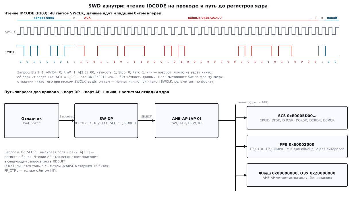
The figure was recorded from the model: on every SWCLK edge you can see who drives the line.
One read is 48 cycles: 8 request, 1 turnaround, 3 response, 33 data with parity,
1 turnaround and 2 idle cycles that swd_xfer adds after each exchange.
A write also took 48 cycles. At 2 MHz, where OpenOCD starts
(35б.2), that is 24 µs per exchange. Over the whole run the debugger and the target never
drove the line at the same time: 0 collisions in 17233 cycles.
The pins for a real STM32 are PB13 (SWCLK) and PB14 (SWDIO), through registers:
/* pins_stm32.c — ножки отладчика на STM32: SWCLK — PB13, SWDIO — PB14 (раздел 35д).
 * Собирается для F103 (-DSTM32F10X_MD) и F407 (-DSTM32F407xx). На плате не проверялось. */
#if defined(STM32F10X_MD)
#include "stm32f10x.h"
#else
#include "stm32f4xx.h"
#endif
#include "swd_host.h"

void pins_init(void)
{
    GPIOB->BSRR = (1u << 13) | (1u << 14);                       /* обе линии в единицу */
#if defined(STM32F10X_MD)
    RCC->APB2ENR |= RCC_APB2ENR_IOPBEN;
    GPIOB->CRH = (GPIOB->CRH & ~0x0FF00000u) | 0x03300000u;      /* PB13, PB14: выход 50 МГц */
#else
    RCC->AHB1ENR |= RCC_AHB1ENR_GPIOBEN;
    GPIOB->PUPDR = (GPIOB->PUPDR & ~(3u << 28)) | (1u << 28);    /* PB14: подтяжка вверх */
    GPIOB->OSPEEDR |= (3u << 26) | (3u << 28);
    GPIOB->MODER = (GPIOB->MODER & ~(0xFu << 26)) | (5u << 26);  /* PB13, PB14: выход */
#endif
}

void pin_swclk(int level)   { GPIOB->BSRR = level ? 1u << 13 : 1u << (13 + 16); }
void pin_swdio_out(int bit) { GPIOB->BSRR = bit ? 1u << 14 : 1u << (14 + 16); }
int  pin_swdio_in(void)     { return (int)(GPIOB->IDR >> 14 & 1u); }

void pin_swdio_dir(int out)
{
#if defined(STM32F10X_MD)
    if (!out) GPIOB->BSRR = 1u << 14;                            /* у F1 вход с подтяжкой вверх — по ODR = 1 */
    GPIOB->CRH = (GPIOB->CRH & ~0x0F000000u) | (out ? 0x03000000u : 0x08000000u);
#else
    GPIOB->MODER = (GPIOB->MODER & ~(3u << 28)) | ((uint32_t)out << 28);
#endif
}
On F1, the input with pull-up is enabled only with a one in ODR (RM0008,
table 20: "Input pull-up" — ODR = 1, "Input pull-down" — ODR = 0),
so a one is written to ODR before switching to input. Without delays
the pins toggle as fast as the core allows; the SWCLK frequency on a board
was not measured. The debugger code swd_host.c took 1248 bytes for Cortex-M3 and for
Cortex-M4 alike, the pins — 148 bytes for F103 and 144 bytes for F407
(arm-none-eabi-gcc 12.2.1, -Os).
35д.2 Connecting: the JTAG→SWD switch, line reset, IDCODE, power
After power-up the STM32 runs the JTAG-DP port. To switch to SWD, RM0008 and RM0090 (31.3.1 and 38.3.1) say to send more than 50 ones on SWDIO, the 16 bits 0111100111100111 (most significant bit first) and again more than 50 ones. Least significant bit first, this number is 0xE79E. More than 50 ones in a row is also a line reset. After a reset you need at least two zero cycles (idle), and the first thing to do is read IDCODE. Otherwise, per the RM, the port answers FAULT to any other request.
void swd_bits(int n, uint32_t bits)       /* до 32 бит, младший первым */
{
    pin_swdio_dir(1);
    for (int i = 0; i < n; i++) bit_out((int)(bits >> i & 1u));
}

void swd_line_reset(void)                 /* 56 единиц и 8 тактов покоя */
{
    swd_bits(28, 0x0FFFFFFFu);
    swd_bits(28, 0x0FFFFFFFu);
    swd_bits(8, 0);
    sel_cache = 0xFFFFFFFFu;
}

void swd_jtag_to_swd(void)                /* RM0008/RM0090: >50 единиц, 0xE79E, >50 единиц */
{
    swd_bits(28, 0x0FFFFFFFu);
    swd_bits(28, 0x0FFFFFFFu);
    swd_bits(16, 0xE79Eu);
    swd_line_reset();
}
int swd_connect(uint32_t *idcode)
{
    uint32_t cs = 0;
    swd_jtag_to_swd();
    int ack = dp_read(DP_IDCODE, idcode);  /* после сброса линии — первым делом */
    if (ack != ACK_OK) return ack;
    dp_write(DP_ABORT, 0x1Eu);            /* стереть залипшие флаги ошибок */
    dp_write(DP_CTRL_STAT, 0x50000000u);  /* CSYSPWRUPREQ | CDBGPWRUPREQ */
    for (int i = 0; i < 10; i++) {
        ack = dp_read(DP_CTRL_STAT, &cs);
        if (ack == ACK_OK && (cs & 0xA0000000u) == 0xA0000000u) return ACK_OK;
    }
    return ACK_FAULT;
}
pyocd connects with the same sequence: in its probe/swj.py the switch
to SWD is swj_sequence(16, 0xe79e). The model recognized it from pyocd too.
Run on the model:
| What was done | Response |
|---|---|
| Line reset without the JTAG→SWD switch, IDCODE read | silence: 0b111 |
| JTAG→SWD switch, immediate CTRL/STAT read | FAULT |
| Line reset, IDCODE read | OK |
| CTRL/STAT = 0x50000000, CTRL/STAT read | 0xF0000000 |
"Silence" means the target does not drive the line, and the pull-up gives three ones. This is not an ACK, but its absence; the debugger must tell it apart from FAULT.
The SW-DP IDCODE per the RM is 0x1BA01477 on F103 (Cortex-M3 r1p1) and 0x2BA01477
on F407 (Cortex-M4 r0p1); the model answers with these numbers. Through JTAG the same
cores have a different code — 0x3BA00477 and 0x4BA00477; do not mix them up. The code of the
chip itself lies in DBGMCU_IDCODE at address 0xE0042000; the RM advises
identifying the microcontroller by it. The device number in the low 12 bits is
0x410 for medium-density F103 and 0x413 for F405/F407.
Writing CTRL/STAT with the bits CSYSPWRUPREQ (30) and CDBGPWRUPREQ (28) requests power for debugging; the target acknowledges with bits 31 and 29, and CTRL/STAT reads as 0xF0000000. Until the acknowledgement arrives, the AP port is not accessed.
35д.3 The AP port: memory through CSW, TAR and DRW
The DP port is just four registers: IDCODE (a write to the same address is ABORT), CTRL/STAT, SELECT and RDBUFF. Everything else is done by the access port. STM32F1 and F4 have one — the AHB-AP (RM0008, 31.9; RM0090, 38.9): a master on the bus that sees all memory except the ICode bus. Its registers:
| Address | Register | What it does |
|---|---|---|
| 0x00 | CSW | access size, address auto-increment, attributes |
| 0x04 | TAR | memory address |
| 0x0C | DRW | data: read or write at the address from TAR |
| 0x10…0x1C | BD0…BD3 | four words next to TAR without rewriting it |
| 0xF8 | BASE | ROM table address |
| 0xFC | IDR | what kind of port this is |
An AP register address is eight bits. The upper four come from SELECT (the APBANKSEL field, bits 7:4), the lower ones from A[2:3] of the request; the port number is in bits 31:24 of SELECT. To read IDR, 0xF0 is written to SELECT, and the request goes with A = 0xC.
The second peculiarity: AP reads are posted. The response to an AP read request is the result of the previous AP read. The fresh result arrives in the next AP request or in the DP's RDBUFF (RM0008, 31.8.4). So a single read is a request to the AP followed by a read of RDBUFF:
static int ap_select(uint32_t reg)        /* APSEL = 0, банк — reg[7:4] */
{
    uint32_t sel = reg & 0xF0u;
    if (sel == sel_cache) return ACK_OK;
    int ack = dp_write(DP_SELECT, sel);
    if (ack == ACK_OK) sel_cache = sel;
    return ack;
}

int ap_read(uint32_t reg, uint32_t *v)    /* чтение AP отложено: результат — в RDBUFF */
{
    uint32_t stale;
    int ack = ap_select(reg);
    if (ack == ACK_OK) ack = xfer_retry(1, 1, (int)(reg & 0xCu), &stale);
    if (ack == ACK_OK) ack = dp_read(DP_RDBUFF, v);
    return ack;
}

int ap_write(uint32_t reg, uint32_t v)
{
    int ack = ap_select(reg);
    return ack == ACK_OK ? xfer_retry(1, 0, (int)(reg & 0xCu), &v) : ack;
}
int mem_read32(uint32_t addr, uint32_t *v)
{
    int ack = ap_write(AP_CSW, 0x23000002u);   /* слово, без автоинкремента */
    if (ack == ACK_OK) ack = ap_write(AP_TAR, addr);
    if (ack == ACK_OK) ack = ap_read(AP_DRW, v);
    return ack;
}

int mem_write32(uint32_t addr, uint32_t v)
{
    int ack = ap_write(AP_CSW, 0x23000002u);
    if (ack == ACK_OK) ack = ap_write(AP_TAR, addr);
    if (ack == ACK_OK) ack = ap_write(AP_DRW, v);
    return ack;
}

int mem_read_block(uint32_t addr, int n, uint32_t *buf)   /* TAR сам растёт на 4 */
{
    uint32_t prev;
    int ack = ap_write(AP_CSW, 0x23000012u);
    if (ack == ACK_OK) ack = ap_write(AP_TAR, addr);
    if (ack == ACK_OK) ack = ap_select(AP_DRW);
    if (ack == ACK_OK) ack = xfer_retry(1, 1, AP_DRW, &prev);      /* ответ — прошлое чтение */
    for (int i = 1; i < n && ack == ACK_OK; i++)
        ack = xfer_retry(1, 1, AP_DRW, &buf[i - 1]);                 /* каждый ответ — предыдущее слово */
    if (ack == ACK_OK) ack = dp_read(DP_RDBUFF, &buf[n - 1]);       /* последнее — из RDBUFF */
    return ack;
}
ap_select remembers what is already in SELECT and does not write it again needlessly.
A memory word cost 4 requests in the run (CSW, TAR, DRW, RDBUFF), and the first one
after a bank change — 5. At 2 MHz, four requests of 48 cycles are 96 µs.
A block of four words with auto-increment took 7 requests instead of 16: CSW, TAR,
four DRW reads, each returning the previous word, and RDBUFF
with the last one. Read back: 20005000, 08000009, 20004902, 60083001 — the initial
stack pointer, the reset vector and the first instructions of the program.
What the debugger read from the model through the AP (F407 in the second column):
| Address or register | F103 | F407 |
|---|---|---|
| AP IDR | 0x24770011 | 0x24770011 |
| AP BASE | 0xE00FF003 | 0xE00FF003 |
| CPUID, 0xE000ED00 | 0x411FC231 | 0x410FC241 |
| DBGMCU_IDCODE, 0xE0042000 | 0x20036410 | 0x10076413 |
| first ROM table entry, 0xE00FF000 | 0xFFF0F003 → SCS at 0xE000E000 | same |
These are the model's values: that is how it was configured, and that is how pyocd decoded them. Its
log shows "AHB-AP#0 IDR = 0x24770011", four components from the ROM table
(SCS, DWT, FPB, ITM) and "CPU core #0: Cortex-M3 r1p1" for F103,
"Cortex-M4 r0p1" for F407. These numbers were not checked against a real chip,
except IDCODE and the code in DBGMCU_IDCODE, which are taken from the RM.
The AP port works while the core is running. The model's program adds one to r0
in a loop and writes it to address 0x20000000. Two reads of this address through
the AP, 100 SWCLK cycles apart, gave 612 and 710: the core was not
halted. RTT from 21а is built on exactly this.
35д.4 WAIT, FAULT and silence
WAIT means "bus busy, try again". The debugger repeats the same request:
static int xfer_retry(int apndp, int rnw, int a, uint32_t *data)
{
    for (int tries = 0; tries < 100; tries++) {
        int ack = swd_xfer(apndp, rnw, a, data);
        if (ack != ACK_WAIT) return ack;
        swd_waits++;                      /* шина занята: тот же запрос ещё раз */
    }
    return ACK_WAIT;
}

int dp_read(int a, uint32_t *v)  { return xfer_retry(0, 1, a, v); }
int dp_write(int a, uint32_t v)  { return xfer_retry(0, 0, a, &v); }
In the model, after a flash read the bus stays busy for three more requests. A read
of the word at 0x08000004 went through with three WAIT responses: 7 requests instead of 4,
the result is correct — 0x08000009. SW_DP.c from CMSIS-DAP on the same model also
got three WAITs and the same word. CMSIS-DAP repeats the request as many times
as it is told (retry_count in DAP_Data); in our own debugger this is
xfer_retry above.
FAULT is an error that sticks. A read at address 0x60000000, where the model has nothing, itself completed with OK: the read is posted. The bus error set STICKYERR (bit 5 of CTRL/STAT), and the next request got the FAULT — the read of RDBUFF. From then on all AP requests get FAULT, even to valid memory:
| Step | Result |
|---|---|
| Read 0x60000000 | FAULT, CTRL/STAT = 0xF0000020 |
| Read 0x20000000 | FAULT |
| ABORT = 0x04 (STKERRCLR) | CTRL/STAT = 0xF0000000 |
| Read 0x20000000 | OK |
pyocd got TransferFaultError on the same steps and cleared the flag itself: its
next read of 0x20000000 went through.
Silence is the response 0b111. It happens when the target did not understand the request. In the run the debugger sent the header 0x85 — that is 0xA5 with the parity bit flipped. The model went silent and stayed silent on the next correct IDCODE request as well; after a line reset IDCODE was read. This is the model's behavior; for a real port RM0008 and RM0090 do not describe such cases.
35д.5 Halting the core: DHCSR, DCRSR, DCRDR, DEMCR
Through the AP the debugger writes to ordinary memory addresses. It controls the core
with four registers in the SCS area (CoreDebug_BASE = 0xE000EDF0
in core_cm3.h and core_cm4.h):
| Address | Register | Main bits |
|---|---|---|
| 0xE000EDF0 | DHCSR | 0 C_DEBUGEN, 1 C_HALT, 2 C_STEP; 16 S_REGRDY, 17 S_HALT, 24 S_RETIRE_ST, 25 S_RESET_ST; writes only with DBGKEY in bits 31:16 |
| 0xE000EDF4 | DCRSR | 4:0 REGSEL — core register number, 16 REGWnR — write |
| 0xE000EDF8 | DCRDR | core register value |
| 0xE000EDFC | DEMCR | 0 VC_CORERESET — halt on reset, 24 TRCENA — enable DWT and ITM |
The DBGKEY key is 0xA05F (as in pyocd and in OpenOCD scripts). A write to DHCSR
without it does not take effect. In the run,
writing 0x00000003 (C_HALT and C_DEBUGEN without the key) did not halt the core:
DHCSR stayed 0x01010000, the core is running. Writing 0xA05F0003 halted it:
DHCSR = 0x00030003 (S_HALT, S_REGRDY, C_HALT, C_DEBUGEN), and DFSR has the
HALTED bit. OpenOCD does the same write in its script for MAX32xxx
(target/max32xxx_common.cfg, OpenOCD 0.12.0, GPL-2.0):
mww 0xE000EDF0 [expr {$DBGKEY | $C_HALT | $C_DEBUGEN}] with DBGKEY = 0xA05F0000.
A core register is read in three steps: the number into DCRSR, wait for S_REGRDY, the value from DCRDR. Numbers: 0…12 — R0…R12, 13 — SP, 14 — LR, 15 — the return address from the halt (that is, PC), 16 — xPSR, 17 — MSP, 18 — PSP.
static int wait_dhcsr(uint32_t mask)
{
    uint32_t v = 0;
    for (int i = 0; i < 100; i++)
        if (mem_read32(DHCSR, &v) == ACK_OK && (v & mask)) return ACK_OK;
    return ACK_FAULT;
}

int core_halt(void)
{
    int ack = mem_write32(DHCSR, DBGKEY | 0x3u);   /* C_HALT | C_DEBUGEN */
    return ack == ACK_OK ? wait_dhcsr(1u << 17) : ack;   /* S_HALT */
}

int core_run(void)  { return mem_write32(DHCSR, DBGKEY | 0x1u); }

int core_step(void)
{
    int ack = mem_write32(DHCSR, DBGKEY | 0x5u);   /* C_STEP | C_DEBUGEN, C_HALT = 0 */
    return ack == ACK_OK ? wait_dhcsr(1u << 17) : ack;
}

int core_reg_read(int n, uint32_t *v)              /* n: 0…12 R0…R12, 13 SP, 14 LR, 15 PC, 16 xPSR */
{
    int ack = mem_write32(DCRSR, (uint32_t)n);     /* REGWnR = 0: чтение */
    if (ack == ACK_OK) ack = wait_dhcsr(1u << 16); /* S_REGRDY */
    if (ack == ACK_OK) ack = mem_read32(DCRDR, v);
    return ack;
}
After the halt the debugger read R0 = 962, R1 = 0x20000000, SP = 0x20005000, PC = 0x0800000C, xPSR = 0x01000000, and in memory at 0x20000000 — also 962. Over the next 200 SWCLK cycles the halted core did not execute a single instruction.
Halt on reset. RM0008 (31.10) describes it like this: VC_CORERESET
in DEMCR and C_DEBUGEN in DHCSR. A system reset does not touch the debug registers.
The debugger wrote DEMCR = 0x01000001 and reset the core by writing 0x05FA0004
to AIRCR (SYSRESETREQ with the key 0x05FA). The model's core stopped at the first instruction:
PC = 0x08000008, SP = 0x20005000 from vector 0, DFSR = 0x00000008 (VCATCH),
DHCSR = 0x02030003 — with the S_RESET_ST flag. The pyocd command reset_and_halt
gave the same PC on the model.
35д.6 FPB breakpoints
The six hardware breakpoints from 35.1 are the FPB unit at address 0xE0002000. RM0008 (31.12) and RM0090 (38.12) state: 6 instruction comparators and 2 literal comparators. Instruction comparators either replace an instruction or give the core a halt instruction; one or the other.
| Register | Fields |
|---|---|
| FP_CTRL, 0xE0002000 | 0 ENABLE, 1 KEY — without it the write does not take effect, 7:4 NUM_CODE1, 11:8 NUM_LIT, 13:12 NUM_CODE2 |
| FP_COMP0…7, 0xE0002008…0xE0002024 | 0 ENABLE, 28:2 COMP — word address, 31:30 REPLACE: 01 — lower halfword, 10 — upper, 11 — both |
The model answers FP_CTRL = 0x00000260: 6 instruction comparators, 2 literal ones,
0 in bits 31:28 (REV); per pyocd this is a first-version FPB. This gives the main
limitation. Only bits 28:2 fit into COMP, so a breakpoint can only be set
in the code region 0x00000000…0x1FFFFFFF. STM32 flash memory at 0x08000000
falls into it, RAM at 0x20000000 does not. For code in RAM the debugger writes
a BKPT instruction into memory: this is a software breakpoint, and it needs no FPB.
fpb_set refuses address 0x20000100 right away.
int fpb_set(int n, uint32_t addr)                  /* FPB v1: только 0x00000000…0x1FFFFFFF */
{
    if (addr >= 0x20000000u) return ACK_FAULT;
    uint32_t rep = (addr & 2u) ? 2u : 1u;          /* 10 — старшее полуслово, 01 — младшее */
    int ack = mem_write32(FP_CTRL, 0x3u);          /* KEY | ENABLE */
    if (ack == ACK_OK) ack = mem_write32(FP_COMP(n), rep << 30 | (addr & 0x1FFFFFFCu) | 1u);
    return ack;
}

int fpb_clear(int n) { return mem_write32(FP_COMP(n), 0); }
The model core's program is five instructions. It was assembled with arm-none-eabi-as, and the bytes
matched those stored in the model:
@ prog35f.s — программа, которую исполняет ядро модели (раздел 35д).
        .syntax unified
        .cpu    cortex-m3
        .thumb
        .section .text
        .p2align 2
        .word   0x20005000          @ 0x08000000: начальный SP
        .word   reset + 1           @ 0x08000004: вектор сброса (Thumb)
reset:  ldr     r1, ram          @ 0x08000008: литерал из флеш-памяти
        movs    r0, #0              @ 0x0800000A
loop:   adds    r0, #1              @ 0x0800000C
        str     r0, [r1]            @ 0x0800000E
        b       loop                @ 0x08000010
        nop                         @ 0x08000012
ram:    .word   0x20000000          @ 0x08000014
The model checks for a matching comparator like this — before executing the instruction:
static int fpb_hit(uint32_t pc)                          /* FPB v1: только код 0…0x1FFFFFFF */
{
    if (!(fp_ctrl & 1u)) return 0;
    for (int i = 0; i < 6; i++) {
        uint32_t c = fp_comp[i];
        if (!(c & 1u) || (c & 0x1FFFFFFCu) != (pc & 0x1FFFFFFCu)) continue;
        uint32_t rep = c >> 30;
        if (rep == 3 || (rep == 1 && !(pc & 2u)) || (rep == 2 && (pc & 2u))) return 1;
    }
    return 0;
}
Experiment: a breakpoint on str r0, [r1] at address 0x0800000E. The address lies in the upper
halfword of the word 0x0800000C, so REPLACE = 10, and FP_COMP0 got
0x8800000D. pyocd wrote the same 0x8800000D for the same breakpoint.
| Step | PC | R0 | Memory 0x20000000 | DFSR |
|---|---|---|---|---|
| Breakpoint set, core started | 0x0800000E | 963 | 962 | 0x00000002, BKPT |
| Started again without removing the breakpoint | 0x0800000E | 963 | 962 | instructions executed: 0 |
| Removed, step, restored, started | 0x0800000E | 964 | 963 | instructions executed: 3 |
The core stops before the instruction at the breakpoint: R0 is already 963, but memory has not been written yet.
If you simply continue, the core hits the same instruction again and stops without
making a single step. So before continuing the debugger removes the breakpoint, makes
a step (C_STEP), puts the breakpoint back and only then lets the core run. After the step
PC = 0x08000010, DFSR has HALTED. pyocd does the same on the model: after
remove_breakpoint and step PC became 0x08000010.
A read of flash memory through the AP does not see the breakpoint: at address 0x0800000C the debugger
read 0x60083001 — the real adds and str instructions. RM0008 says exactly
this: AHB-AP accesses bypass the FPB.
The four watchpoints from 35.1 are DWT comparators; in the model the NUMCOMP field of the DWT_CTRL register (0xE0001000) equals 4, as RM0008 and RM0090 state. The DWT itself is covered in 75а.6.
35д.7 Pitfalls
The ACK is read backwards. In the RM0008 table OK is written as "100". That is the order on the wire, while as a number OK = 0b001. A debugger that compares with 0b100 takes OK for FAULT. In JTAG the codes are different: there "010" is OK or FAULT, "001" is WAIT.
Request parity including the start bit. The start bit is always 1. If you include it in the parity, the parity bit will always be wrong. The target stays silent (0b111), and it seems that it is not connected.
After a line reset — IDCODE first. Any other request gets FAULT (RM0008, 31.8.3). A debugger that writes ABORT or CTRL/STAT right away sees FAULT on a working board.
Silence is confused with FAULT. Three ones are the pull-up, not a response. Silence happens when the target is not in SWD (there was no JTAG→SWD switch), when there is no power or wire, when the debugger got the header wrong. It is cured by a line reset and an IDCODE read, not by ABORT.
The first AP read returns garbage. The response to an AP read is the result of the previous read. Whoever takes the data straight from the response gets the previous word. A single read ends with a read of RDBUFF.
An error "out of nowhere". FAULT arrives not on the request that caused it, but on the next AP request. Until ABORT is written with STKERRCLR, every request gets FAULT, even to valid memory.
DHCSR without the key. A write without 0xA05F in the upper bits silently disappears: no error, no halt. FP_CTRL likewise requires the KEY bit.
A breakpoint in RAM. A first-version FPB sees only addresses up to 0x1FFFFFFF. Code moved to RAM is halted with a BKPT instruction in memory — and it must be removed before the debugger disconnects: without a debugger, BKPT leads to a HardFault (35а.3).
Continue from a breakpoint — stop on it again. The core halts before the instruction. First remove the breakpoint, step, restore the breakpoint, then let it run.
pyocd 0.45.1 counts literals wrong. Its log on the model says "6 hardware
breakpoints, 4 literal comparators" with FP_CTRL = 0x00000260, where NUM_LIT
(bits 11:8) equals 2. In pyocd/coresight/fpb.py the field is taken with a shift by 7,
not by 8. This does not affect breakpoints: pyocd does not use literals.
35д.8 Summary
- An SWD exchange is 8 request bits, a turnaround, 3 response bits, 32 data bits with parity. With two idle cycles — 48 cycles, at 2 MHz 24 µs.
- Headers: IDCODE read 0xA5, CTRL/STAT write 0xA9, DRW read 0x9F, RDBUFF read 0xBD. Parity is over four bits without the start bit; ACK OK on the wire starts with a one.
- Connecting: more than 50 ones, 0xE79E, more than 50 ones, idle, IDCODE (0x1BA01477 on F103, 0x2BA01477 on F407), power through CTRL/STAT 0x50000000 → 0xF0000000.
- Memory goes through the AHB-AP: CSW, TAR, DRW. AP reads are posted. A word takes 4 requests, a block of 4 words with auto-increment — 7. You can read on the fly: 612 → 710.
- WAIT — repeat; FAULT sticks until ABORT; silence 0b111 is cured by a line reset.
- Core: DHCSR with the key 0xA05F halts it (0x00030003), DCRSR and DCRDR read registers, DEMCR.VC_CORERESET and AIRCR give a halt on reset (PC = 0x08000008).
- FPB v1: 6 instruction comparators and 2 literal ones, only addresses up to 0x1FFFFFFF; a breakpoint at 0x0800000E gives FP_COMP0 = 0x8800000D, and pyocd wrote the same.
- Our own debugger is 1248 bytes on Cortex-M3 and M4. The model was checked by SW_DP.c from CMSIS-DAP and pyocd 0.45.1; nothing was run on a board.
Full source code
swd_host.c — an SWD debugger on two pins: packets, the DP and AP ports, memory, halt, FPB.
/* swd_host.c — отладчик SWD на двух ножках (раздел 35д): пакеты, чётность,
 * WAIT, порты DP и AP, память, DHCSR/DCRSR и точки останова FPB. */
#include "swd_host.h"

uint32_t swd_waits;
static uint32_t sel_cache = 0xFFFFFFFFu;  /* что сейчас в DP SELECT */

static void bit_out(int b)                /* отладчик меняет линию при низком SWCLK */
{
    pin_swdio_out(b);
    pin_swclk(0);
    pin_swclk(1);                         /* цель читает по фронту вверх */
}

static int bit_in(void)                   /* цель выставила бит по прошлому фронту */
{
    pin_swclk(0);
    int b = pin_swdio_in();
    pin_swclk(1);
    return b;
}

static void turnaround(void)              /* такт, когда линию не ведёт никто */
{
    pin_swclk(0);
    pin_swclk(1);
}

static int parity32(uint32_t v)
{
    v ^= v >> 16; v ^= v >> 8; v ^= v >> 4; v ^= v >> 2; v ^= v >> 1;
    return (int)(v & 1u);
}

uint8_t swd_header(int apndp, int rnw, int a)
{
    uint32_t a23 = (uint32_t)(a >> 2) & 3u;
    uint32_t body = (uint32_t)apndp | (uint32_t)rnw << 1 | a23 << 2;      /* APnDP, RnW, A[2:3] */
    return (uint8_t)(1u | body << 1 | (uint32_t)parity32(body) << 5 | 0u << 6 | 1u << 7);
}                                         /* Start=1 … Parity, Stop=0, Park=1 */

void swd_bits(int n, uint32_t bits)       /* до 32 бит, младший первым */
{
    pin_swdio_dir(1);
    for (int i = 0; i < n; i++) bit_out((int)(bits >> i & 1u));
}

void swd_line_reset(void)                 /* 56 единиц и 8 тактов покоя */
{
    swd_bits(28, 0x0FFFFFFFu);
    swd_bits(28, 0x0FFFFFFFu);
    swd_bits(8, 0);
    sel_cache = 0xFFFFFFFFu;
}

void swd_jtag_to_swd(void)                /* RM0008/RM0090: >50 единиц, 0xE79E, >50 единиц */
{
    swd_bits(28, 0x0FFFFFFFu);
    swd_bits(28, 0x0FFFFFFFu);
    swd_bits(16, 0xE79Eu);
    swd_line_reset();
}

int swd_xfer(int apndp, int rnw, int a, uint32_t *data)
{
    uint8_t h = swd_header(apndp, rnw, a);
    pin_swdio_dir(1);
    for (int i = 0; i < 8; i++) bit_out(h >> i & 1);
    pin_swdio_dir(0);
    turnaround();
    int ack = bit_in() | bit_in() << 1 | bit_in() << 2;
    if (ack != ACK_OK) {                  /* WAIT, FAULT или тишина (линия подтянута: 0b111) */
        turnaround();
        pin_swdio_dir(1);
        swd_bits(2, 0);
        return ack;
    }
    if (rnw) {
        uint32_t v = 0;
        for (int i = 0; i < 32; i++) v |= (uint32_t)bit_in() << i;
        int p = bit_in();
        turnaround();
        pin_swdio_dir(1);
        swd_bits(2, 0);
        if (p != parity32(v)) return ACK_PARITY;
        *data = v;
    } else {
        turnaround();
        pin_swdio_dir(1);
        for (int i = 0; i < 32; i++) bit_out((int)(*data >> i & 1u));
        bit_out(parity32(*data));
        swd_bits(2, 0);                   /* два такта покоя: запись доходит до шины */
    }
    return ACK_OK;
}

static int xfer_retry(int apndp, int rnw, int a, uint32_t *data)
{
    for (int tries = 0; tries < 100; tries++) {
        int ack = swd_xfer(apndp, rnw, a, data);
        if (ack != ACK_WAIT) return ack;
        swd_waits++;                      /* шина занята: тот же запрос ещё раз */
    }
    return ACK_WAIT;
}

int dp_read(int a, uint32_t *v)  { return xfer_retry(0, 1, a, v); }
int dp_write(int a, uint32_t v)  { return xfer_retry(0, 0, a, &v); }

static int ap_select(uint32_t reg)        /* APSEL = 0, банк — reg[7:4] */
{
    uint32_t sel = reg & 0xF0u;
    if (sel == sel_cache) return ACK_OK;
    int ack = dp_write(DP_SELECT, sel);
    if (ack == ACK_OK) sel_cache = sel;
    return ack;
}

int ap_read(uint32_t reg, uint32_t *v)    /* чтение AP отложено: результат — в RDBUFF */
{
    uint32_t stale;
    int ack = ap_select(reg);
    if (ack == ACK_OK) ack = xfer_retry(1, 1, (int)(reg & 0xCu), &stale);
    if (ack == ACK_OK) ack = dp_read(DP_RDBUFF, v);
    return ack;
}

int ap_write(uint32_t reg, uint32_t v)
{
    int ack = ap_select(reg);
    return ack == ACK_OK ? xfer_retry(1, 0, (int)(reg & 0xCu), &v) : ack;
}

int swd_connect(uint32_t *idcode)
{
    uint32_t cs = 0;
    swd_jtag_to_swd();
    int ack = dp_read(DP_IDCODE, idcode);  /* после сброса линии — первым делом */
    if (ack != ACK_OK) return ack;
    dp_write(DP_ABORT, 0x1Eu);            /* стереть залипшие флаги ошибок */
    dp_write(DP_CTRL_STAT, 0x50000000u);  /* CSYSPWRUPREQ | CDBGPWRUPREQ */
    for (int i = 0; i < 10; i++) {
        ack = dp_read(DP_CTRL_STAT, &cs);
        if (ack == ACK_OK && (cs & 0xA0000000u) == 0xA0000000u) return ACK_OK;
    }
    return ACK_FAULT;
}

int mem_read32(uint32_t addr, uint32_t *v)
{
    int ack = ap_write(AP_CSW, 0x23000002u);   /* слово, без автоинкремента */
    if (ack == ACK_OK) ack = ap_write(AP_TAR, addr);
    if (ack == ACK_OK) ack = ap_read(AP_DRW, v);
    return ack;
}

int mem_write32(uint32_t addr, uint32_t v)
{
    int ack = ap_write(AP_CSW, 0x23000002u);
    if (ack == ACK_OK) ack = ap_write(AP_TAR, addr);
    if (ack == ACK_OK) ack = ap_write(AP_DRW, v);
    return ack;
}

int mem_read_block(uint32_t addr, int n, uint32_t *buf)   /* TAR сам растёт на 4 */
{
    uint32_t prev;
    int ack = ap_write(AP_CSW, 0x23000012u);
    if (ack == ACK_OK) ack = ap_write(AP_TAR, addr);
    if (ack == ACK_OK) ack = ap_select(AP_DRW);
    if (ack == ACK_OK) ack = xfer_retry(1, 1, AP_DRW, &prev);      /* ответ — прошлое чтение */
    for (int i = 1; i < n && ack == ACK_OK; i++)
        ack = xfer_retry(1, 1, AP_DRW, &buf[i - 1]);                 /* каждый ответ — предыдущее слово */
    if (ack == ACK_OK) ack = dp_read(DP_RDBUFF, &buf[n - 1]);       /* последнее — из RDBUFF */
    return ack;
}

static int wait_dhcsr(uint32_t mask)
{
    uint32_t v = 0;
    for (int i = 0; i < 100; i++)
        if (mem_read32(DHCSR, &v) == ACK_OK && (v & mask)) return ACK_OK;
    return ACK_FAULT;
}

int core_halt(void)
{
    int ack = mem_write32(DHCSR, DBGKEY | 0x3u);   /* C_HALT | C_DEBUGEN */
    return ack == ACK_OK ? wait_dhcsr(1u << 17) : ack;   /* S_HALT */
}

int core_run(void)  { return mem_write32(DHCSR, DBGKEY | 0x1u); }

int core_step(void)
{
    int ack = mem_write32(DHCSR, DBGKEY | 0x5u);   /* C_STEP | C_DEBUGEN, C_HALT = 0 */
    return ack == ACK_OK ? wait_dhcsr(1u << 17) : ack;
}

int core_reg_read(int n, uint32_t *v)              /* n: 0…12 R0…R12, 13 SP, 14 LR, 15 PC, 16 xPSR */
{
    int ack = mem_write32(DCRSR, (uint32_t)n);     /* REGWnR = 0: чтение */
    if (ack == ACK_OK) ack = wait_dhcsr(1u << 16); /* S_REGRDY */
    if (ack == ACK_OK) ack = mem_read32(DCRDR, v);
    return ack;
}

int fpb_set(int n, uint32_t addr)                  /* FPB v1: только 0x00000000…0x1FFFFFFF */
{
    if (addr >= 0x20000000u) return ACK_FAULT;
    uint32_t rep = (addr & 2u) ? 2u : 1u;          /* 10 — старшее полуслово, 01 — младшее */
    int ack = mem_write32(FP_CTRL, 0x3u);          /* KEY | ENABLE */
    if (ack == ACK_OK) ack = mem_write32(FP_COMP(n), rep << 30 | (addr & 0x1FFFFFFCu) | 1u);
    return ack;
}

int fpb_clear(int n) { return mem_write32(FP_COMP(n), 0); }
Next: section 36 "Typical problems" — a summary table "symptom → cause → fix" for the whole handbook.