 Embedded HandbookApps
Appendix A17. STM32WB register maps
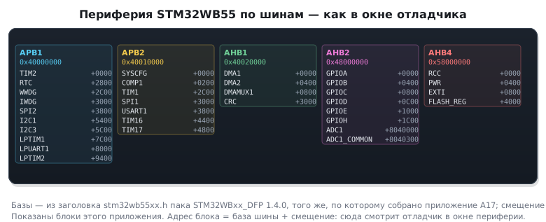
The STM32WB series: Cortex-M4 with Bluetooth LE and Zigbee radio on a second core. Registers and bits of the main blocks come from the STM32WB55 header, made by the same generator as the F1 and F4 maps: offsets from the *_TypeDef structures, register purposes and bit descriptions from the header comments. Blocks the series lacks are left out. For low power, see PWR (sleep modes), RCC (the LSE/LSI/MSI oscillators), LPTIM and LPUART — they keep working in sleep. The handbook sections are written for the F103 and F407; register and bit names are mostly the same across series — the map helps move code over and see what is arranged differently.
How to read: the offset is from the block's base address; 31:16 is a bit field
from 16 to 31; a single number is a single bit. The number in brackets in a block
heading is the section where the block is covered.
RCC — Clocks (section 6)
| Register | Offset | Bits | Purpose |
|---|---|---|---|
CR |
0x00 |
32 | RCC clock Control Register |
RCC_CR_MSION |
0 | Internal Multi Speed oscillator (MSI) clock enable | |
RCC_CR_MSIRDY |
1 | Internal Multi Speed oscillator (MSI) clock ready flag | |
RCC_CR_MSIPLLEN |
2 | Internal Multi Speed oscillator (MSI) PLL enable | |
RCC_CR_MSIRANGE |
4:7 | Internal Multi Speed oscillator (MSI) clock Range | |
RCC_CR_HSION |
8 | Internal High Speed oscillator (HSI16) clock enable | |
RCC_CR_HSIKERON |
9 | Internal High Speed oscillator (HSI16) clock enable for some IPs Kernel | |
RCC_CR_HSIRDY |
10 | Internal High Speed oscillator (HSI16) clock ready flag | |
RCC_CR_HSIASFS |
11 | HSI16 Automatic Start from Stop | |
RCC_CR_HSIKERDY |
12 | Internal High Speed oscillator (HSI16) clock enable for some IPs Kernel ready flag | |
RCC_CR_HSEON |
16 | External High Speed oscillator (HSE) clock enable | |
RCC_CR_HSERDY |
17 | External High Speed oscillator (HSE) clock ready | |
RCC_CR_CSSON |
19 | HSE Clock Security System enable | |
RCC_CR_HSEPRE |
20 | HSE sysclk prescaler | |
RCC_CR_PLLON |
24 | System PLL clock enable | |
RCC_CR_PLLRDY |
25 | System PLL clock ready | |
RCC_CR_PLLSAI1ON |
26 | SAI1 PLL enable | |
RCC_CR_PLLSAI1RDY |
27 | SAI1 PLL ready | |
ICSCR |
0x04 |
32 | RCC Internal Clock Sources Calibration Register |
RCC_ICSCR_MSICAL |
0:7 | MSICAL[7:0] bits | |
RCC_ICSCR_MSITRIM |
8:15 | MSITRIM[7:0] bits | |
RCC_ICSCR_HSICAL |
16:23 | HSICAL[7:0] bits | |
RCC_ICSCR_HSITRIM |
24:30 | HSITRIM[6:0] bits | |
CFGR |
0x08 |
32 | RCC Clocks Configuration Register |
RCC_CFGR_SW |
0:1 | SW[1:0] bits (System clock Switch) | |
RCC_CFGR_SWS |
2:3 | SWS[1:0] bits (System Clock Switch Status) | |
RCC_CFGR_HPRE |
4:7 | HPRE[3:0] bits (AHB prescaler) | |
RCC_CFGR_PPRE1 |
8:10 | PRE1[2:0] bits (APB1 prescaler) | |
RCC_CFGR_PPRE2 |
11:13 | PRE2[2:0] bits (APB2 prescaler) | |
RCC_CFGR_STOPWUCK |
15 | Wake Up from stop and CSS backup clock selection | |
RCC_CFGR_HPREF |
16 | AHB prescaler flag | |
RCC_CFGR_PPRE1F |
17 | CPU1 APB1 prescaler flag | |
RCC_CFGR_PPRE2F |
18 | APB2 prescaler flag | |
RCC_CFGR_MCOSEL |
24:27 | MCOSEL [3:0] bits (Clock output selection) | |
RCC_CFGR_MCOPRE |
28:30 | MCO prescaler | |
PLLCFGR |
0x0C |
32 | RCC System PLL configuration Register |
RCC_PLLCFGR_PLLSRC |
0:1 | ||
RCC_PLLCFGR_PLLM |
4:6 | ||
RCC_PLLCFGR_PLLN |
8:14 | ||
RCC_PLLCFGR_PLLPEN |
16 | ||
RCC_PLLCFGR_PLLP |
17:21 | ||
RCC_PLLCFGR_PLLQEN |
24 | ||
RCC_PLLCFGR_PLLQ |
25:27 | ||
RCC_PLLCFGR_PLLREN |
28 | ||
RCC_PLLCFGR_PLLR |
29:31 | ||
PLLSAI1CFGR |
0x10 |
32 | RCC PLL SAI1 configuration Register |
RCC_PLLSAI1CFGR_PLLN |
8:14 | ||
RCC_PLLSAI1CFGR_PLLPEN |
16 | ||
RCC_PLLSAI1CFGR_PLLP |
17:21 | ||
RCC_PLLSAI1CFGR_PLLQEN |
24 | ||
RCC_PLLSAI1CFGR_PLLQ |
25:27 | ||
RCC_PLLSAI1CFGR_PLLREN |
28 | ||
RCC_PLLSAI1CFGR_PLLR |
29:31 | ||
CIER |
0x18 |
32 | RCC Clock Interrupt Enable Register |
RCC_CIER_LSI1RDYIE |
0 | ||
RCC_CIER_LSERDYIE |
1 | ||
RCC_CIER_MSIRDYIE |
2 | ||
RCC_CIER_HSIRDYIE |
3 | ||
RCC_CIER_HSERDYIE |
4 | ||
RCC_CIER_PLLRDYIE |
5 | ||
RCC_CIER_PLLSAI1RDYIE |
6 | ||
RCC_CIER_LSECSSIE |
9 | ||
RCC_CIER_HSI48RDYIE |
10 | ||
RCC_CIER_LSI2RDYIE |
11 | ||
CIFR |
0x1C |
32 | RCC Clock Interrupt Flag Register |
RCC_CIFR_LSI1RDYF |
0 | ||
RCC_CIFR_LSERDYF |
1 | ||
RCC_CIFR_MSIRDYF |
2 | ||
RCC_CIFR_HSIRDYF |
3 | ||
RCC_CIFR_HSERDYF |
4 | ||
RCC_CIFR_PLLRDYF |
5 | ||
RCC_CIFR_PLLSAI1RDYF |
6 | ||
RCC_CIFR_CSSF |
8 | ||
RCC_CIFR_LSECSSF |
9 | ||
RCC_CIFR_HSI48RDYF |
10 | ||
RCC_CIFR_LSI2RDYF |
11 | ||
CICR |
0x20 |
32 | RCC Clock Interrupt Clear Register |
RCC_CICR_LSI1RDYC |
0 | ||
RCC_CICR_LSERDYC |
1 | ||
RCC_CICR_MSIRDYC |
2 | ||
RCC_CICR_HSIRDYC |
3 | ||
RCC_CICR_HSERDYC |
4 | ||
RCC_CICR_PLLRDYC |
5 | ||
RCC_CICR_PLLSAI1RDYC |
6 | ||
RCC_CICR_CSSC |
8 | ||
RCC_CICR_LSECSSC |
9 | ||
RCC_CICR_HSI48RDYC |
10 | ||
RCC_CICR_LSI2RDYC |
11 | ||
SMPSCR |
0x24 |
32 | RCC SMPS step-down converter control register |
RCC_SMPSCR_SMPSSEL |
0:1 | ||
RCC_SMPSCR_SMPSDIV |
4:5 | ||
RCC_SMPSCR_SMPSSWS |
8:9 | ||
AHB1RSTR |
0x28 |
32 | RCC AHB1 peripheral reset register |
RCC_AHB1RSTR_DMA1RST |
0 | ||
RCC_AHB1RSTR_DMA2RST |
1 | ||
RCC_AHB1RSTR_DMAMUX1RST |
2 | ||
RCC_AHB1RSTR_CRCRST |
12 | ||
RCC_AHB1RSTR_TSCRST |
16 | ||
AHB2RSTR |
0x2C |
32 | RCC AHB2 peripheral reset register |
RCC_AHB2RSTR_GPIOARST |
0 | ||
RCC_AHB2RSTR_GPIOBRST |
1 | ||
RCC_AHB2RSTR_GPIOCRST |
2 | ||
RCC_AHB2RSTR_GPIODRST |
3 | ||
RCC_AHB2RSTR_GPIOERST |
4 | ||
RCC_AHB2RSTR_GPIOHRST |
7 | ||
RCC_AHB2RSTR_ADCRST |
13 | ||
RCC_AHB2RSTR_AES1RST |
16 | ||
AHB3RSTR |
0x30 |
32 | RCC AHB3 & AHB4 peripheral reset register |
RCC_AHB3RSTR_QUADSPIRST |
8 | ||
RCC_AHB3RSTR_PKARST |
16 | ||
RCC_AHB3RSTR_AES2RST |
17 | ||
RCC_AHB3RSTR_RNGRST |
18 | ||
RCC_AHB3RSTR_HSEMRST |
19 | ||
RCC_AHB3RSTR_IPCCRST |
20 | ||
RCC_AHB3RSTR_FLASHRST |
25 | ||
APB1RSTR1 |
0x38 |
32 | RCC APB1 peripheral reset register 1 |
RCC_APB1RSTR1_TIM2RST |
0 | ||
RCC_APB1RSTR1_LCDRST |
9 | ||
RCC_APB1RSTR1_SPI2RST |
14 | ||
RCC_APB1RSTR1_I2C1RST |
21 | ||
RCC_APB1RSTR1_I2C3RST |
23 | ||
RCC_APB1RSTR1_CRSRST |
24 | ||
RCC_APB1RSTR1_USBRST |
26 | ||
RCC_APB1RSTR1_LPTIM1RST |
31 | ||
APB1RSTR2 |
0x3C |
32 | RCC APB1 peripheral reset register 2 |
RCC_APB1RSTR2_LPUART1RST |
0 | ||
RCC_APB1RSTR2_LPTIM2RST |
5 | ||
APB2RSTR |
0x40 |
32 | RCC APB2 peripheral reset register |
RCC_APB2RSTR_TIM1RST |
11 | ||
RCC_APB2RSTR_SPI1RST |
12 | ||
RCC_APB2RSTR_USART1RST |
14 | ||
RCC_APB2RSTR_TIM16RST |
17 | ||
RCC_APB2RSTR_TIM17RST |
18 | ||
RCC_APB2RSTR_SAI1RST |
21 | ||
APB3RSTR |
0x44 |
32 | RCC APB3 peripheral reset register |
RCC_APB3RSTR_RFRST |
0 | ||
AHB1ENR |
0x48 |
32 | RCC AHB1 peripheral clocks enable register |
RCC_AHB1ENR_DMA1EN |
0 | ||
RCC_AHB1ENR_DMA2EN |
1 | ||
RCC_AHB1ENR_DMAMUX1EN |
2 | ||
RCC_AHB1ENR_CRCEN |
12 | ||
RCC_AHB1ENR_TSCEN |
16 | ||
AHB2ENR |
0x4C |
32 | RCC AHB2 peripheral clocks enable register |
RCC_AHB2ENR_GPIOAEN |
0 | ||
RCC_AHB2ENR_GPIOBEN |
1 | ||
RCC_AHB2ENR_GPIOCEN |
2 | ||
RCC_AHB2ENR_GPIODEN |
3 | ||
RCC_AHB2ENR_GPIOEEN |
4 | ||
RCC_AHB2ENR_GPIOHEN |
7 | ||
RCC_AHB2ENR_ADCEN |
13 | ||
RCC_AHB2ENR_AES1EN |
16 | ||
AHB3ENR |
0x50 |
32 | RCC AHB3 & AHB4 peripheral clocks enable register |
RCC_AHB3ENR_QUADSPIEN |
8 | ||
RCC_AHB3ENR_PKAEN |
16 | ||
RCC_AHB3ENR_AES2EN |
17 | ||
RCC_AHB3ENR_RNGEN |
18 | ||
RCC_AHB3ENR_HSEMEN |
19 | ||
RCC_AHB3ENR_IPCCEN |
20 | ||
RCC_AHB3ENR_FLASHEN |
25 | ||
APB1ENR1 |
0x58 |
32 | RCC APB1 peripheral clocks enable register 1 |
RCC_APB1ENR1_TIM2EN |
0 | ||
RCC_APB1ENR1_LCDEN |
9 | ||
RCC_APB1ENR1_RTCAPBEN |
10 | ||
RCC_APB1ENR1_WWDGEN |
11 | ||
RCC_APB1ENR1_SPI2EN |
14 | ||
RCC_APB1ENR1_I2C1EN |
21 | ||
RCC_APB1ENR1_I2C3EN |
23 | ||
RCC_APB1ENR1_CRSEN |
24 | ||
RCC_APB1ENR1_USBEN |
26 | ||
RCC_APB1ENR1_LPTIM1EN |
31 | ||
APB1ENR2 |
0x5C |
32 | RCC APB1 peripheral clocks enable register 2 |
RCC_APB1ENR2_LPUART1EN |
0 | ||
RCC_APB1ENR2_LPTIM2EN |
5 | ||
APB2ENR |
0x60 |
32 | RCC APB2 peripheral clocks enable register |
RCC_APB2ENR_TIM1EN |
11 | ||
RCC_APB2ENR_SPI1EN |
12 | ||
RCC_APB2ENR_USART1EN |
14 | ||
RCC_APB2ENR_TIM16EN |
17 | ||
RCC_APB2ENR_TIM17EN |
18 | ||
RCC_APB2ENR_SAI1EN |
21 | ||
AHB1SMENR |
0x68 |
32 | RCC AHB1 peripheral clocks enable in sleep and stop modes register |
RCC_AHB1SMENR_DMA1SMEN |
0 | ||
RCC_AHB1SMENR_DMA2SMEN |
1 | ||
RCC_AHB1SMENR_DMAMUX1SMEN |
2 | ||
RCC_AHB1SMENR_SRAM1SMEN |
9 | ||
RCC_AHB1SMENR_CRCSMEN |
12 | ||
RCC_AHB1SMENR_TSCSMEN |
16 | ||
AHB2SMENR |
0x6C |
32 | RCC AHB2 peripheral clocks enable in sleep and stop modes register |
RCC_AHB2SMENR_GPIOASMEN |
0 | ||
RCC_AHB2SMENR_GPIOBSMEN |
1 | ||
RCC_AHB2SMENR_GPIOCSMEN |
2 | ||
RCC_AHB2SMENR_GPIODSMEN |
3 | ||
RCC_AHB2SMENR_GPIOESMEN |
4 | ||
RCC_AHB2SMENR_GPIOHSMEN |
7 | ||
RCC_AHB2SMENR_ADCSMEN |
13 | ||
RCC_AHB2SMENR_AES1SMEN |
16 | ||
AHB3SMENR |
0x70 |
32 | RCC AHB3 & AHB4 peripheral clocks enable in sleep and stop modes register |
RCC_AHB3SMENR_QUADSPISMEN |
8 | ||
RCC_AHB3SMENR_PKASMEN |
16 | ||
RCC_AHB3SMENR_AES2SMEN |
17 | ||
RCC_AHB3SMENR_RNGSMEN |
18 | ||
RCC_AHB3SMENR_SRAM2SMEN |
24 | ||
RCC_AHB3SMENR_FLASHSMEN |
25 | ||
APB1SMENR1 |
0x78 |
32 | RCC APB1 peripheral clocks enable in sleep mode and stop modes register 1 |
RCC_APB1SMENR1_TIM2SMEN |
0 | ||
RCC_APB1SMENR1_LCDSMEN |
9 | ||
RCC_APB1SMENR1_RTCAPBSMEN |
10 | ||
RCC_APB1SMENR1_WWDGSMEN |
11 | ||
RCC_APB1SMENR1_SPI2SMEN |
14 | ||
RCC_APB1SMENR1_I2C1SMEN |
21 | ||
RCC_APB1SMENR1_I2C3SMEN |
23 | ||
RCC_APB1SMENR1_CRSSMEN |
24 | ||
RCC_APB1SMENR1_USBSMEN |
26 | ||
RCC_APB1SMENR1_LPTIM1SMEN |
31 | ||
APB1SMENR2 |
0x7C |
32 | RCC APB1 peripheral clocks enable in sleep mode and stop modes register 2 |
RCC_APB1SMENR2_LPUART1SMEN |
0 | ||
RCC_APB1SMENR2_LPTIM2SMEN |
5 | ||
APB2SMENR |
0x80 |
32 | RCC APB2 peripheral clocks enable in sleep mode and stop modes register |
RCC_APB2SMENR_TIM1SMEN |
11 | ||
RCC_APB2SMENR_SPI1SMEN |
12 | ||
RCC_APB2SMENR_USART1SMEN |
14 | ||
RCC_APB2SMENR_TIM16SMEN |
17 | ||
RCC_APB2SMENR_TIM17SMEN |
18 | ||
RCC_APB2SMENR_SAI1SMEN |
21 | ||
CCIPR |
0x88 |
32 | RCC Peripherals Clock Configuration Independent Register |
RCC_CCIPR_USART1SEL |
0:1 | ||
RCC_CCIPR_LPUART1SEL |
10:11 | ||
RCC_CCIPR_I2C1SEL |
12:13 | ||
RCC_CCIPR_I2C3SEL |
16:17 | ||
RCC_CCIPR_LPTIM1SEL |
18:19 | ||
RCC_CCIPR_LPTIM2SEL |
20:21 | ||
RCC_CCIPR_SAI1SEL |
22:23 | ||
RCC_CCIPR_CLK48SEL |
26:27 | ||
RCC_CCIPR_ADCSEL |
28:29 | ||
RCC_CCIPR_RNGSEL |
30:31 | ||
BDCR |
0x90 |
32 | RCC Backup Domain Control Register |
RCC_BDCR_LSEON |
0 | ||
RCC_BDCR_LSERDY |
1 | ||
RCC_BDCR_LSEBYP |
2 | ||
RCC_BDCR_LSEDRV |
3:4 | ||
RCC_BDCR_LSECSSON |
5 | ||
RCC_BDCR_LSECSSD |
6 | ||
RCC_BDCR_RTCSEL |
8:9 | ||
RCC_BDCR_RTCEN |
15 | ||
RCC_BDCR_BDRST |
16 | ||
RCC_BDCR_LSCOEN |
24 | ||
RCC_BDCR_LSCOSEL |
25 | ||
CSR |
0x94 |
32 | RCC Control and Status Register |
RCC_CSR_LSI1ON |
0 | ||
RCC_CSR_LSI1RDY |
1 | ||
RCC_CSR_LSI2ON |
2 | ||
RCC_CSR_LSI2RDY |
3 | ||
RCC_CSR_LSI2TRIM |
8:11 | ||
RCC_CSR_RFWKPSEL |
14:15 | ||
RCC_CSR_RFRSTS |
16 | ||
RCC_CSR_RMVF |
23 | ||
RCC_CSR_OBLRSTF |
25 | ||
RCC_CSR_PINRSTF |
26 | ||
RCC_CSR_BORRSTF |
27 | ||
RCC_CSR_SFTRSTF |
28 | ||
RCC_CSR_IWDGRSTF |
29 | ||
RCC_CSR_WWDGRSTF |
30 | ||
RCC_CSR_LPWRRSTF |
31 | ||
CRRCR |
0x98 |
32 | RCC Clock Recovery RC Register |
RCC_CRRCR_HSI48ON |
0 | ||
RCC_CRRCR_HSI48RDY |
1 | ||
RCC_CRRCR_HSI48CAL |
7:15 | ||
HSECR |
0x9C |
32 | RCC HSE Clock Register |
RCC_HSECR_UNLOCKED |
0 | ||
RCC_HSECR_HSES |
3 | ||
RCC_HSECR_HSEGMC |
4:6 | ||
RCC_HSECR_HSEGMC0 |
4 | ||
RCC_HSECR_HSEGMC1 |
5 | ||
RCC_HSECR_HSEGMC2 |
6 | ||
RCC_HSECR_HSETUNE |
8:13 | ||
RCC_HSECR_HSETUNE0 |
8 | ||
RCC_HSECR_HSETUNE1 |
9 | ||
RCC_HSECR_HSETUNE2 |
10 | ||
RCC_HSECR_HSETUNE3 |
11 | ||
RCC_HSECR_HSETUNE4 |
12 | ||
RCC_HSECR_HSETUNE5 |
13 | ||
EXTCFGR |
0x108 |
32 | RCC Extended Clock Recovery Register |
RCC_EXTCFGR_SHDHPRE |
0:3 | ||
RCC_EXTCFGR_C2HPRE |
4:7 | ||
RCC_EXTCFGR_SHDHPREF |
16 | ||
RCC_EXTCFGR_C2HPREF |
17 | ||
RCC_EXTCFGR_RFCSS |
20 | ||
C2AHB1ENR |
0x148 |
32 | RRCC AHB1 peripheral CPU2 clocks enable register |
RCC_C2AHB1ENR_DMA1EN |
0 | ||
RCC_C2AHB1ENR_DMA2EN |
1 | ||
RCC_C2AHB1ENR_DMAMUX1EN |
2 | ||
RCC_C2AHB1ENR_SRAM1EN |
9 | ||
RCC_C2AHB1ENR_CRCEN |
12 | ||
RCC_C2AHB1ENR_TSCEN |
16 | ||
C2AHB2ENR |
0x14C |
32 | RCC AHB2 peripheral CPU2 clocks enable register |
RCC_C2AHB2ENR_GPIOAEN |
0 | ||
RCC_C2AHB2ENR_GPIOBEN |
1 | ||
RCC_C2AHB2ENR_GPIOCEN |
2 | ||
RCC_C2AHB2ENR_GPIODEN |
3 | ||
RCC_C2AHB2ENR_GPIOEEN |
4 | ||
RCC_C2AHB2ENR_GPIOHEN |
7 | ||
RCC_C2AHB2ENR_ADCEN |
13 | ||
RCC_C2AHB2ENR_AES1EN |
16 | ||
C2AHB3ENR |
0x150 |
32 | RCC AHB3 & AHB4 peripheral CPU2 clocks enable register |
RCC_C2AHB3ENR_PKAEN |
16 | ||
RCC_C2AHB3ENR_AES2EN |
17 | ||
RCC_C2AHB3ENR_RNGEN |
18 | ||
RCC_C2AHB3ENR_HSEMEN |
19 | ||
RCC_C2AHB3ENR_IPCCEN |
20 | ||
RCC_C2AHB3ENR_FLASHEN |
25 | ||
C2APB1ENR1 |
0x158 |
32 | RCC APB1 peripheral CPU2 clocks enable register 1 |
RCC_C2APB1ENR1_TIM2EN |
0 | ||
RCC_C2APB1ENR1_LCDEN |
9 | ||
RCC_C2APB1ENR1_RTCAPBEN |
10 | ||
RCC_C2APB1ENR1_SPI2EN |
14 | ||
RCC_C2APB1ENR1_I2C1EN |
21 | ||
RCC_C2APB1ENR1_I2C3EN |
23 | ||
RCC_C2APB1ENR1_CRSEN |
24 | ||
RCC_C2APB1ENR1_USBEN |
26 | ||
RCC_C2APB1ENR1_LPTIM1EN |
31 | ||
C2APB1ENR2 |
0x15C |
32 | RCC APB1 peripheral CPU2 clocks enable register 2 |
RCC_C2APB1ENR2_LPUART1EN |
0 | ||
RCC_C2APB1ENR2_LPTIM2EN |
5 | ||
C2APB2ENR |
0x160 |
32 | RCC APB2 peripheral CPU2 clocks enable register 1 |
RCC_C2APB2ENR_TIM1EN |
11 | ||
RCC_C2APB2ENR_SPI1EN |
12 | ||
RCC_C2APB2ENR_USART1EN |
14 | ||
RCC_C2APB2ENR_TIM16EN |
17 | ||
RCC_C2APB2ENR_TIM17EN |
18 | ||
RCC_C2APB2ENR_SAI1EN |
21 | ||
C2APB3ENR |
0x164 |
32 | RCC APB3 peripheral CPU2 clocks enable register 1 |
RCC_C2APB3ENR_BLEEN |
0 | ||
C2AHB1SMENR |
0x168 |
32 | RCC AHB1 peripheral CPU2 clocks enable in sleep and stop modes register |
RCC_C2AHB1SMENR_DMA1SMEN |
0 | ||
RCC_C2AHB1SMENR_DMA2SMEN |
1 | ||
RCC_C2AHB1SMENR_DMAMUX1SMEN |
2 | ||
RCC_C2AHB1SMENR_SRAM1SMEN |
9 | ||
RCC_C2AHB1SMENR_CRCSMEN |
12 | ||
RCC_C2AHB1SMENR_TSCSMEN |
16 | ||
C2AHB2SMENR |
0x16C |
32 | RCC AHB2 peripheral CPU2 clocks enable in sleep and stop modes register |
RCC_C2AHB2SMENR_GPIOASMEN |
0 | ||
RCC_C2AHB2SMENR_GPIOBSMEN |
1 | ||
RCC_C2AHB2SMENR_GPIOCSMEN |
2 | ||
RCC_C2AHB2SMENR_GPIODSMEN |
3 | ||
RCC_C2AHB2SMENR_GPIOESMEN |
4 | ||
RCC_C2AHB2SMENR_GPIOHSMEN |
7 | ||
RCC_C2AHB2SMENR_ADCSMEN |
13 | ||
RCC_C2AHB2SMENR_AES1SMEN |
16 | ||
C2AHB3SMENR |
0x170 |
32 | RCC AHB3 & AHB4 peripheral CPU2 clocks enable in sleep and stop modes register |
RCC_C2AHB3SMENR_PKASMEN |
16 | ||
RCC_C2AHB3SMENR_AES2SMEN |
17 | ||
RCC_C2AHB3SMENR_RNGSMEN |
18 | ||
RCC_C2AHB3SMENR_SRAM2SMEN |
24 | ||
RCC_C2AHB3SMENR_FLASHSMEN |
25 | ||
C2APB1SMENR1 |
0x178 |
32 | RCC APB1 peripheral CPU2 clocks enable in sleep mode and stop modes register 1 |
RCC_C2APB1SMENR1_TIM2SMEN |
0 | ||
RCC_C2APB1SMENR1_LCDSMEN |
9 | ||
RCC_C2APB1SMENR1_RTCAPBSMEN |
10 | ||
RCC_C2APB1SMENR1_SPI2SMEN |
14 | ||
RCC_C2APB1SMENR1_I2C1SMEN |
21 | ||
RCC_C2APB1SMENR1_I2C3SMEN |
23 | ||
RCC_C2APB1SMENR1_CRSSMEN |
24 | ||
RCC_C2APB1SMENR1_USBSMEN |
26 | ||
RCC_C2APB1SMENR1_LPTIM1SMEN |
31 | ||
C2APB1SMENR2 |
0x17C |
32 | RCC APB1 peripheral CPU2 clocks enable in sleep mode and stop modes register 2 |
RCC_C2APB1SMENR2_LPUART1SMEN |
0 | ||
RCC_C2APB1SMENR2_LPTIM2SMEN |
5 | ||
C2APB2SMENR |
0x180 |
32 | RCC APB2 peripheral CPU2 clocks enable in sleep mode and stop modes register |
RCC_C2APB2SMENR_TIM1SMEN |
11 | ||
RCC_C2APB2SMENR_SPI1SMEN |
12 | ||
RCC_C2APB2SMENR_USART1SMEN |
14 | ||
RCC_C2APB2SMENR_TIM16SMEN |
17 | ||
RCC_C2APB2SMENR_TIM17SMEN |
18 | ||
RCC_C2APB2SMENR_SAI1SMEN |
21 | ||
C2APB3SMENR |
0x184 |
32 | RCC APB3 peripheral CPU2 clocks enable in sleep mode and stop modes register |
RCC_C2APB3SMENR_BLESMEN |
0 | ||
RCC_C2APB3SMENR_802SMEN |
1 |
GPIO — I/O ports (section 8)
| Register | Offset | Bits | Purpose |
|---|---|---|---|
MODER |
0x00 |
32 | GPIO port mode register |
GPIO_MODER_MODE0 |
0:1 | ||
GPIO_MODER_MODE1 |
2:3 | ||
GPIO_MODER_MODE2 |
4:5 | ||
GPIO_MODER_MODE3 |
6:7 | ||
GPIO_MODER_MODE4 |
8:9 | ||
GPIO_MODER_MODE5 |
10:11 | ||
GPIO_MODER_MODE6 |
12:13 | ||
GPIO_MODER_MODE7 |
14:15 | ||
GPIO_MODER_MODE8 |
16:17 | ||
GPIO_MODER_MODE9 |
18:19 | ||
GPIO_MODER_MODE10 |
20:21 | ||
GPIO_MODER_MODE11 |
22:23 | ||
GPIO_MODER_MODE12 |
24:25 | ||
GPIO_MODER_MODE13 |
26:27 | ||
GPIO_MODER_MODE14 |
28:29 | ||
GPIO_MODER_MODE15 |
30:31 | ||
OTYPER |
0x04 |
32 | GPIO port output type register |
GPIO_OTYPER_OT0 |
0 | ||
GPIO_OTYPER_OT1 |
1 | ||
GPIO_OTYPER_OT2 |
2 | ||
GPIO_OTYPER_OT3 |
3 | ||
GPIO_OTYPER_OT4 |
4 | ||
GPIO_OTYPER_OT5 |
5 | ||
GPIO_OTYPER_OT6 |
6 | ||
GPIO_OTYPER_OT7 |
7 | ||
GPIO_OTYPER_OT8 |
8 | ||
GPIO_OTYPER_OT9 |
9 | ||
GPIO_OTYPER_OT10 |
10 | ||
GPIO_OTYPER_OT11 |
11 | ||
GPIO_OTYPER_OT12 |
12 | ||
GPIO_OTYPER_OT13 |
13 | ||
GPIO_OTYPER_OT14 |
14 | ||
GPIO_OTYPER_OT15 |
15 | ||
OSPEEDR |
0x08 |
32 | GPIO port output speed register |
GPIO_OSPEEDR_OSPEED0 |
0:1 | ||
GPIO_OSPEEDR_OSPEED1 |
2:3 | ||
GPIO_OSPEEDR_OSPEED2 |
4:5 | ||
GPIO_OSPEEDR_OSPEED3 |
6:7 | ||
GPIO_OSPEEDR_OSPEED4 |
8:9 | ||
GPIO_OSPEEDR_OSPEED5 |
10:11 | ||
GPIO_OSPEEDR_OSPEED6 |
12:13 | ||
GPIO_OSPEEDR_OSPEED7 |
14:15 | ||
GPIO_OSPEEDR_OSPEED8 |
16:17 | ||
GPIO_OSPEEDR_OSPEED9 |
18:19 | ||
GPIO_OSPEEDR_OSPEED10 |
20:21 | ||
GPIO_OSPEEDR_OSPEED11 |
22:23 | ||
GPIO_OSPEEDR_OSPEED12 |
24:25 | ||
GPIO_OSPEEDR_OSPEED13 |
26:27 | ||
GPIO_OSPEEDR_OSPEED14 |
28:29 | ||
GPIO_OSPEEDR_OSPEED15 |
30:31 | ||
PUPDR |
0x0C |
32 | GPIO port pull-up/pull-down register |
GPIO_PUPDR_PUPD0 |
0:1 | ||
GPIO_PUPDR_PUPD1 |
2:3 | ||
GPIO_PUPDR_PUPD2 |
4:5 | ||
GPIO_PUPDR_PUPD3 |
6:7 | ||
GPIO_PUPDR_PUPD4 |
8:9 | ||
GPIO_PUPDR_PUPD5 |
10:11 | ||
GPIO_PUPDR_PUPD6 |
12:13 | ||
GPIO_PUPDR_PUPD7 |
14:15 | ||
GPIO_PUPDR_PUPD8 |
16:17 | ||
GPIO_PUPDR_PUPD9 |
18:19 | ||
GPIO_PUPDR_PUPD10 |
20:21 | ||
GPIO_PUPDR_PUPD11 |
22:23 | ||
GPIO_PUPDR_PUPD12 |
24:25 | ||
GPIO_PUPDR_PUPD13 |
26:27 | ||
GPIO_PUPDR_PUPD14 |
28:29 | ||
GPIO_PUPDR_PUPD15 |
30:31 | ||
IDR |
0x10 |
32 | GPIO port input data register |
GPIO_IDR_ID0 |
0 | ||
GPIO_IDR_ID1 |
1 | ||
GPIO_IDR_ID2 |
2 | ||
GPIO_IDR_ID3 |
3 | ||
GPIO_IDR_ID4 |
4 | ||
GPIO_IDR_ID5 |
5 | ||
GPIO_IDR_ID6 |
6 | ||
GPIO_IDR_ID7 |
7 | ||
GPIO_IDR_ID8 |
8 | ||
GPIO_IDR_ID9 |
9 | ||
GPIO_IDR_ID10 |
10 | ||
GPIO_IDR_ID11 |
11 | ||
GPIO_IDR_ID12 |
12 | ||
GPIO_IDR_ID13 |
13 | ||
GPIO_IDR_ID14 |
14 | ||
GPIO_IDR_ID15 |
15 | ||
ODR |
0x14 |
32 | GPIO port output data register |
GPIO_ODR_OD0 |
0 | ||
GPIO_ODR_OD1 |
1 | ||
GPIO_ODR_OD2 |
2 | ||
GPIO_ODR_OD3 |
3 | ||
GPIO_ODR_OD4 |
4 | ||
GPIO_ODR_OD5 |
5 | ||
GPIO_ODR_OD6 |
6 | ||
GPIO_ODR_OD7 |
7 | ||
GPIO_ODR_OD8 |
8 | ||
GPIO_ODR_OD9 |
9 | ||
GPIO_ODR_OD10 |
10 | ||
GPIO_ODR_OD11 |
11 | ||
GPIO_ODR_OD12 |
12 | ||
GPIO_ODR_OD13 |
13 | ||
GPIO_ODR_OD14 |
14 | ||
GPIO_ODR_OD15 |
15 | ||
BSRR |
0x18 |
32 | GPIO port bit set/reset register |
GPIO_BSRR_BS0 |
0 | ||
GPIO_BSRR_BS1 |
1 | ||
GPIO_BSRR_BS2 |
2 | ||
GPIO_BSRR_BS3 |
3 | ||
GPIO_BSRR_BS4 |
4 | ||
GPIO_BSRR_BS5 |
5 | ||
GPIO_BSRR_BS6 |
6 | ||
GPIO_BSRR_BS7 |
7 | ||
GPIO_BSRR_BS8 |
8 | ||
GPIO_BSRR_BS9 |
9 | ||
GPIO_BSRR_BS10 |
10 | ||
GPIO_BSRR_BS11 |
11 | ||
GPIO_BSRR_BS12 |
12 | ||
GPIO_BSRR_BS13 |
13 | ||
GPIO_BSRR_BS14 |
14 | ||
GPIO_BSRR_BS15 |
15 | ||
GPIO_BSRR_BR0 |
16 | ||
GPIO_BSRR_BR1 |
17 | ||
GPIO_BSRR_BR2 |
18 | ||
GPIO_BSRR_BR3 |
19 | ||
GPIO_BSRR_BR4 |
20 | ||
GPIO_BSRR_BR5 |
21 | ||
GPIO_BSRR_BR6 |
22 | ||
GPIO_BSRR_BR7 |
23 | ||
GPIO_BSRR_BR8 |
24 | ||
GPIO_BSRR_BR9 |
25 | ||
GPIO_BSRR_BR10 |
26 | ||
GPIO_BSRR_BR11 |
27 | ||
GPIO_BSRR_BR12 |
28 | ||
GPIO_BSRR_BR13 |
29 | ||
GPIO_BSRR_BR14 |
30 | ||
GPIO_BSRR_BR15 |
31 | ||
LCKR |
0x1C |
32 | GPIO port configuration lock register |
GPIO_LCKR_LCK0 |
0 | ||
GPIO_LCKR_LCK1 |
1 | ||
GPIO_LCKR_LCK2 |
2 | ||
GPIO_LCKR_LCK3 |
3 | ||
GPIO_LCKR_LCK4 |
4 | ||
GPIO_LCKR_LCK5 |
5 | ||
GPIO_LCKR_LCK6 |
6 | ||
GPIO_LCKR_LCK7 |
7 | ||
GPIO_LCKR_LCK8 |
8 | ||
GPIO_LCKR_LCK9 |
9 | ||
GPIO_LCKR_LCK10 |
10 | ||
GPIO_LCKR_LCK11 |
11 | ||
GPIO_LCKR_LCK12 |
12 | ||
GPIO_LCKR_LCK13 |
13 | ||
GPIO_LCKR_LCK14 |
14 | ||
GPIO_LCKR_LCK15 |
15 | ||
GPIO_LCKR_LCKK |
16 | ||
AFR+2×4 |
0x20 |
32 | GPIO alternate function registers |
BRR |
0x28 |
32 | GPIO Bit Reset register |
GPIO_BRR_BR0 |
0 | ||
GPIO_BRR_BR1 |
1 | ||
GPIO_BRR_BR2 |
2 | ||
GPIO_BRR_BR3 |
3 | ||
GPIO_BRR_BR4 |
4 | ||
GPIO_BRR_BR5 |
5 | ||
GPIO_BRR_BR6 |
6 | ||
GPIO_BRR_BR7 |
7 | ||
GPIO_BRR_BR8 |
8 | ||
GPIO_BRR_BR9 |
9 | ||
GPIO_BRR_BR10 |
10 | ||
GPIO_BRR_BR11 |
11 | ||
GPIO_BRR_BR12 |
12 | ||
GPIO_BRR_BR13 |
13 | ||
GPIO_BRR_BR14 |
14 | ||
GPIO_BRR_BR15 |
15 |
SYSCFG — System configuration (section 8)
| Register | Offset | Bits | Purpose |
|---|---|---|---|
MEMRMP |
0x00 |
32 | SYSCFG memory remap register |
SYSCFG_MEMRMP_MEM_MODE |
0:2 | SYSCFG_Memory Remap Config | |
CFGR1 |
0x04 |
32 | SYSCFG configuration register 1 |
SYSCFG_CFGR1_BOOSTEN |
8 | I/O analog switch voltage booster enable | |
SYSCFG_CFGR1_ANASWVDD |
9 | I/O analog switch voltage selection | |
SYSCFG_CFGR1_I2C_PB6_FMP |
16 | Fast-mode Plus (Fm+) driving capability activation on PB6 | |
SYSCFG_CFGR1_I2C_PB7_FMP |
17 | Fast-mode Plus (Fm+) driving capability activation on PB7 | |
SYSCFG_CFGR1_I2C_PB8_FMP |
18 | Fast-mode Plus (Fm+) driving capability activation on PB8 | |
SYSCFG_CFGR1_I2C_PB9_FMP |
19 | Fast-mode Plus (Fm+) driving capability activation on PB9 | |
SYSCFG_CFGR1_I2C1_FMP |
20 | I2C1 Fast-mode Plus (Fm+) driving capability activation | |
SYSCFG_CFGR1_I2C3_FMP |
22 | I2C3 Fast-mode Plus (Fm+) driving capability activation | |
SYSCFG_CFGR1_FPU_IE |
26:31 | Cortex M4 Floating Point Unit interrupts enable bits | |
EXTICR+4×4 |
0x08 |
32 | SYSCFG external interrupt configuration registers |
SCSR |
0x18 |
32 | SYSCFG SRAM2 control and status register |
SYSCFG_SCSR_SRAM2ER |
0 | SRAM2 and PKA RAM Erase | |
SYSCFG_SCSR_SRAM2BSY |
1 | SRAM2 and PKA RAM busy by erase operation | |
SYSCFG_SCSR_C2RFD |
31 | CPU2 SRAM fetch (execution) disable | |
CFGR2 |
0x1C |
32 | SYSCFG configuration register 2 |
SYSCFG_CFGR2_CLL |
0 | Cortex M4 LOCKUP (hardfault) output enable | |
SYSCFG_CFGR2_SPL |
1 | SRAM2 Parity Lock | |
SYSCFG_CFGR2_PVDL |
2 | PVD Lock | |
SYSCFG_CFGR2_ECCL |
3 | ECC Lock | |
SYSCFG_CFGR2_SPF |
8 | SRAM2 Parity Lock | |
SWPR1 |
0x20 |
32 | SYSCFG SRAM2 write protection register part 1 |
SYSCFG_SWPR1_PAGE0 |
0 | SRAM2A Write protection page 0 (0x20030000 - 0x200303FF) | |
SYSCFG_SWPR1_PAGE1 |
1 | SRAM2A Write protection page 1 (0x20030400 - 0x200307FF) | |
SYSCFG_SWPR1_PAGE2 |
2 | SRAM2A Write protection page 2 (0x20030800 - 0x20030BFF) | |
SYSCFG_SWPR1_PAGE3 |
3 | SRAM2A Write protection page 3 (0x20030C00 - 0x20030FFF) | |
SYSCFG_SWPR1_PAGE4 |
4 | SRAM2A Write protection page 4 (0x20031000 - 0x200313FF) | |
SYSCFG_SWPR1_PAGE5 |
5 | SRAM2A Write protection page 5 (0x20031400 - 0x200317FF) | |
SYSCFG_SWPR1_PAGE6 |
6 | SRAM2A Write protection page 6 (0x20031800 - 0x20031BFF) | |
SYSCFG_SWPR1_PAGE7 |
7 | SRAM2A Write protection page 7 (0x20031C00 - 0x20031FFF) | |
SYSCFG_SWPR1_PAGE8 |
8 | SRAM2A Write protection page 8 (0x20032000 - 0x200323FF) | |
SYSCFG_SWPR1_PAGE9 |
9 | SRAM2A Write protection page 9 (0x20032400 - 0x200327FF) | |
SYSCFG_SWPR1_PAGE10 |
10 | SRAM2A Write protection page 10 (0x20032800 - 0x20032BFF) | |
SYSCFG_SWPR1_PAGE11 |
11 | SRAM2A Write protection page 11 (0x20032C00 - 0x20032FFF) | |
SYSCFG_SWPR1_PAGE12 |
12 | SRAM2A Write protection page 12 (0x20033000 - 0x200333FF) | |
SYSCFG_SWPR1_PAGE13 |
13 | SRAM2A Write protection page 13 (0x20033400 - 0x200337FF) | |
SYSCFG_SWPR1_PAGE14 |
14 | SRAM2A Write protection page 14 (0x20033800 - 0x20033BFF) | |
SYSCFG_SWPR1_PAGE15 |
15 | SRAM2A Write protection page 15 (0x20033C00 - 0x20033FFF) | |
SYSCFG_SWPR1_PAGE16 |
16 | SRAM2A Write protection page 16 (0x20034000 - 0x200343FF) | |
SYSCFG_SWPR1_PAGE17 |
17 | SRAM2A Write protection page 17 (0x20034400 - 0x200347FF) | |
SYSCFG_SWPR1_PAGE18 |
18 | SRAM2A Write protection page 18 (0x20034800 - 0x20034BFF) | |
SYSCFG_SWPR1_PAGE19 |
19 | SRAM2A Write protection page 19 (0x20034C00 - 0x20034FFF) | |
SYSCFG_SWPR1_PAGE20 |
20 | SRAM2A Write protection page 20 (0x20035000 - 0x200353FF) | |
SYSCFG_SWPR1_PAGE21 |
21 | SRAM2A Write protection page 21 (0x20035400 - 0x200357FF) | |
SYSCFG_SWPR1_PAGE22 |
22 | SRAM2A Write protection page 22 (0x20035800 - 0x20035BFF) | |
SYSCFG_SWPR1_PAGE23 |
23 | SRAM2A Write protection page 23 (0x20035C00 - 0x20035FFF) | |
SYSCFG_SWPR1_PAGE24 |
24 | SRAM2A Write protection page 24 (0x20036000 - 0x200363FF) | |
SYSCFG_SWPR1_PAGE25 |
25 | SRAM2A Write protection page 25 (0x20036400 - 0x200367FF) | |
SYSCFG_SWPR1_PAGE26 |
26 | SRAM2A Write protection page 26 (0x20036800 - 0x20036BFF) | |
SYSCFG_SWPR1_PAGE27 |
27 | SRAM2A Write protection page 27 (0x20036C00 - 0x20036FFF) | |
SYSCFG_SWPR1_PAGE28 |
28 | SRAM2A Write protection page 28 (0x20037000 - 0x200373FF) | |
SYSCFG_SWPR1_PAGE29 |
29 | SRAM2A Write protection page 29 (0x20037400 - 0x200377FF) | |
SYSCFG_SWPR1_PAGE30 |
30 | SRAM2A Write protection page 30 (0x20037800 - 0x20037BFF) | |
SYSCFG_SWPR1_PAGE31 |
31 | SRAM2A Write protection page 31 (0x20037C00 - 0x20037FFF) | |
SKR |
0x24 |
32 | SYSCFG SRAM2 key register |
SYSCFG_SKR_KEY |
0:7 | SRAM2 write protection key for software erase | |
SWPR2 |
0x28 |
32 | SYSCFG write protection register part 2 |
SYSCFG_SWPR2_PAGE32 |
0 | SRAM2B Write protection page 0 (0x20038000 - 0x200383FF) | |
SYSCFG_SWPR2_PAGE33 |
1 | SRAM2B Write protection page 1 (0x20038400 - 0x200387FF) | |
SYSCFG_SWPR2_PAGE34 |
2 | SRAM2B Write protection page 2 (0x20038800 - 0x20038bFF) | |
SYSCFG_SWPR2_PAGE35 |
3 | SRAM2B Write protection page 3 (0x20038C00 - 0x20038FFF) | |
SYSCFG_SWPR2_PAGE36 |
4 | SRAM2B Write protection page 4 (0x20039000 - 0x200393FF) | |
SYSCFG_SWPR2_PAGE37 |
5 | SRAM2B Write protection page 5 (0x20039400 - 0x200397FF) | |
SYSCFG_SWPR2_PAGE38 |
6 | SRAM2B Write protection page 6 (0x20039800 - 0x20039BFF) | |
SYSCFG_SWPR2_PAGE39 |
7 | SRAM2B Write protection page 7 (0x20039C00 - 0x20039FFF) | |
SYSCFG_SWPR2_PAGE40 |
8 | SRAM2B Write protection page 8 (0x2003A000 - 0x2003A3FF) | |
SYSCFG_SWPR2_PAGE41 |
9 | SRAM2B Write protection page 9 (0x2003A400 - 0x2003A7FF) | |
SYSCFG_SWPR2_PAGE42 |
10 | SRAM2B Write protection page 10 (0x2003A800 - 0x2003ABFF) | |
SYSCFG_SWPR2_PAGE43 |
11 | SRAM2B Write protection page 11 (0x2003AC00 - 0x2003AFFF) | |
SYSCFG_SWPR2_PAGE44 |
12 | SRAM2B Write protection page 12 (0x2003B000 - 0x2003B3FF) | |
SYSCFG_SWPR2_PAGE45 |
13 | SRAM2B Write protection page 13 (0x2003B400 - 0x2003B7FF) | |
SYSCFG_SWPR2_PAGE46 |
14 | SRAM2B Write protection page 14 (0x2003B800 - 0x2003BBFF) | |
SYSCFG_SWPR2_PAGE47 |
15 | SRAM2B Write protection page 15 (0x2003BC00 - 0x2003BFFF) | |
SYSCFG_SWPR2_PAGE48 |
16 | SRAM2B Write protection page 16 (0x2003C000 - 0x2003C3FF) | |
SYSCFG_SWPR2_PAGE49 |
17 | SRAM2B Write protection page 17 (0x2003C400 - 0x2003C7FF) | |
SYSCFG_SWPR2_PAGE50 |
18 | SRAM2B Write protection page 18 (0x2003C800 - 0x2003CBFF) | |
SYSCFG_SWPR2_PAGE51 |
19 | SRAM2B Write protection page 19 (0x2003CC00 - 0x2003CFFF) | |
SYSCFG_SWPR2_PAGE52 |
20 | SRAM2B Write protection page 20 (0x2003D000 - 0x2003D3FF) | |
SYSCFG_SWPR2_PAGE53 |
21 | SRAM2B Write protection page 21 (0x2003D400 - 0x2003D7FF) | |
SYSCFG_SWPR2_PAGE54 |
22 | SRAM2B Write protection page 22 (0x2003D800 - 0x2003DBFF) | |
SYSCFG_SWPR2_PAGE55 |
23 | SRAM2B Write protection page 23 (0x2003DC00 - 0x2003DFFF) | |
SYSCFG_SWPR2_PAGE56 |
24 | SRAM2B Write protection page 24 (0x2003E000 - 0x2003E3FF) | |
SYSCFG_SWPR2_PAGE57 |
25 | SRAM2B Write protection page 25 (0x2003E400 - 0x2003E7FF) | |
SYSCFG_SWPR2_PAGE58 |
26 | SRAM2B Write protection page 26 (0x2003E800 - 0x2003EBFF) | |
SYSCFG_SWPR2_PAGE59 |
27 | SRAM2B Write protection page 27 (0x2003EC00 - 0x2003EFFF) | |
SYSCFG_SWPR2_PAGE60 |
28 | SRAM2B Write protection page 28 (0x2003F000 - 0x2003F3FF) | |
SYSCFG_SWPR2_PAGE61 |
29 | SRAM2B Write protection page 29 (0x2003F400 - 0x2003F7FF) | |
SYSCFG_SWPR2_PAGE62 |
30 | SRAM2B Write protection page 30 (0x2003F800 - 0x2003FBFF) | |
SYSCFG_SWPR2_PAGE63 |
31 | SRAM2B Write protection page 31 (0x2003FC00 - 0x2003FFFF) | |
IMR1 |
0x100 |
32 | SYSCFG CPU1 (CORTEX M4) interrupt masks control-status register part 1 |
SYSCFG_IMR1_TIM1IM |
13 | Enabling of interrupt from Timer 1 to CPU1 | |
SYSCFG_IMR1_TIM16IM |
14 | Enabling of interrupt from Timer 16 to CPU1 | |
SYSCFG_IMR1_TIM17IM |
15 | Enabling of interrupt from Timer 17 to CPU1 | |
SYSCFG_IMR1_EXTI5IM |
21 | Enabling of interrupt from External Interrupt Line 5 to CPU1 | |
SYSCFG_IMR1_EXTI6IM |
22 | Enabling of interrupt from External Interrupt Line 6 to CPU1 | |
SYSCFG_IMR1_EXTI7IM |
23 | Enabling of interrupt from External Interrupt Line 7 to CPU1 | |
SYSCFG_IMR1_EXTI8IM |
24 | Enabling of interrupt from External Interrupt Line 8 to CPU1 | |
SYSCFG_IMR1_EXTI9IM |
25 | Enabling of interrupt from External Interrupt Line 9 to CPU1 | |
SYSCFG_IMR1_EXTI10IM |
26 | Enabling of interrupt from External Interrupt Line 10 to CPU1 | |
SYSCFG_IMR1_EXTI11IM |
27 | Enabling of interrupt from External Interrupt Line 11 to CPU1 | |
SYSCFG_IMR1_EXTI12IM |
28 | Enabling of interrupt from External Interrupt Line 12 to CPU1 | |
SYSCFG_IMR1_EXTI13IM |
29 | Enabling of interrupt from External Interrupt Line 13 to CPU1 | |
SYSCFG_IMR1_EXTI14IM |
30 | Enabling of interrupt from External Interrupt Line 14 to CPU1 | |
SYSCFG_IMR1_EXTI15IM |
31 | Enabling of interrupt from External Interrupt Line 15 to CPU1 | |
IMR2 |
0x104 |
32 | SYSCFG CPU1 (CORTEX M4) interrupt masks control-status register part 2 |
SYSCFG_IMR2_PVM1IM |
16 | Enabling of interrupt from Power Voltage Monitoring 1 to CPU1 | |
SYSCFG_IMR2_PVM3IM |
18 | Enabling of interrupt from Power Voltage Monitoring 3 to CPU1 | |
SYSCFG_IMR2_PVDIM |
20 | Enabling of interrupt from Power Voltage Detector to CPU1 | |
C2IMR1 |
0x108 |
32 | SYSCFG CPU2 (CORTEX M0) interrupt masks control-status register part 1 |
SYSCFG_C2IMR1_RTCSTAMPTAMPLSECSSIM |
0 | ||
SYSCFG_C2IMR1_RTCWKUPIM |
3 | Enabling of interrupt from RTC Wakeup to CPU2 | |
SYSCFG_C2IMR1_RTCALARMIM |
4 | Enabling of interrupt from RTC Alarms to CPU2 | |
SYSCFG_C2IMR1_RCCIM |
5 | Enabling of interrupt from RCC to CPU2 | |
SYSCFG_C2IMR1_FLASHIM |
6 | Enabling of interrupt from FLASH to CPU2 | |
SYSCFG_C2IMR1_PKAIM |
8 | Enabling of interrupt from Public Key Accelerator to CPU2 | |
SYSCFG_C2IMR1_RNGIM |
9 | Enabling of interrupt from Random Number Generator to CPU2 | |
SYSCFG_C2IMR1_AES1IM |
10 | Enabling of interrupt from Advanced Encryption Standard 1 to CPU2 | |
SYSCFG_C2IMR1_COMPIM |
11 | Enabling of interrupt from Comparator to CPU2 | |
SYSCFG_C2IMR1_ADCIM |
12 | Enabling of interrupt from Analog Digital Converter to CPU2 | |
SYSCFG_C2IMR1_EXTI0IM |
16 | Enabling of interrupt from External Interrupt Line 0 to CPU2 | |
SYSCFG_C2IMR1_EXTI1IM |
17 | Enabling of interrupt from External Interrupt Line 1 to CPU2 | |
SYSCFG_C2IMR1_EXTI2IM |
18 | Enabling of interrupt from External Interrupt Line 2 to CPU2 | |
SYSCFG_C2IMR1_EXTI3IM |
19 | Enabling of interrupt from External Interrupt Line 3 to CPU2 | |
SYSCFG_C2IMR1_EXTI4IM |
20 | Enabling of interrupt from External Interrupt Line 4 to CPU2 | |
SYSCFG_C2IMR1_EXTI5IM |
21 | Enabling of interrupt from External Interrupt Line 5 to CPU2 | |
SYSCFG_C2IMR1_EXTI6IM |
22 | Enabling of interrupt from External Interrupt Line 6 to CPU2 | |
SYSCFG_C2IMR1_EXTI7IM |
23 | Enabling of interrupt from External Interrupt Line 7 to CPU2 | |
SYSCFG_C2IMR1_EXTI8IM |
24 | Enabling of interrupt from External Interrupt Line 8 to CPU2 | |
SYSCFG_C2IMR1_EXTI9IM |
25 | Enabling of interrupt from External Interrupt Line 9 to CPU2 | |
SYSCFG_C2IMR1_EXTI10IM |
26 | Enabling of interrupt from External Interrupt Line 10 to CPU2 | |
SYSCFG_C2IMR1_EXTI11IM |
27 | Enabling of interrupt from External Interrupt Line 11 to CPU2 | |
SYSCFG_C2IMR1_EXTI12IM |
28 | Enabling of interrupt from External Interrupt Line 12 to CPU2 | |
SYSCFG_C2IMR1_EXTI13IM |
29 | Enabling of interrupt from External Interrupt Line 13 to CPU2 | |
SYSCFG_C2IMR1_EXTI14IM |
30 | Enabling of interrupt from External Interrupt Line 14 to CPU2 | |
SYSCFG_C2IMR1_EXTI15IM |
31 | Enabling of interrupt from External Interrupt Line 15 to CPU2 | |
C2IMR2 |
0x10C |
32 | SYSCFG CPU2 (CORTEX M0) interrupt masks control-status register part 2 |
SYSCFG_C2IMR2_DMA1CH1IM |
0 | Enabling of interrupt from DMA1 Channel 1 to CPU2 | |
SYSCFG_C2IMR2_DMA1CH2IM |
1 | Enabling of interrupt from DMA1 Channel 2 to CPU2 | |
SYSCFG_C2IMR2_DMA1CH3IM |
2 | Enabling of interrupt from DMA1 Channel 3 to CPU2 | |
SYSCFG_C2IMR2_DMA1CH4IM |
3 | Enabling of interrupt from DMA1 Channel 4 to CPU2 | |
SYSCFG_C2IMR2_DMA1CH5IM |
4 | Enabling of interrupt from DMA1 Channel 5 to CPU2 | |
SYSCFG_C2IMR2_DMA1CH6IM |
5 | Enabling of interrupt from DMA1 Channel 6 to CPU2 | |
SYSCFG_C2IMR2_DMA1CH7IM |
6 | Enabling of interrupt from DMA1 Channel 7 to CPU2 | |
SYSCFG_C2IMR2_DMA2CH1IM |
8 | Enabling of interrupt from DMA2 Channel 1 to CPU2 | |
SYSCFG_C2IMR2_DMA2CH2IM |
9 | Enabling of interrupt from DMA2 Channel 2 to CPU2 | |
SYSCFG_C2IMR2_DMA2CH3IM |
10 | Enabling of interrupt from DMA2 Channel 3 to CPU2 | |
SYSCFG_C2IMR2_DMA2CH4IM |
11 | Enabling of interrupt from DMA2 Channel 4 to CPU2 | |
SYSCFG_C2IMR2_DMA2CH5IM |
12 | Enabling of interrupt from DMA2 Channel 5 to CPU2 | |
SYSCFG_C2IMR2_DMA2CH6IM |
13 | Enabling of interrupt from DMA2 Channel 6 to CPU2 | |
SYSCFG_C2IMR2_DMA2CH7IM |
14 | Enabling of interrupt from DMA2 Channel 7 to CPU2 | |
SYSCFG_C2IMR2_DMAMUX1IM |
15 | Enabling of interrupt from DMAMUX1 to CPU2 | |
SYSCFG_C2IMR2_PVM1IM |
16 | Enabling of interrupt from Power Voltage Monitoring 1 to CPU2 | |
SYSCFG_C2IMR2_PVM3IM |
18 | Enabling of interrupt from Power Voltage Monitoring 3 to CPU2 | |
SYSCFG_C2IMR2_PVDIM |
20 | Enabling of interrupt from Power Voltage Detector to CPU2 | |
SYSCFG_C2IMR2_TSCIM |
21 | Enabling of interrupt from Touch Sensing Controller to CPU2 | |
SYSCFG_C2IMR2_LCDIM |
22 | Enabling of interrupt from Liquid Crystal Display to CPU2 | |
SIPCR |
0x110 |
32 | SYSCFG secure IP control register |
SYSCFG_SIPCR_SAES1 |
0 | Enabling the security access of Advanced Encryption Standard 1 KEY[7:0] | |
SYSCFG_SIPCR_SAES2 |
1 | Enabling the security access of Advanced Encryption Standard 2 | |
SYSCFG_SIPCR_SPKA |
2 | Enabling the security access of Public Key Accelerator | |
SYSCFG_SIPCR_SRNG |
3 | Enabling the security access of Random Number Generator |
EXTI — External interrupts (section 7)
| Register | Offset | Bits | Purpose |
|---|---|---|---|
RTSR1 |
0x00 |
32 | EXTI rising trigger selection register [31:0] |
EXTI_RTSR1_RT |
0:31 | Rising trigger event configuration bit | |
EXTI_RTSR1_RT0 |
0 | Rising trigger event configuration bit of line 0 | |
EXTI_RTSR1_RT1 |
1 | Rising trigger event configuration bit of line 1 | |
EXTI_RTSR1_RT2 |
2 | Rising trigger event configuration bit of line 2 | |
EXTI_RTSR1_RT3 |
3 | Rising trigger event configuration bit of line 3 | |
EXTI_RTSR1_RT4 |
4 | Rising trigger event configuration bit of line 4 | |
EXTI_RTSR1_RT5 |
5 | Rising trigger event configuration bit of line 5 | |
EXTI_RTSR1_RT6 |
6 | Rising trigger event configuration bit of line 6 | |
EXTI_RTSR1_RT7 |
7 | Rising trigger event configuration bit of line 7 | |
EXTI_RTSR1_RT8 |
8 | Rising trigger event configuration bit of line 8 | |
EXTI_RTSR1_RT9 |
9 | Rising trigger event configuration bit of line 9 | |
EXTI_RTSR1_RT10 |
10 | Rising trigger event configuration bit of line 10 | |
EXTI_RTSR1_RT11 |
11 | Rising trigger event configuration bit of line 11 | |
EXTI_RTSR1_RT12 |
12 | Rising trigger event configuration bit of line 12 | |
EXTI_RTSR1_RT13 |
13 | Rising trigger event configuration bit of line 13 | |
EXTI_RTSR1_RT14 |
14 | Rising trigger event configuration bit of line 14 | |
EXTI_RTSR1_RT15 |
15 | Rising trigger event configuration bit of line 15 | |
EXTI_RTSR1_RT16 |
16 | Rising trigger event configuration bit of line 16 | |
EXTI_RTSR1_RT17 |
17 | Rising trigger event configuration bit of line 17 | |
EXTI_RTSR1_RT18 |
18 | Rising trigger event configuration bit of line 18 | |
EXTI_RTSR1_RT19 |
19 | Rising trigger event configuration bit of line 19 | |
EXTI_RTSR1_RT20 |
20 | Rising trigger event configuration bit of line 20 | |
EXTI_RTSR1_RT21 |
21 | Rising trigger event configuration bit of line 21 | |
EXTI_RTSR1_RT31 |
31 | Rising trigger event configuration bit of line 31 | |
FTSR1 |
0x04 |
32 | EXTI falling trigger selection register [31:0] |
EXTI_FTSR1_FT |
0:31 | Falling trigger event configuration bit | |
EXTI_FTSR1_FT0 |
0 | Falling trigger event configuration bit of line 0 | |
EXTI_FTSR1_FT1 |
1 | Falling trigger event configuration bit of line 1 | |
EXTI_FTSR1_FT2 |
2 | Falling trigger event configuration bit of line 2 | |
EXTI_FTSR1_FT3 |
3 | Falling trigger event configuration bit of line 3 | |
EXTI_FTSR1_FT4 |
4 | Falling trigger event configuration bit of line 4 | |
EXTI_FTSR1_FT5 |
5 | Falling trigger event configuration bit of line 5 | |
EXTI_FTSR1_FT6 |
6 | Falling trigger event configuration bit of line 6 | |
EXTI_FTSR1_FT7 |
7 | Falling trigger event configuration bit of line 7 | |
EXTI_FTSR1_FT8 |
8 | Falling trigger event configuration bit of line 8 | |
EXTI_FTSR1_FT9 |
9 | Falling trigger event configuration bit of line 9 | |
EXTI_FTSR1_FT10 |
10 | Falling trigger event configuration bit of line 10 | |
EXTI_FTSR1_FT11 |
11 | Falling trigger event configuration bit of line 11 | |
EXTI_FTSR1_FT12 |
12 | Falling trigger event configuration bit of line 12 | |
EXTI_FTSR1_FT13 |
13 | Falling trigger event configuration bit of line 13 | |
EXTI_FTSR1_FT14 |
14 | Falling trigger event configuration bit of line 14 | |
EXTI_FTSR1_FT15 |
15 | Falling trigger event configuration bit of line 15 | |
EXTI_FTSR1_FT16 |
16 | Falling trigger event configuration bit of line 16 | |
EXTI_FTSR1_FT17 |
17 | Falling trigger event configuration bit of line 17 | |
EXTI_FTSR1_FT18 |
18 | Falling trigger event configuration bit of line 18 | |
EXTI_FTSR1_FT19 |
19 | Falling trigger event configuration bit of line 19 | |
EXTI_FTSR1_FT20 |
20 | Falling trigger event configuration bit of line 20 | |
EXTI_FTSR1_FT21 |
21 | Falling trigger event configuration bit of line 21 | |
EXTI_FTSR1_FT31 |
31 | Falling trigger event configuration bit of line 31 | |
SWIER1 |
0x08 |
32 | EXTI software interrupt event register [31:0] |
EXTI_SWIER1_SWI |
0:31 | Software interrupt | |
EXTI_SWIER1_SWI0 |
0 | Software Interrupt on line 0 | |
EXTI_SWIER1_SWI1 |
1 | Software Interrupt on line 1 | |
EXTI_SWIER1_SWI2 |
2 | Software Interrupt on line 2 | |
EXTI_SWIER1_SWI3 |
3 | Software Interrupt on line 3 | |
EXTI_SWIER1_SWI4 |
4 | Software Interrupt on line 4 | |
EXTI_SWIER1_SWI5 |
5 | Software Interrupt on line 5 | |
EXTI_SWIER1_SWI6 |
6 | Software Interrupt on line 6 | |
EXTI_SWIER1_SWI7 |
7 | Software Interrupt on line 7 | |
EXTI_SWIER1_SWI8 |
8 | Software Interrupt on line 8 | |
EXTI_SWIER1_SWI9 |
9 | Software Interrupt on line 9 | |
EXTI_SWIER1_SWI10 |
10 | Software Interrupt on line 10 | |
EXTI_SWIER1_SWI11 |
11 | Software Interrupt on line 11 | |
EXTI_SWIER1_SWI12 |
12 | Software Interrupt on line 12 | |
EXTI_SWIER1_SWI13 |
13 | Software Interrupt on line 13 | |
EXTI_SWIER1_SWI14 |
14 | Software Interrupt on line 14 | |
EXTI_SWIER1_SWI15 |
15 | Software Interrupt on line 15 | |
EXTI_SWIER1_SWI16 |
16 | Software Interrupt on line 16 | |
EXTI_SWIER1_SWI17 |
17 | Software Interrupt on line 17 | |
EXTI_SWIER1_SWI18 |
18 | Software Interrupt on line 18 | |
EXTI_SWIER1_SWI19 |
19 | Software Interrupt on line 19 | |
EXTI_SWIER1_SWI20 |
20 | Software Interrupt on line 20 | |
EXTI_SWIER1_SWI21 |
21 | Software Interrupt on line 21 | |
EXTI_SWIER1_SWI31 |
31 | Software Interrupt on line 31 | |
PR1 |
0x0C |
32 | EXTI pending register [31:0] |
EXTI_PR1_PIF |
0:31 | Pending bit | |
EXTI_PR1_PIF0 |
0 | Pending bit for line 0 | |
EXTI_PR1_PIF1 |
1 | Pending bit for line 1 | |
EXTI_PR1_PIF2 |
2 | Pending bit for line 2 | |
EXTI_PR1_PIF3 |
3 | Pending bit for line 3 | |
EXTI_PR1_PIF4 |
4 | Pending bit for line 4 | |
EXTI_PR1_PIF5 |
5 | Pending bit for line 5 | |
EXTI_PR1_PIF6 |
6 | Pending bit for line 6 | |
EXTI_PR1_PIF7 |
7 | Pending bit for line 7 | |
EXTI_PR1_PIF8 |
8 | Pending bit for line 8 | |
EXTI_PR1_PIF9 |
9 | Pending bit for line 9 | |
EXTI_PR1_PIF10 |
10 | Pending bit for line 10 | |
EXTI_PR1_PIF11 |
11 | Pending bit for line 11 | |
EXTI_PR1_PIF12 |
12 | Pending bit for line 12 | |
EXTI_PR1_PIF13 |
13 | Pending bit for line 13 | |
EXTI_PR1_PIF14 |
14 | Pending bit for line 14 | |
EXTI_PR1_PIF15 |
15 | Pending bit for line 15 | |
EXTI_PR1_PIF16 |
16 | Pending bit for line 16 | |
EXTI_PR1_PIF17 |
17 | Pending bit for line 17 | |
EXTI_PR1_PIF18 |
18 | Pending bit for line 18 | |
EXTI_PR1_PIF19 |
19 | Pending bit for line 19 | |
EXTI_PR1_PIF20 |
20 | Pending bit for line 20 | |
EXTI_PR1_PIF21 |
21 | Pending bit for line 21 | |
EXTI_PR1_PIF31 |
31 | Pending bit for line 31 | |
RTSR2 |
0x20 |
32 | EXTI rising trigger selection register [31:0] |
EXTI_RTSR2_RT |
1:9 | Rising trigger event configuration bit | |
EXTI_RTSR2_RT33 |
1 | Rising trigger event configuration bit of line 33 | |
EXTI_RTSR2_RT40 |
8 | Rising trigger event configuration bit of line 40 | |
EXTI_RTSR2_RT41 |
9 | Rising trigger event configuration bit of line 41 | |
FTSR2 |
0x24 |
32 | EXTI falling trigger selection register [31:0] |
EXTI_FTSR2_FT |
1:9 | Falling trigger event configuration bit | |
EXTI_FTSR2_FT33 |
1 | Falling trigger event configuration bit of line 33 | |
EXTI_FTSR2_FT40 |
8 | Falling trigger event configuration bit of line 40 | |
EXTI_FTSR2_FT41 |
9 | Falling trigger event configuration bit of line 41 | |
SWIER2 |
0x28 |
32 | EXTI software interrupt event register [31:0] |
EXTI_SWIER2_SWI |
1:9 | Falling trigger event configuration bit | |
EXTI_SWIER2_SWI33 |
1 | Software Interrupt on line 33 | |
EXTI_SWIER2_SWI40 |
8 | Software Interrupt on line 40 | |
EXTI_SWIER2_SWI41 |
9 | Software Interrupt on line 41 | |
PR2 |
0x2C |
32 | EXTI pending register [31:0] |
EXTI_PR2_PIF |
1:9 | Pending bit | |
EXTI_PR2_PIF33 |
1 | Pending bit for line 33 | |
EXTI_PR2_PIF40 |
8 | Pending bit for line 40 | |
EXTI_PR2_PIF41 |
9 | Pending bit for line 41 | |
IMR1 |
0x80 |
32 | EXTI wakeup with interrupt mask register for cpu1 [31:0] |
EXTI_IMR1_IM0 |
0 | CPU1 Interrupt Mask on line 0 | |
EXTI_IMR1_IM1 |
1 | CPU1 Interrupt Mask on line 1 | |
EXTI_IMR1_IM2 |
2 | CPU1 Interrupt Mask on line 2 | |
EXTI_IMR1_IM3 |
3 | CPU1 Interrupt Mask on line 3 | |
EXTI_IMR1_IM4 |
4 | CPU1 Interrupt Mask on line 4 | |
EXTI_IMR1_IM5 |
5 | CPU1 Interrupt Mask on line 5 | |
EXTI_IMR1_IM6 |
6 | CPU1 Interrupt Mask on line 6 | |
EXTI_IMR1_IM7 |
7 | CPU1 Interrupt Mask on line 7 | |
EXTI_IMR1_IM8 |
8 | CPU1 Interrupt Mask on line 8 | |
EXTI_IMR1_IM9 |
9 | CPU1 Interrupt Mask on line 9 | |
EXTI_IMR1_IM10 |
10 | CPU1 Interrupt Mask on line 10 | |
EXTI_IMR1_IM11 |
11 | CPU1 Interrupt Mask on line 11 | |
EXTI_IMR1_IM12 |
12 | CPU1 Interrupt Mask on line 12 | |
EXTI_IMR1_IM13 |
13 | CPU1 Interrupt Mask on line 13 | |
EXTI_IMR1_IM14 |
14 | CPU1 Interrupt Mask on line 14 | |
EXTI_IMR1_IM15 |
15 | CPU1 Interrupt Mask on line 15 | |
EXTI_IMR1_IM16 |
16 | CPU1 Interrupt Mask on line 16 | |
EXTI_IMR1_IM17 |
17 | CPU1 Interrupt Mask on line 17 | |
EXTI_IMR1_IM18 |
18 | CPU1 Interrupt Mask on line 18 | |
EXTI_IMR1_IM19 |
19 | CPU1 Interrupt Mask on line 19 | |
EXTI_IMR1_IM20 |
20 | CPU1 Interrupt Mask on line 20 | |
EXTI_IMR1_IM21 |
21 | CPU1 Interrupt Mask on line 21 | |
EXTI_IMR1_IM22 |
22 | CPU1 Interrupt Mask on line 22 | |
EXTI_IMR1_IM23 |
23 | CPU1 Interrupt Mask on line 23 | |
EXTI_IMR1_IM24 |
24 | CPU1 Interrupt Mask on line 24 | |
EXTI_IMR1_IM25 |
25 | CPU1 Interrupt Mask on line 25 | |
EXTI_IMR1_IM28 |
28 | CPU1 Interrupt Mask on line 28 | |
EXTI_IMR1_IM29 |
29 | CPU1 Interrupt Mask on line 29 | |
EXTI_IMR1_IM30 |
30 | CPU1 Interrupt Mask on line 30 | |
EXTI_IMR1_IM31 |
31 | CPU1 Interrupt Mask on line 31 | |
EMR1 |
0x84 |
32 | EXTI wakeup with event mask register for cpu1 [31:0] |
EXTI_EMR1_EM0 |
0 | CPU1 Event Mask on line 0 | |
EXTI_EMR1_EM1 |
1 | CPU1 Event Mask on line 1 | |
EXTI_EMR1_EM2 |
2 | CPU1 Event Mask on line 2 | |
EXTI_EMR1_EM3 |
3 | CPU1 Event Mask on line 3 | |
EXTI_EMR1_EM4 |
4 | CPU1 Event Mask on line 4 | |
EXTI_EMR1_EM5 |
5 | CPU1 Event Mask on line 5 | |
EXTI_EMR1_EM6 |
6 | CPU1 Event Mask on line 6 | |
EXTI_EMR1_EM7 |
7 | CPU1 Event Mask on line 7 | |
EXTI_EMR1_EM8 |
8 | CPU1 Event Mask on line 8 | |
EXTI_EMR1_EM9 |
9 | CPU1 Event Mask on line 9 | |
EXTI_EMR1_EM10 |
10 | CPU1 Event Mask on line 10 | |
EXTI_EMR1_EM11 |
11 | CPU1 Event Mask on line 11 | |
EXTI_EMR1_EM12 |
12 | CPU1 Event Mask on line 12 | |
EXTI_EMR1_EM13 |
13 | CPU1 Event Mask on line 13 | |
EXTI_EMR1_EM14 |
14 | CPU1 Event Mask on line 14 | |
EXTI_EMR1_EM15 |
15 | CPU1 Event Mask on line 15 | |
EXTI_EMR1_EM17 |
17 | CPU1 Event Mask on line 17 | |
EXTI_EMR1_EM18 |
18 | CPU1 Event Mask on line 18 | |
EXTI_EMR1_EM19 |
19 | CPU1 Event Mask on line 19 | |
EXTI_EMR1_EM20 |
20 | CPU1 Event Mask on line 20 | |
EXTI_EMR1_EM21 |
21 | CPU1 Event Mask on line 21 | |
IMR2 |
0x90 |
32 | EXTI wakeup with interrupt mask register for cpu1 [31:0] |
EXTI_IMR2_IM33 |
1 | CPU1 Interrupt Mask on line 33 | |
EXTI_IMR2_IM36 |
4 | CPU1 Interrupt Mask on line 36 | |
EXTI_IMR2_IM37 |
5 | CPU1 Interrupt Mask on line 37 | |
EXTI_IMR2_IM38 |
6 | CPU1 Interrupt Mask on line 38 | |
EXTI_IMR2_IM39 |
7 | CPU1 Interrupt Mask on line 39 | |
EXTI_IMR2_IM40 |
8 | CPU1 Interrupt Mask on line 40 | |
EXTI_IMR2_IM41 |
9 | CPU1 Interrupt Mask on line 41 | |
EXTI_IMR2_IM42 |
10 | CPU1 Interrupt Mask on line 42 | |
EXTI_IMR2_IM43 |
11 | CPU1 Interrupt Mask on line 43 | |
EXTI_IMR2_IM44 |
12 | CPU1 Interrupt Mask on line 44 | |
EXTI_IMR2_IM45 |
13 | CPU1 Interrupt Mask on line 45 | |
EXTI_IMR2_IM46 |
14 | CPU1 Interrupt Mask on line 46 | |
EXTI_IMR2_IM48 |
16 | CPU1 Interrupt Mask on line 48 | |
EMR2 |
0x94 |
32 | EXTI wakeup with event mask register for cpu1 [31:0] |
EXTI_EMR2_EM40 |
8 | CPU1 Event Mask on line 40 | |
EXTI_EMR2_EM41 |
9 | CPU1 Event Mask on line 41 | |
C2IMR1 |
0xC0 |
32 | EXTI wakeup with interrupt mask register for cpu2 [31:0] |
EXTI_C2IMR1_IM0 |
0 | CPU2 Interrupt Mask on line 0 | |
EXTI_C2IMR1_IM1 |
1 | CPU2 Interrupt Mask on line 1 | |
EXTI_C2IMR1_IM2 |
2 | CPU2 Interrupt Mask on line 2 | |
EXTI_C2IMR1_IM3 |
3 | CPU2 Interrupt Mask on line 3 | |
EXTI_C2IMR1_IM4 |
4 | CPU2 Interrupt Mask on line 4 | |
EXTI_C2IMR1_IM5 |
5 | CPU2 Interrupt Mask on line 5 | |
EXTI_C2IMR1_IM6 |
6 | CPU2 Interrupt Mask on line 6 | |
EXTI_C2IMR1_IM7 |
7 | CPU2 Interrupt Mask on line 7 | |
EXTI_C2IMR1_IM8 |
8 | CPU2 Interrupt Mask on line 8 | |
EXTI_C2IMR1_IM9 |
9 | CPU2 Interrupt Mask on line 9 | |
EXTI_C2IMR1_IM10 |
10 | CPU2 Interrupt Mask on line 10 | |
EXTI_C2IMR1_IM11 |
11 | CPU2 Interrupt Mask on line 11 | |
EXTI_C2IMR1_IM12 |
12 | CPU2 Interrupt Mask on line 12 | |
EXTI_C2IMR1_IM13 |
13 | CPU2 Interrupt Mask on line 13 | |
EXTI_C2IMR1_IM14 |
14 | CPU2 Interrupt Mask on line 14 | |
EXTI_C2IMR1_IM15 |
15 | CPU2 Interrupt Mask on line 15 | |
EXTI_C2IMR1_IM16 |
16 | CPU2 Interrupt Mask on line 16 | |
EXTI_C2IMR1_IM17 |
17 | CPU2 Interrupt Mask on line 17 | |
EXTI_C2IMR1_IM18 |
18 | CPU2 Interrupt Mask on line 18 | |
EXTI_C2IMR1_IM19 |
19 | CPU2 Interrupt Mask on line 19 | |
EXTI_C2IMR1_IM20 |
20 | CPU2 Interrupt Mask on line 20 | |
EXTI_C2IMR1_IM21 |
21 | CPU2 Interrupt Mask on line 21 | |
EXTI_C2IMR1_IM22 |
22 | CPU2 Interrupt Mask on line 22 | |
EXTI_C2IMR1_IM23 |
23 | CPU2 Interrupt Mask on line 23 | |
EXTI_C2IMR1_IM24 |
24 | CPU2 Interrupt Mask on line 24 | |
EXTI_C2IMR1_IM25 |
25 | CPU2 Interrupt Mask on line 25 | |
EXTI_C2IMR1_IM28 |
28 | CPU2 Interrupt Mask on line 28 | |
EXTI_C2IMR1_IM29 |
29 | CPU2 Interrupt Mask on line 29 | |
EXTI_C2IMR1_IM30 |
30 | CPU2 Interrupt Mask on line 30 | |
EXTI_C2IMR1_IM31 |
31 | CPU2 Interrupt Mask on line 31 | |
C2EMR1 |
0xC4 |
32 | EXTI wakeup with event mask register for cpu2 [31:0] |
EXTI_C2EMR1_EM0 |
0 | CPU2 Event Mask on line 0 | |
EXTI_C2EMR1_EM1 |
1 | CPU2 Event Mask on line 1 | |
EXTI_C2EMR1_EM2 |
2 | CPU2 Event Mask on line 2 | |
EXTI_C2EMR1_EM3 |
3 | CPU2 Event Mask on line 3 | |
EXTI_C2EMR1_EM4 |
4 | CPU2 Event Mask on line 4 | |
EXTI_C2EMR1_EM5 |
5 | CPU2 Event Mask on line 5 | |
EXTI_C2EMR1_EM6 |
6 | CPU2 Event Mask on line 6 | |
EXTI_C2EMR1_EM7 |
7 | CPU2 Event Mask on line 7 | |
EXTI_C2EMR1_EM8 |
8 | CPU2 Event Mask on line 8 | |
EXTI_C2EMR1_EM9 |
9 | CPU2 Event Mask on line 9 | |
EXTI_C2EMR1_EM10 |
10 | CPU2 Event Mask on line 10 | |
EXTI_C2EMR1_EM11 |
11 | CPU2 Event Mask on line 11 | |
EXTI_C2EMR1_EM12 |
12 | CPU2 Event Mask on line 12 | |
EXTI_C2EMR1_EM13 |
13 | CPU2 Event Mask on line 13 | |
EXTI_C2EMR1_EM14 |
14 | CPU2 Event Mask on line 14 | |
EXTI_C2EMR1_EM15 |
15 | CPU2 Event Mask on line 15 | |
EXTI_C2EMR1_EM17 |
17 | CPU2 Event Mask on line 17 | |
EXTI_C2EMR1_EM18 |
18 | CPU2 Event Mask on line 18 | |
EXTI_C2EMR1_EM19 |
19 | CPU2 Event Mask on line 19 | |
EXTI_C2EMR1_EM20 |
20 | CPU2 Event Mask on line 20 | |
EXTI_C2EMR1_EM21 |
21 | CPU2 Event Mask on line 21 | |
C2IMR2 |
0xD0 |
32 | EXTI wakeup with interrupt mask register for cpu2 [31:0] |
EXTI_C2IMR2_IM33 |
1 | CPU2 Interrupt Mask on line 33 | |
EXTI_C2IMR2_IM36 |
4 | CPU2 Interrupt Mask on line 36 | |
EXTI_C2IMR2_IM37 |
5 | CPU2 Interrupt Mask on line 37 | |
EXTI_C2IMR2_IM38 |
6 | CPU2 Interrupt Mask on line 38 | |
EXTI_C2IMR2_IM39 |
7 | CPU2 Interrupt Mask on line 39 | |
EXTI_C2IMR2_IM40 |
8 | CPU2 Interrupt Mask on line 40 | |
EXTI_C2IMR2_IM41 |
9 | CPU2 Interrupt Mask on line 41 | |
EXTI_C2IMR2_IM42 |
10 | CPU2 Interrupt Mask on line 42 | |
EXTI_C2IMR2_IM43 |
11 | CPU2 Interrupt Mask on line 43 | |
EXTI_C2IMR2_IM44 |
12 | CPU2 Interrupt Mask on line 44 | |
EXTI_C2IMR2_IM45 |
13 | CPU2 Interrupt Mask on line 45 | |
EXTI_C2IMR2_IM46 |
14 | CPU2 Interrupt Mask on line 46 | |
EXTI_C2IMR2_IM48 |
16 | CPU2 Interrupt Mask on line 48 | |
C2EMR2 |
0xD4 |
32 | EXTI wakeup with event mask register for cpu2 [31:0] |
EXTI_C2EMR2_EM40 |
8 | CPU2 Event Mask on line 40 | |
EXTI_C2EMR2_EM41 |
9 | CPU2 Event Mask on line 41 |
DMA — DMA channel (section 9)
| Register | Offset | Bits | Purpose |
|---|---|---|---|
CCR |
0x00 |
32 | DMA channel x configuration register 0x00 |
DMA_CCR_EN |
0 | Channel enable | |
DMA_CCR_TCIE |
1 | Transfer complete interrupt enable | |
DMA_CCR_HTIE |
2 | Half Transfer interrupt enable | |
DMA_CCR_TEIE |
3 | Transfer error interrupt enable | |
DMA_CCR_DIR |
4 | Data transfer direction | |
DMA_CCR_CIRC |
5 | Circular mode | |
DMA_CCR_PINC |
6 | Peripheral increment mode | |
DMA_CCR_MINC |
7 | Memory increment mode | |
DMA_CCR_PSIZE |
8:9 | PSIZE[1:0] bits (Peripheral size) | |
DMA_CCR_MSIZE |
10:11 | MSIZE[1:0] bits (Memory size) | |
DMA_CCR_PL |
12:13 | PL[1:0] bits(Channel Priority level) | |
DMA_CCR_MEM2MEM |
14 | Memory to memory mode | |
CNDTR |
0x04 |
32 | DMA channel x number of data register 0x04 |
DMA_CNDTR_NDT |
0:15 | Number of data to Transfer | |
CPAR |
0x08 |
32 | DMA channel x peripheral address register 0x08 |
DMA_CPAR_PA |
0:31 | Peripheral Address | |
CMAR |
0x0C |
32 | DMA channel x memory address register 0x0C |
DMA_CMAR_MA |
0:31 | Memory Address |
PWR — Power and sleep modes (section 10)
| Register | Offset | Bits | Purpose |
|---|---|---|---|
CR1 |
0x00 |
32 | PWR Power Control Register 1 |
PWR_CR1_LPMS |
0:2 | Low Power Mode Selection for CPU1 | |
PWR_CR1_FPDR |
4 | Flash power down mode during LPrun for CPU1 | |
PWR_CR1_FPDS |
5 | Flash power down mode during LPsleep for CPU1 | |
PWR_CR1_DBP |
8 | Disable Backup Domain write protection | |
PWR_CR1_VOS |
9:10 | Voltage scaling range selection | |
PWR_CR1_LPR |
14 | Regulator Low-Power Run mode | |
CR2 |
0x04 |
32 | PWR Power Control Register 2 |
PWR_CR2_PVDE |
0 | Power voltage detector enable | |
PWR_CR2_PLS |
1:3 | Power voltage detector level selection | |
PWR_CR2_PVME |
4:6 | Peripherical Voltage Monitor Enable for all power domains | |
PWR_CR2_PVME1 |
4 | Peripherical Voltage Monitor Vusb Enable | |
PWR_CR2_PVME3 |
6 | Peripherical Voltage Monitor Vdda Enable | |
PWR_CR2_USV |
10 | USB Supply Valid | |
CR3 |
0x08 |
32 | PWR Power Control Register 3 |
PWR_CR3_EWUP |
0:4 | Enable all external Wake-Up lines | |
PWR_CR3_EWUP1 |
0 | Enable external WKUP Pin 1 [line 0] | |
PWR_CR3_EWUP2 |
1 | Enable external WKUP Pin 2 [line 1] | |
PWR_CR3_EWUP3 |
2 | Enable external WKUP Pin 3 [line 2] | |
PWR_CR3_EWUP4 |
3 | Enable external WKUP Pin 4 [line 3] | |
PWR_CR3_EWUP5 |
4 | Enable external WKUP Pin 5 [line 4] | |
PWR_CR3_EBORHSMPSFB |
8 | BORH and SMPS Step Down converter forced in Bypass interrupts for CPU1 | |
PWR_CR3_RRS |
9 | SRAM2 retention in STANDBY mode | |
PWR_CR3_APC |
10 | Apply pull-up and pull-down configuration for CPU1 | |
PWR_CR3_ECRPE |
11 | Critical radio phase end of activity interrupt for CPU1 | |
PWR_CR3_EBLEA |
16 | BLE end of activity interrupt for CPU1 | |
PWR_CR3_E802A |
17 | 802.15.4 end of activity interrupt for CPU1 | |
PWR_CR3_EC2H |
18 | CPU2 Hold interrupt for CPU1 | |
PWR_CR3_EIWUL |
19 | Internal Wake-Up line interrupt for CPU1 | |
CR4 |
0x0C |
32 | PWR Power Control Register 4 |
PWR_CR4_WP |
0:4 | Wake-Up polarity for all pins | |
PWR_CR4_WP1 |
0 | Wake-Up Pin 1 [line 0] polarity | |
PWR_CR4_WP2 |
1 | Wake-Up Pin 2 [line 1] polarity | |
PWR_CR4_WP3 |
2 | Wake-Up Pin 3 [line 2] polarity | |
PWR_CR4_WP4 |
3 | Wake-Up Pin 4 [line 3] polarity | |
PWR_CR4_WP5 |
4 | Wake-Up Pin 5 [line 4] polarity | |
PWR_CR4_VBE |
8 | VBAT battery charging enable | |
PWR_CR4_VBRS |
9 | VBAT battery charging resistor selection | |
PWR_CR4_C2BOOT |
15 | Boot CPU2 after reset or wakeup from Stop or Standby modes | |
SR1 |
0x10 |
32 | PWR Power Status Register 1 |
PWR_SR1_WUF |
0:4 | Wakeup Flags of all pins | |
PWR_SR1_WUF1 |
0 | Wakeup Pin 1 [Flag 0] | |
PWR_SR1_WUF2 |
1 | Wakeup Pin 2 [Flag 1] | |
PWR_SR1_WUF3 |
2 | Wakeup Pin 3 [Flag 2] | |
PWR_SR1_WUF4 |
3 | Wakeup Pin 4 [Flag 3] | |
PWR_SR1_WUF5 |
4 | Wakeup Pin 5 [Flag 4] | |
PWR_SR1_SMPSFBF |
8 | SMPS Step Down converter forced in bypass mode interrupt flag | |
PWR_SR1_BORHF |
8 | BORH interrupt flag | |
PWR_SR1_BLEWUF |
9 | BLE wakeup interrupt flag | |
PWR_SR1_802WUF |
10 | 802.15.4 wakeup interrupt flag | |
PWR_SR1_CRPEF |
11 | Critical radio phase end of activity interrupt flag | |
PWR_SR1_BLEAF |
12 | BLE end of activity interrupt flag | |
PWR_SR1_802AF |
13 | 802.15.4 end of activity interrupt flag | |
PWR_SR1_C2HF |
14 | CPU2 Hold interrupt flag | |
PWR_SR1_WUFI |
15 | Internal wakeup interrupt flag | |
SR2 |
0x14 |
32 | PWR Power Status Register 2 |
PWR_SR2_SMPSBF |
0 | SMPS step down converter in operating mode bypass flag | |
PWR_SR2_SMPSF |
1 | SMPS step down converter in operating mode step down flag | |
PWR_SR2_REGLPS |
8 | Low-power regulator started | |
PWR_SR2_REGLPF |
9 | Low-power regulator flag | |
PWR_SR2_VOSF |
10 | Voltage scaling flag | |
PWR_SR2_PVDO |
11 | Power voltage detector output | |
PWR_SR2_PVMO |
12:14 | Peripheral voltage monitor output for all power domains | |
PWR_SR2_PVMO1 |
12 | Peripheral voltage monitor output 1: VDDUSB vs. 1.2V | |
PWR_SR2_PVMO3 |
14 | Peripheral voltage monitor output 3: VDDA vs. 1.62V | |
SCR |
0x18 |
32 | PWR Power Status Reset Register |
PWR_SCR_CWUF |
0:4 | Clear Wake-up Flags for all pins | |
PWR_SCR_CWUF1 |
0 | Clear Wake-up Pin 1 [Flag 0] | |
PWR_SCR_CWUF2 |
1 | Clear Wake-up Pin 2 [Flag 1] | |
PWR_SCR_CWUF3 |
2 | Clear Wake-up Pin 3 [Flag 2] | |
PWR_SCR_CWUF4 |
3 | Clear Wake-up Pin 4 [Flag 3] | |
PWR_SCR_CWUF5 |
4 | Clear Wake-up Pin 5 [Flag 4] | |
PWR_SCR_CSMPSFBF |
7 | Clear SMPS Step Down converter forced in bypass mode interrupt flag | |
PWR_SCR_CBORHF |
8 | Clear BORH interrupt flag | |
PWR_SCR_CBLEWUF |
9 | Clear BLE wakeup interrupt flag | |
PWR_SCR_C802WUF |
10 | Clear 802.15.4 wakeup interrupt flag | |
PWR_SCR_CCRPEF |
11 | Clear Critical radio phase end of activity interrupt flag | |
PWR_SCR_CBLEAF |
12 | Clear BLE end of activity interrupt flag | |
PWR_SCR_C802AF |
13 | Clear 802.15.4 end of activity interrupt flag | |
PWR_SCR_CC2HF |
14 | Clear CPU2 Hold interrupt flag | |
CR5 |
0x1C |
32 | PWR Power Control Register 5 |
PWR_CR5_SMPSVOS |
0:3 | SMPS step down converter voltage output scaling voltage level | |
PWR_CR5_SMPSSC |
4:6 | SMPS step down converter supply startup current selection | |
PWR_CR5_BORHC |
8 | BORH configuration selection | |
PWR_CR5_SMPSEN |
15 | Enable SMPS Step Down converter SMPS mode enable | |
PUCRA |
0x20 |
32 | PWR Pull-Up Control Register of port A |
PWR_PUCRA_PA0 |
0 | Pin PA0 Pull-Up set | |
PWR_PUCRA_PA1 |
1 | Pin PA1 Pull-Up set | |
PWR_PUCRA_PA2 |
2 | Pin PA2 Pull-Up set | |
PWR_PUCRA_PA3 |
3 | Pin PA3 Pull-Up set | |
PWR_PUCRA_PA4 |
4 | Pin PA4 Pull-Up set | |
PWR_PUCRA_PA5 |
5 | Pin PA5 Pull-Up set | |
PWR_PUCRA_PA6 |
6 | Pin PA6 Pull-Up set | |
PWR_PUCRA_PA7 |
7 | Pin PA7 Pull-Up set | |
PWR_PUCRA_PA8 |
8 | Pin PA8 Pull-Up set | |
PWR_PUCRA_PA9 |
9 | Pin PA9 Pull-Up set | |
PWR_PUCRA_PA10 |
10 | Pin PA10 Pull-Up set | |
PWR_PUCRA_PA11 |
11 | Pin PA11 Pull-Up set | |
PWR_PUCRA_PA12 |
12 | Pin PA12 Pull-Up set | |
PWR_PUCRA_PA13 |
13 | Pin PA13 Pull-Up set | |
PWR_PUCRA_PA15 |
15 | Pin PA15 Pull-Up set | |
PDCRA |
0x24 |
32 | PWR Pull-Down Control Register of port A |
PWR_PDCRA_PA0 |
0 | Pin PA0 Pull-Down set | |
PWR_PDCRA_PA1 |
1 | Pin PA1 Pull-Down set | |
PWR_PDCRA_PA2 |
2 | Pin PA2 Pull-Down set | |
PWR_PDCRA_PA3 |
3 | Pin PA3 Pull-Down set | |
PWR_PDCRA_PA4 |
4 | Pin PA4 Pull-Down set | |
PWR_PDCRA_PA5 |
5 | Pin PA5 Pull-Down set | |
PWR_PDCRA_PA6 |
6 | Pin PA6 Pull-Down set | |
PWR_PDCRA_PA7 |
7 | Pin PA7 Pull-Down set | |
PWR_PDCRA_PA8 |
8 | Pin PA8 Pull-Down set | |
PWR_PDCRA_PA9 |
9 | Pin PA9 Pull-Down set | |
PWR_PDCRA_PA10 |
10 | Pin PA10 Pull-Down set | |
PWR_PDCRA_PA11 |
11 | Pin PA11 Pull-Down set | |
PWR_PDCRA_PA12 |
12 | Pin PA12 Pull-Down set | |
PWR_PDCRA_PA14 |
14 | Pin PA14 Pull-Down set | |
PUCRB |
0x28 |
32 | PWR Pull-Up Control Register of port B |
PWR_PUCRB_PB0 |
0 | Pin PB0 Pull-Up set | |
PWR_PUCRB_PB1 |
1 | Pin PB1 Pull-Up set | |
PWR_PUCRB_PB2 |
2 | Pin PB2 Pull-Up set | |
PWR_PUCRB_PB3 |
3 | Pin PB3 Pull-Up set | |
PWR_PUCRB_PB4 |
4 | Pin PB4 Pull-Up set | |
PWR_PUCRB_PB5 |
5 | Pin PB5 Pull-Up set | |
PWR_PUCRB_PB6 |
6 | Pin PB6 Pull-Up set | |
PWR_PUCRB_PB7 |
7 | Pin PB7 Pull-Up set | |
PWR_PUCRB_PB8 |
8 | Pin PB8 Pull-Up set | |
PWR_PUCRB_PB9 |
9 | Pin PB9 Pull-Up set | |
PWR_PUCRB_PB10 |
10 | Pin PB10 Pull-Up set | |
PWR_PUCRB_PB11 |
11 | Pin PB11 Pull-Up set | |
PWR_PUCRB_PB12 |
12 | Pin PB12 Pull-Up set | |
PWR_PUCRB_PB13 |
13 | Pin PB13 Pull-Up set | |
PWR_PUCRB_PB14 |
14 | Pin PB14 Pull-Up set | |
PWR_PUCRB_PB15 |
15 | Pin PB15 Pull-Up set | |
PDCRB |
0x2C |
32 | PWR Pull-Down Control Register of port B |
PWR_PDCRB_PB0 |
0 | Pin PB0 Pull-Down set | |
PWR_PDCRB_PB1 |
1 | Pin PB1 Pull-Down set | |
PWR_PDCRB_PB2 |
2 | Pin PB2 Pull-Down set | |
PWR_PDCRB_PB3 |
3 | Pin PB3 Pull-Down set | |
PWR_PDCRB_PB5 |
5 | Pin PB5 Pull-Down set | |
PWR_PDCRB_PB6 |
6 | Pin PB6 Pull-Down set | |
PWR_PDCRB_PB7 |
7 | Pin PB7 Pull-Down set | |
PWR_PDCRB_PB8 |
8 | Pin PB8 Pull-Down set | |
PWR_PDCRB_PB9 |
9 | Pin PB9 Pull-Down set | |
PWR_PDCRB_PB10 |
10 | Pin PB10 Pull-Down set | |
PWR_PDCRB_PB11 |
11 | Pin PB11 Pull-Down set | |
PWR_PDCRB_PB12 |
12 | Pin PB12 Pull-Down set | |
PWR_PDCRB_PB13 |
13 | Pin PB13 Pull-Down set | |
PWR_PDCRB_PB14 |
14 | Pin PB14 Pull-Down set | |
PWR_PDCRB_PB15 |
15 | Pin PB15 Pull-Down set | |
PUCRC |
0x30 |
32 | PWR Pull-Up Control Register of port C |
PWR_PUCRC_PC0 |
0 | Pin PC0 Pull-Up set | |
PWR_PUCRC_PC1 |
1 | Pin PC1 Pull-Up set | |
PWR_PUCRC_PC2 |
2 | Pin PC2 Pull-Up set | |
PWR_PUCRC_PC3 |
3 | Pin PC3 Pull-Up set | |
PWR_PUCRC_PC4 |
4 | Pin PC4 Pull-Up set | |
PWR_PUCRC_PC5 |
5 | Pin PC5 Pull-Up set | |
PWR_PUCRC_PC6 |
6 | Pin PC6 Pull-Up set | |
PWR_PUCRC_PC7 |
7 | Pin PC7 Pull-Up set | |
PWR_PUCRC_PC8 |
8 | Pin PC8 Pull-Up set | |
PWR_PUCRC_PC9 |
9 | Pin PC9 Pull-Up set | |
PWR_PUCRC_PC10 |
10 | Pin PC10 Pull-Up set | |
PWR_PUCRC_PC11 |
11 | Pin PC11 Pull-Up set | |
PWR_PUCRC_PC12 |
12 | Pin PC12 Pull-Up set | |
PWR_PUCRC_PC13 |
13 | Pin PC13 Pull-Up set | |
PWR_PUCRC_PC14 |
14 | Pin PC14 Pull-Up set | |
PWR_PUCRC_PC15 |
15 | Pin PC15 Pull-Up set | |
PDCRC |
0x34 |
32 | PWR Pull-Down Control Register of port C |
PWR_PDCRC_PC0 |
0 | Pin PC0 Pull-Down set | |
PWR_PDCRC_PC1 |
1 | Pin PC1 Pull-Down set | |
PWR_PDCRC_PC2 |
2 | Pin PC2 Pull-Down set | |
PWR_PDCRC_PC3 |
3 | Pin PC3 Pull-Down set | |
PWR_PDCRC_PC4 |
4 | Pin PC4 Pull-Down set | |
PWR_PDCRC_PC5 |
5 | Pin PC5 Pull-Down set | |
PWR_PDCRC_PC6 |
6 | Pin PC6 Pull-Down set | |
PWR_PDCRC_PC7 |
7 | Pin PC7 Pull-Down set | |
PWR_PDCRC_PC8 |
8 | Pin PC8 Pull-Down set | |
PWR_PDCRC_PC9 |
9 | Pin PC9 Pull-Down set | |
PWR_PDCRC_PC10 |
10 | Pin PC10 Pull-Down set | |
PWR_PDCRC_PC11 |
11 | Pin PC11 Pull-Down set | |
PWR_PDCRC_PC12 |
12 | Pin PC12 Pull-Down set | |
PWR_PDCRC_PC13 |
13 | Pin PC13 Pull-Down set | |
PWR_PDCRC_PC14 |
14 | Pin PC14 Pull-Down set | |
PWR_PDCRC_PC15 |
15 | Pin PC15 Pull-Down set | |
PUCRD |
0x38 |
32 | PWR Pull-Up Control Register of port D |
PWR_PUCRD_PD0 |
0 | Pin PD0 Pull-Up set | |
PWR_PUCRD_PD1 |
1 | Pin PD1 Pull-Up set | |
PWR_PUCRD_PD2 |
2 | Pin PD2 Pull-Up set | |
PWR_PUCRD_PD3 |
3 | Pin PD3 Pull-Up set | |
PWR_PUCRD_PD4 |
4 | Pin PD4 Pull-Up set | |
PWR_PUCRD_PD5 |
5 | Pin PD5 Pull-Up set | |
PWR_PUCRD_PD6 |
6 | Pin PD6 Pull-Up set | |
PWR_PUCRD_PD8 |
8 | Pin PD8 Pull-Up set | |
PWR_PUCRD_PD9 |
9 | Pin PD9 Pull-Up set | |
PWR_PUCRD_PD10 |
10 | Pin PD10 Pull-Up set | |
PWR_PUCRD_PD11 |
11 | Pin PD11 Pull-Up set | |
PWR_PUCRD_PD12 |
12 | Pin PD12 Pull-Up set | |
PWR_PUCRD_PD13 |
13 | Pin PD13 Pull-Up set | |
PWR_PUCRD_PD14 |
14 | Pin PD14 Pull-Up set | |
PWR_PUCRD_PD15 |
15 | Pin PD15 Pull-Up set | |
PDCRD |
0x3C |
32 | PWR Pull-Down Control Register of port D |
PWR_PDCRD_PD0 |
0 | Pin PD0 Pull-Down set | |
PWR_PDCRD_PD1 |
1 | Pin PD1 Pull-Down set | |
PWR_PDCRD_PD2 |
2 | Pin PD2 Pull-Down set | |
PWR_PDCRD_PD3 |
3 | Pin PD3 Pull-Down set | |
PWR_PDCRD_PD4 |
4 | Pin PD4 Pull-Down set | |
PWR_PDCRD_PD5 |
5 | Pin PD5 Pull-Down set | |
PWR_PDCRD_PD6 |
6 | Pin PD6 Pull-Down set | |
PWR_PDCRD_PD8 |
8 | Pin PD8 Pull-Down set | |
PWR_PDCRD_PD9 |
9 | Pin PD9 Pull-Down set | |
PWR_PDCRD_PD10 |
10 | Pin PD10 Pull-Down set | |
PWR_PDCRD_PD11 |
11 | Pin PD11 Pull-Down set | |
PWR_PDCRD_PD12 |
12 | Pin PD12 Pull-Down set | |
PWR_PDCRD_PD13 |
13 | Pin PD13 Pull-Down set | |
PWR_PDCRD_PD14 |
14 | Pin PD14 Pull-Down set | |
PWR_PDCRD_PD15 |
15 | Pin PD15 Pull-Down set | |
PUCRE |
0x40 |
32 | PWR Pull-Up Control Register of port E |
PWR_PUCRE_PE0 |
0 | Pin PE0 Pull-Up set | |
PWR_PUCRE_PE1 |
1 | Pin PE1 Pull-Up set | |
PWR_PUCRE_PE2 |
2 | Pin PE2 Pull-Up set | |
PWR_PUCRE_PE3 |
3 | Pin PE3 Pull-Up set | |
PWR_PUCRE_PE4 |
4 | Pin PE4 Pull-Up set | |
PDCRE |
0x44 |
32 | PWR Pull-Down Control Register of port E |
PWR_PDCRE_PE0 |
0 | Pin PE0 Pull-Down set | |
PWR_PDCRE_PE1 |
1 | Pin PE1 Pull-Down set | |
PWR_PDCRE_PE2 |
2 | Pin PE2 Pull-Down set | |
PWR_PDCRE_PE3 |
3 | Pin PE3 Pull-Down set | |
PWR_PDCRE_PE4 |
4 | Pin PE4 Pull-Down set | |
PUCRH |
0x58 |
32 | PWR Pull-Up Control Register of port H |
PWR_PUCRH_PH0 |
0 | Pin PH0 Pull-Up set | |
PWR_PUCRH_PH1 |
1 | Pin PH1 Pull-Up set | |
PWR_PUCRH_PH3 |
2 | Pin PH3 Pull-Up set | |
PDCRH |
0x5C |
32 | PWR Pull-Down Control Register of port H |
PWR_PDCRH_PH0 |
0 | Pin PH0 Pull-Down set | |
PWR_PDCRH_PH1 |
1 | Pin PH1 Pull-Down set | |
PWR_PDCRH_PH3 |
2 | Pin PH3 Pull-Down set | |
C2CR1 |
0x80 |
32 | PWR Power Control Register 1 for CPU2 |
PWR_C2CR1_LPMS |
0:2 | Low Power Mode Selection for CPU2 | |
PWR_C2CR1_FPDR |
4 | Flash power down mode during LPrun for CPU2 | |
PWR_C2CR1_FPDS |
5 | Flash power down mode during LPsleep for CPU2 | |
PWR_C2CR1_BLEEWKUP |
15 | Radio BLE external wakeup signal | |
PWR_C2CR1_802EWKUP |
15 | Radio 802.15.4 external wakeup signal | |
C2CR3 |
0x84 |
32 | PWR Power Control Register 3 for CPU2 |
PWR_C2CR3_EWUP |
0:4 | Enable all external Wake-Up lines for CPU2 | |
PWR_C2CR3_EWUP1 |
0 | Enable external WKUP Pin 1 [line 0] for CPU2 | |
PWR_C2CR3_EWUP2 |
1 | Enable external WKUP Pin 2 [line 1] for CPU2 | |
PWR_C2CR3_EWUP3 |
2 | Enable external WKUP Pin 3 [line 2] for CPU2 | |
PWR_C2CR3_EWUP4 |
3 | Enable external WKUP Pin 4 [line 3] for CPU2 | |
PWR_C2CR3_EWUP5 |
4 | Enable external WKUP Pin 5 [line 4] for CPU2 | |
PWR_C2CR3_EBLEWUP |
9 | Enable BLE host wakeup interrupt for CPU2 | |
PWR_C2CR3_E802WUP |
10 | Enable BLE host wakeup interrupt for CPU2 | |
PWR_C2CR3_APC |
12 | Apply pull-up and pull-down configuration for CPU2 | |
PWR_C2CR3_EIWUL |
15 | Internal Wake-Up line interrupt for CPU2 | |
EXTSCR |
0x88 |
32 | PWR Power Status Reset Register for CPU2 |
PWR_EXTSCR_C1CSSF |
0 | Clear standby and stop flags for CPU1 | |
PWR_EXTSCR_C2CSSF |
1 | Clear standby and stop flags for CPU2 | |
PWR_EXTSCR_CCRPF |
2 | Clear critical radio system phase flag | |
PWR_EXTSCR_C1SBF |
8 | System standby flag for CPU1 | |
PWR_EXTSCR_C1STOPF |
9 | System stop flag for CPU1 | |
PWR_EXTSCR_C2SBF |
10 | System standby flag for CPU2 | |
PWR_EXTSCR_C2STOPF |
11 | System stop flag for CPU2 | |
PWR_EXTSCR_CRPF |
13 | Critical radio system phase flag | |
PWR_EXTSCR_C1DS |
14 | CPU1 deepsleep mode flag | |
PWR_EXTSCR_C2DS |
15 | CPU2 deepsleep mode flag |
FLASH — Flash controller (section 11)
| Register | Offset | Bits | Purpose |
|---|---|---|---|
ACR |
0x00 |
32 | FLASH Access control register |
FLASH_ACR_LATENCY |
0:2 | Latency | |
FLASH_ACR_PRFTEN |
8 | Prefetch enable | |
FLASH_ACR_ICEN |
9 | Instruction cache enable | |
FLASH_ACR_DCEN |
10 | Data cache enable | |
FLASH_ACR_ICRST |
11 | Instruction cache reset | |
FLASH_ACR_DCRST |
12 | Data cache reset | |
FLASH_ACR_PES |
15 | Program/erase suspend request | |
FLASH_ACR_EMPTY |
16 | Flash use area empty | |
KEYR |
0x08 |
32 | FLASH Key register |
OPTKEYR |
0x0C |
32 | FLASH Option Key register |
SR |
0x10 |
32 | FLASH Status register |
FLASH_SR_EOP |
0 | End of Operation | |
FLASH_SR_OPERR |
1 | Operation error | |
FLASH_SR_PROGERR |
3 | Programming error | |
FLASH_SR_WRPERR |
4 | Write protection error | |
FLASH_SR_PGAERR |
5 | Programming alignment error | |
FLASH_SR_SIZERR |
6 | Size error | |
FLASH_SR_PGSERR |
7 | Programming sequence error | |
FLASH_SR_MISERR |
8 | Fast programming data miss error | |
FLASH_SR_FASTERR |
9 | Fast programming error | |
FLASH_SR_OPTNV |
13 | User option OPTVAL indication | |
FLASH_SR_RDERR |
14 | PCROP read error | |
FLASH_SR_OPTVERR |
15 | Option validity error | |
FLASH_SR_BSY |
16 | Flash Busy | |
FLASH_SR_CFGBSY |
18 | Programming or erase configuration busy | |
FLASH_SR_PESD |
19 | Programming/erase operation suspended | |
CR |
0x14 |
32 | FLASH Control register |
FLASH_CR_PG |
0 | Flash programming | |
FLASH_CR_PER |
1 | Page erase | |
FLASH_CR_MER |
2 | Mass erase | |
FLASH_CR_PNB |
3:10 | Page number selection mask | |
FLASH_CR_STRT |
16 | Start an erase operation | |
FLASH_CR_OPTSTRT |
17 | Options modification start | |
FLASH_CR_FSTPG |
18 | Fast programming | |
FLASH_CR_EOPIE |
24 | End of operation interrupt enable | |
FLASH_CR_ERRIE |
25 | Error interrupt enable | |
FLASH_CR_RDERRIE |
26 | PCROP read error interrupt enable | |
FLASH_CR_OBL_LAUNCH |
27 | Force the option byte loading | |
FLASH_CR_OPTLOCK |
30 | Options lock | |
FLASH_CR_LOCK |
31 | Flash control register lock | |
ECCR |
0x18 |
32 | FLASH ECC register |
FLASH_ECCR_ADDR_ECC |
0:16 | double-word address ECC fail | |
FLASH_ECCR_SYSF_ECC |
20 | System flash ECC fail | |
FLASH_ECCR_ECCCIE |
24 | ECC correction interrupt enable | |
FLASH_ECCR_CPUID |
26:28 | CPU identification | |
FLASH_ECCR_ECCC |
30 | ECC correction | |
FLASH_ECCR_ECCD |
31 | ECC detection | |
OPTR |
0x20 |
32 | FLASH Option register |
FLASH_OPTR_RDP |
0:7 | Read protection level | |
FLASH_OPTR_ESE |
8 | Security enable | |
FLASH_OPTR_BOR_LEV |
9:11 | BOR reset level mask | |
FLASH_OPTR_nRST_STOP |
12 | Reset option in Stop mode | |
FLASH_OPTR_nRST_STDBY |
13 | Reset option in Standby mode | |
FLASH_OPTR_nRST_SHDW |
14 | Reset option in Shutdown mode | |
FLASH_OPTR_IWDG_SW |
16 | Independent watchdog selection | |
FLASH_OPTR_IWDG_STOP |
17 | Independent watchdog counter option in Stop mode | |
FLASH_OPTR_IWDG_STDBY |
18 | Independent watchdog counter option in Standby mode | |
FLASH_OPTR_WWDG_SW |
19 | Window watchdog selection | |
FLASH_OPTR_nBOOT1 |
23 | Boot Configuration | |
FLASH_OPTR_SRAM2PE |
24 | SRAM2 parity check enable | |
FLASH_OPTR_SRAM2RST |
25 | SRAM2 erase option when system reset | |
FLASH_OPTR_nSWBOOT0 |
26 | Software BOOT0 | |
FLASH_OPTR_nBOOT0 |
27 | BOOT0 option bit | |
FLASH_OPTR_AGC_TRIM |
29:31 | Automatic Gain Control trimming mask | |
PCROP1ASR |
0x24 |
32 | FLASH Bank 1 PCROP area A Start address register |
FLASH_PCROP1ASR_PCROP1A_STRT |
0:8 | PCROP area A start offset | |
PCROP1AER |
0x28 |
32 | FLASH Bank 1 PCROP area A End address register |
FLASH_PCROP1AER_PCROP1A_END |
0:8 | PCROP area A end offset | |
FLASH_PCROP1AER_PCROP_RDP |
31 | PCROP area preserved when RDP level decreased | |
WRP1AR |
0x2C |
32 | FLASH Bank 1 WRP area A address register |
FLASH_WRP1AR_WRP1A_STRT |
0:7 | WRP area A start offset | |
FLASH_WRP1AR_WRP1A_END |
16:23 | WRP area A end offset | |
WRP1BR |
0x30 |
32 | FLASH Bank 1 WRP area B address register |
FLASH_WRP1BR_WRP1B_STRT |
0:7 | WRP area B start offset | |
FLASH_WRP1BR_WRP1B_END |
16:23 | WRP area B end offset | |
PCROP1BSR |
0x34 |
32 | FLASH Bank 1 PCROP area B Start address register |
FLASH_PCROP1BSR_PCROP1B_STRT |
0:8 | PCROP area B start offset | |
PCROP1BER |
0x38 |
32 | FLASH Bank 1 PCROP area B End address register |
FLASH_PCROP1BER_PCROP1B_END |
0:8 | PCROP area B end offset | |
IPCCBR |
0x3C |
32 | FLASH IPCC data buffer address |
FLASH_IPCCBR_IPCCDBA |
0:13 | IPCC data buffer base address | |
C2ACR |
0x5C |
32 | FLASH Core MO+ Access Control Register |
FLASH_C2ACR_PRFTEN |
8 | CPU2 Prefetch enable | |
FLASH_C2ACR_ICEN |
9 | CPU2 Instruction cache enable | |
FLASH_C2ACR_ICRST |
11 | CPU2 Instruction cache reset | |
FLASH_C2ACR_PES |
15 | CPU2 Program/erase suspend request | |
C2SR |
0x60 |
32 | FLASH Core MO+ Status Register |
FLASH_C2SR_EOP |
0 | CPU2 End of operation | |
FLASH_C2SR_OPERR |
1 | CPU2 Operation error | |
FLASH_C2SR_PROGERR |
3 | CPU2 Programming error | |
FLASH_C2SR_WRPERR |
4 | CPU2 Write protection error | |
FLASH_C2SR_PGAERR |
5 | CPU2 Programming alignment error | |
FLASH_C2SR_SIZERR |
6 | CPU2 Size error | |
FLASH_C2SR_PGSERR |
7 | CPU2 Programming sequence error | |
FLASH_C2SR_MISERR |
8 | CPU2 Fast programming data miss error | |
FLASH_C2SR_FASTERR |
9 | CPU2 Fast programming error | |
FLASH_C2SR_RDERR |
14 | CPU2 PCROP read error | |
FLASH_C2SR_BSY |
16 | CPU2 Flash busy | |
FLASH_C2SR_CFGBSY |
18 | CPU2 Programming or erase configuration busy | |
FLASH_C2SR_PESD |
19 | CPU2 Programming/erase operation suspended | |
C2CR |
0x64 |
32 | FLASH Core MO+ Control register |
FLASH_C2CR_PG |
0 | CPU2 Flash programming | |
FLASH_C2CR_PER |
1 | CPU2 Page erase | |
FLASH_C2CR_MER |
2 | CPU2 Mass erase | |
FLASH_C2CR_PNB |
3:10 | CPU2 Page number selection mask | |
FLASH_C2CR_STRT |
16 | CPU2 Start an erase operation | |
FLASH_C2CR_FSTPG |
18 | CPU2 Fast programming | |
FLASH_C2CR_EOPIE |
24 | CPU2 End of operation interrupt enable | |
FLASH_C2CR_ERRIE |
25 | CPU2 Error interrupt enable | |
FLASH_C2CR_RDERRIE |
26 | CPU2 PCROP read error interrupt enable | |
SFR |
0x80 |
32 | FLASH secure start address |
FLASH_SFR_SFSA |
0:7 | ||
FLASH_SFR_FSD |
8 | ||
FLASH_SFR_DDS |
12 | ||
SRRVR |
0x84 |
32 | FlASH secure SRAM2 start addr and CPU2 reset vector |
FLASH_SRRVR_SBRV |
0:17 | ||
FLASH_SRRVR_SBRSA |
18:22 | ||
FLASH_SRRVR_BRSD |
23 | ||
FLASH_SRRVR_SNBRSA |
25:29 | ||
FLASH_SRRVR_NBRSD |
30 | ||
FLASH_SRRVR_C2OPT |
31 |
IWDG — Independent watchdog (section 12)
| Register | Offset | Bits | Purpose |
|---|---|---|---|
KR |
0x00 |
32 | IWDG Key register |
IWDG_KR_KEY |
0:15 | Key value (write only, read 0000h) | |
PR |
0x04 |
32 | IWDG Prescaler register |
IWDG_PR_PR |
0:2 | PR[2:0] (Prescaler divider) | |
RLR |
0x08 |
32 | IWDG Reload register |
IWDG_RLR_RL |
0:11 | Watchdog counter reload value | |
SR |
0x0C |
32 | IWDG Status register |
IWDG_SR_PVU |
0 | Watchdog prescaler value update | |
IWDG_SR_RVU |
1 | Watchdog counter reload value update | |
IWDG_SR_WVU |
2 | Watchdog counter window value update | |
WINR |
0x10 |
32 | IWDG Window register |
IWDG_WINR_WIN |
0:11 | Watchdog counter window value |
WWDG — Window watchdog (section 12)
| Register | Offset | Bits | Purpose |
|---|---|---|---|
CR |
0x00 |
32 | WWDG Control register |
WWDG_CR_T |
0:6 | T[6:0] bits (7-Bit counter (MSB to LSB)) | |
WWDG_CR_WDGA |
7 | Activation bit | |
CFR |
0x04 |
32 | WWDG Configuration register |
WWDG_CFR_W |
0:6 | W[6:0] bits (7-bit window value) | |
WWDG_CFR_EWI |
9 | Early Wakeup Interrupt | |
WWDG_CFR_WDGTB |
11:13 | WDGTB[2:0] bits (Timer Base) | |
SR |
0x08 |
32 | WWDG Status register |
WWDG_SR_EWIF |
0 | Early Wakeup Interrupt Flag |
CRC — Checksum (CRC) (section 12)
| Register | Offset | Bits | Purpose |
|---|---|---|---|
DR |
0x00 |
32 | CRC Data register |
CRC_DR_DR |
0:31 | Data register bits | |
IDR |
0x04 |
32 | CRC Independent data register |
CRC_IDR_IDR |
0:7 | General-purpose 8-bits data register bits | |
CR |
0x08 |
32 | CRC Control register |
CRC_CR_RESET |
0 | RESET the CRC computation unit bit | |
CRC_CR_POLYSIZE |
3:4 | Polynomial size bits | |
CRC_CR_REV_IN |
5:6 | REV_IN Reverse Input Data bits | |
CRC_CR_REV_OUT |
7 | REV_OUT Reverse Output Data bits | |
INIT |
0x10 |
32 | Initial CRC value register |
CRC_INIT_INIT |
0:31 | Initial CRC value bits | |
POL |
0x14 |
32 | CRC polynomial register |
CRC_POL_POL |
0:31 | Coefficients of the polynomial |
RTC — Real-time clock (section 12)
| Register | Offset | Bits | Purpose |
|---|---|---|---|
TR |
0x00 |
32 | RTC time register |
RTC_TR_SU |
0:3 | Second units in BCD format | |
RTC_TR_ST |
4:6 | Second tens in BCD format | |
RTC_TR_MNU |
8:11 | Minute unit in BCD format | |
RTC_TR_MNT |
12:14 | Minute tens in BCD format | |
RTC_TR_HU |
16:19 | Hour units in BCD format | |
RTC_TR_HT |
20:21 | Hour tens in BCD format | |
RTC_TR_PM |
22 | AM/PM notation | |
DR |
0x04 |
32 | RTC date register |
RTC_DR_DU |
0:3 | Date units in BCD format | |
RTC_DR_DT |
4:5 | Date tens in BCD format | |
RTC_DR_MU |
8:11 | Month units in BCD format | |
RTC_DR_MT |
12 | Month tens in BCD format | |
RTC_DR_WDU |
13:15 | Week day units | |
RTC_DR_YU |
16:19 | Years units in BCD format | |
RTC_DR_YT |
20:23 | Year tens in BCD format | |
CR |
0x08 |
32 | RTC control register |
RTC_CR_WUCKSEL |
0:2 | Wakekup clock selection | |
RTC_CR_TSEDGE |
3 | Timestamp event active edge | |
RTC_CR_REFCKON |
4 | RTC_REFIN reference clock detection enable (50 or 60 Hz) | |
RTC_CR_BYPSHAD |
5 | Bypass the shadow registers | |
RTC_CR_FMT |
6 | Hour AM/PM or 24H format | |
RTC_CR_ALRAE |
8 | Alarm A enable | |
RTC_CR_ALRBE |
9 | Alarm B enable | |
RTC_CR_WUTE |
10 | Wakeup timer enable | |
RTC_CR_TSE |
11 | Timestamp on RTC TS input edge enable | |
RTC_CR_ALRAIE |
12 | Alarm A interrupt enable | |
RTC_CR_ALRBIE |
13 | Alarm B interrupt enable | |
RTC_CR_WUTIE |
14 | Wakeup timer interrupt enable | |
RTC_CR_TSIE |
15 | Time-stamp interrupt enable | |
RTC_CR_ADD1H |
16 | Add 1 hour (summer time change) | |
RTC_CR_SUB1H |
17 | Subtract 1 hour (winter time change) | |
RTC_CR_BKP |
18 | Backup | |
RTC_CR_COSEL |
19 | Calibration output selection | |
RTC_CR_POL |
20 | Output polarity | |
RTC_CR_OSEL |
21:22 | Output selection | |
RTC_CR_COE |
23 | Calibration output enable | |
RTC_CR_ITSE |
24 | Timestamp on internal event enable | |
ISR |
0x0C |
32 | RTC initialization and status register |
RTC_ISR_ALRAWF |
0 | Alarm A write flag | |
RTC_ISR_ALRBWF |
1 | Alarm B write flag | |
RTC_ISR_WUTWF |
2 | Wakeup timer write flag | |
RTC_ISR_SHPF |
3 | Shift operation pending | |
RTC_ISR_INITS |
4 | Initialization status flag | |
RTC_ISR_RSF |
5 | Registers synchronization flag | |
RTC_ISR_INITF |
6 | Initialization flag | |
RTC_ISR_INIT |
7 | Initialization mode | |
RTC_ISR_ALRAF |
8 | Alarm A flag | |
RTC_ISR_ALRBF |
9 | Alarm B flag | |
RTC_ISR_WUTF |
10 | Wakeup timer flag | |
RTC_ISR_TSF |
11 | Timestamp flag | |
RTC_ISR_TSOVF |
12 | Timestamp overflow flag | |
RTC_ISR_TAMP1F |
13 | RTC_TAMP1 detection flag | |
RTC_ISR_TAMP2F |
14 | RTC_TAMP2 detection flag | |
RTC_ISR_TAMP3F |
15 | RTC_TAMP3 detection flag | |
RTC_ISR_RECALPF |
16 | Recalibration pending flag | |
RTC_ISR_ITSF |
17 | Internal timestamp flag | |
PRER |
0x10 |
32 | RTC prescaler register |
RTC_PRER_PREDIV_S |
0:14 | Synchronous prescaler factor | |
RTC_PRER_PREDIV_A |
16:22 | Asynchronous prescaler factor | |
WUTR |
0x14 |
32 | RTC wakeup timer register |
RTC_WUTR_WUT |
0:15 | Wakeup auto-reload value bits | |
ALRMAR |
0x1C |
32 | RTC alarm A register |
RTC_ALRMAR_SU |
0:3 | Alarm A second units in BCD format | |
RTC_ALRMAR_ST |
4:6 | Alarm A second tens in BCD format | |
RTC_ALRMAR_MSK1 |
7 | Alarm A seconds mask | |
RTC_ALRMAR_MNU |
8:11 | Alarm A minute units in BCD format | |
RTC_ALRMAR_MNT |
12:14 | Alarm A minute tens in BCD format | |
RTC_ALRMAR_MSK2 |
15 | Alarm A minutes mask | |
RTC_ALRMAR_HU |
16:19 | Alarm A hour units in BCD format | |
RTC_ALRMAR_HT |
20:21 | Alarm A hour tens in BCD format | |
RTC_ALRMAR_PM |
22 | Alarm A AM/PM or 24H format | |
RTC_ALRMAR_MSK3 |
23 | Alarm A hours mask | |
RTC_ALRMAR_DU |
24:27 | Alarm A date units in BCD format | |
RTC_ALRMAR_DT |
28:29 | Alarm A date tens in BCD format | |
RTC_ALRMAR_WDSEL |
30 | Alarm A week day selection | |
RTC_ALRMAR_MSK4 |
31 | Alarm A date mask | |
ALRMBR |
0x20 |
32 | RTC alarm B register |
RTC_ALRMBR_SU |
0:3 | Alarm B second units in BCD format | |
RTC_ALRMBR_ST |
4:6 | Alarm B second tens in BCD format | |
RTC_ALRMBR_MSK1 |
7 | Alarm B seconds mask | |
RTC_ALRMBR_MNU |
8:11 | Alarm B minute units in BCD format | |
RTC_ALRMBR_MNT |
12:14 | Alarm B minute tens in BCD format | |
RTC_ALRMBR_MSK2 |
15 | Alarm B minutes mask | |
RTC_ALRMBR_HU |
16:19 | Alarm B hour units in BCD format | |
RTC_ALRMBR_HT |
20:21 | Alarm B hour tens in BCD format | |
RTC_ALRMBR_PM |
22 | Alarm B AM/PM or 24H format | |
RTC_ALRMBR_MSK3 |
23 | Alarm B hour mask | |
RTC_ALRMBR_DU |
24:27 | Alarm B data units or day in BCD format | |
RTC_ALRMBR_DT |
28:29 | Alarm B data tens in BCD format | |
RTC_ALRMBR_WDSEL |
30 | Alarm B week day selection | |
RTC_ALRMBR_MSK4 |
31 | Alarm B date mask | |
WPR |
0x24 |
32 | RTC write protection register |
RTC_WPR_KEY |
0:7 | Write protection key | |
SSR |
0x28 |
32 | RTC sub second register |
RTC_SSR_SS |
0:15 | Sub second value | |
SHIFTR |
0x2C |
32 | RTC shift control register |
RTC_SHIFTR_SUBFS |
0:14 | Subtract a fraction of a second | |
RTC_SHIFTR_ADD1S |
31 | Add on second | |
TSTR |
0x30 |
32 | RTC time stamp time register |
RTC_TSTR_SU |
0:3 | Timestamp second units in BCD format | |
RTC_TSTR_ST |
4:6 | Timestamp second tens in BCD format | |
RTC_TSTR_MNU |
8:11 | Timestamp minute units in BCD format | |
RTC_TSTR_MNT |
12:14 | Timestamp minute tens in BCD format | |
RTC_TSTR_HU |
16:19 | Timestamp hour units in BCD format | |
RTC_TSTR_HT |
20:21 | Timestamp hour tens in BCD format | |
RTC_TSTR_PM |
22 | Timestamp AM/PM or 24H format | |
TSDR |
0x34 |
32 | RTC time stamp date register |
RTC_TSDR_DU |
0:3 | Timestamp date units in BCD format | |
RTC_TSDR_DT |
4:5 | Timestamp date tens in BCD format | |
RTC_TSDR_MU |
8:11 | Timestamp month units in BCD format | |
RTC_TSDR_MT |
12 | Timestamp month tens in BCD format | |
RTC_TSDR_WDU |
13:15 | Timestamp week day units | |
TSSSR |
0x38 |
32 | RTC time-stamp sub second register |
RTC_TSSSR_SS |
0:15 | Timestamp sub second value | |
CALR |
0x3C |
32 | RTC calibration register |
RTC_CALR_CALM |
0:8 | Calibration minus | |
RTC_CALR_CALW16 |
13 | Use a 16-second calibration cycle period | |
RTC_CALR_CALW8 |
14 | Use a 8-second calibration cycle period | |
RTC_CALR_CALP |
15 | Increase frequency of RTC 488.5 ppm | |
TAMPCR |
0x40 |
32 | RTC tamper configuration register |
RTC_TAMPCR_TAMP1E |
0 | RTC_TAMP1 detection enable | |
RTC_TAMPCR_TAMP1TRG |
1 | Active level for RTC_TAMP1 input | |
RTC_TAMPCR_TAMPIE |
2 | Tampers interrupt enable | |
RTC_TAMPCR_TAMP2E |
3 | RTC_TAMP2 detection enable | |
RTC_TAMPCR_TAMP2TRG |
4 | Active level for RTC_TAMP2 input | |
RTC_TAMPCR_TAMP3E |
5 | RTC_TAMP3 detection enable | |
RTC_TAMPCR_TAMP3TRG |
6 | Active level for RTC_TAMP3 input | |
RTC_TAMPCR_TAMPTS |
7 | Activate timestamp on tamper detection event | |
RTC_TAMPCR_TAMPFREQ |
8:10 | Tamper sampling frequency | |
RTC_TAMPCR_TAMPFLT |
11:12 | RTC_TAMPx filter count | |
RTC_TAMPCR_TAMPPRCH |
13:14 | RTC_TAMPx precharge duration | |
RTC_TAMPCR_TAMPPUDIS |
15 | RTC_TAMPx pull-up disable | |
RTC_TAMPCR_TAMP1IE |
16 | Tamper 1 interrupt enable | |
RTC_TAMPCR_TAMP1NOERASE |
17 | Tamper 1 no erase backup registers | |
RTC_TAMPCR_TAMP1MF |
18 | Tamper 1 generates a trigger event | |
RTC_TAMPCR_TAMP2IE |
19 | Tamper 2 interrupt enable | |
RTC_TAMPCR_TAMP2NOERASE |
20 | Tamper 2 no erase backup registers | |
RTC_TAMPCR_TAMP2MF |
21 | Tamper 2 generates a trigger event | |
RTC_TAMPCR_TAMP3IE |
22 | Tamper 3 interrupt enable | |
RTC_TAMPCR_TAMP3NOERASE |
23 | Tamper 3 no erase backup registers | |
RTC_TAMPCR_TAMP3MF |
24 | Tamper 3 generates a trigger event | |
ALRMASSR |
0x44 |
32 | RTC alarm A sub second register |
RTC_ALRMASSR_SS |
0:14 | ||
RTC_ALRMASSR_MASKSS |
24:27 | Alarm A mask the most-significant bits starting at this bit | |
ALRMBSSR |
0x48 |
32 | RTC alarm B sub second register |
RTC_ALRMBSSR_SS |
0:14 | ||
RTC_ALRMBSSR_MASKSS |
24:27 | Alarm B mask the most-significant bits starting at this bit | |
OR |
0x4C |
32 | RTC option register, Address offset 0x4C |
RTC_OR_ALARMOUTTYPE |
0 | RTC_ALARM on PC13 output type | |
RTC_OR_OUT_RMP |
1 | RTC_OUT remap | |
BKP0R |
0x50 |
32 | RTC backup register 0 |
BKP1R |
0x54 |
32 | RTC backup register 1 |
BKP2R |
0x58 |
32 | RTC backup register 2 |
BKP3R |
0x5C |
32 | RTC backup register 3 |
BKP4R |
0x60 |
32 | RTC backup register 4 |
BKP5R |
0x64 |
32 | RTC backup register 5 |
BKP6R |
0x68 |
32 | RTC backup register 6 |
BKP7R |
0x6C |
32 | RTC backup register 7 |
BKP8R |
0x70 |
32 | RTC backup register 8 |
BKP9R |
0x74 |
32 | RTC backup register 9 |
BKP10R |
0x78 |
32 | RTC backup register 10 |
BKP11R |
0x7C |
32 | RTC backup register 11 |
BKP12R |
0x80 |
32 | RTC backup register 12 |
BKP13R |
0x84 |
32 | RTC backup register 13 |
BKP14R |
0x88 |
32 | RTC backup register 14 |
BKP15R |
0x8C |
32 | RTC backup register 15 |
BKP16R |
0x90 |
32 | RTC backup register 16 |
BKP17R |
0x94 |
32 | RTC backup register 17 |
BKP18R |
0x98 |
32 | RTC backup register 18 |
BKP19R |
0x9C |
32 | RTC backup register 19 |
TIM — Timers (section 13)
| Register | Offset | Bits | Purpose |
|---|---|---|---|
CR1 |
0x00 |
32 | TIM control register 1 |
TIM_CR1_CEN |
0 | Counter enable | |
TIM_CR1_UDIS |
1 | Update disable | |
TIM_CR1_URS |
2 | Update request source | |
TIM_CR1_OPM |
3 | One pulse mode | |
TIM_CR1_DIR |
4 | Direction | |
TIM_CR1_CMS |
5:6 | CMS[1:0] bits (Center-aligned mode selection) | |
TIM_CR1_ARPE |
7 | Auto-reload preload enable | |
TIM_CR1_CKD |
8:9 | CKD[1:0] bits (clock division) | |
TIM_CR1_UIFREMAP |
11 | Update interrupt flag remap | |
CR2 |
0x04 |
32 | TIM control register 2 |
TIM_CR2_CCPC |
0 | Capture/Compare Preloaded Control | |
TIM_CR2_CCUS |
2 | Capture/Compare Control Update Selection | |
TIM_CR2_CCDS |
3 | Capture/Compare DMA Selection | |
TIM_CR2_MMS |
4:6 | MMS[2:0] bits (Master Mode Selection) | |
TIM_CR2_TI1S |
7 | TI1 Selection | |
TIM_CR2_OIS1 |
8 | Output Idle state 1 (OC1 output) | |
TIM_CR2_OIS1N |
9 | Output Idle state 1 (OC1N output) | |
TIM_CR2_OIS2 |
10 | Output Idle state 2 (OC2 output) | |
TIM_CR2_OIS2N |
11 | Output Idle state 2 (OC2N output) | |
TIM_CR2_OIS3 |
12 | Output Idle state 3 (OC3 output) | |
TIM_CR2_OIS3N |
13 | Output Idle state 3 (OC3N output) | |
TIM_CR2_OIS4 |
14 | Output Idle state 4 (OC4 output) | |
TIM_CR2_OIS5 |
16 | Output Idle state 5 (OC5 output) | |
TIM_CR2_OIS6 |
18 | Output Idle state 6 (OC6 output) | |
TIM_CR2_MMS2 |
20:23 | MMS[2:0] bits (Master Mode Selection) | |
SMCR |
0x08 |
32 | TIM slave mode control register |
TIM_SMCR_SMS |
0:16 | SMS[2:0] bits (Slave mode selection) | |
TIM_SMCR_OCCS |
3 | OCREF clear selection | |
TIM_SMCR_TS |
4:21 | TS[2:0] bits (Trigger selection) | |
TIM_SMCR_MSM |
7 | Master/slave mode | |
TIM_SMCR_ETF |
8:11 | ETF[3:0] bits (External trigger filter) | |
TIM_SMCR_ETPS |
12:13 | ETPS[1:0] bits (External trigger prescaler) | |
TIM_SMCR_ECE |
14 | External clock enable | |
TIM_SMCR_ETP |
15 | External trigger polarity | |
DIER |
0x0C |
32 | TIM DMA/interrupt enable register |
TIM_DIER_UIE |
0 | Update interrupt enable | |
TIM_DIER_CC1IE |
1 | Capture/Compare 1 interrupt enable | |
TIM_DIER_CC2IE |
2 | Capture/Compare 2 interrupt enable | |
TIM_DIER_CC3IE |
3 | Capture/Compare 3 interrupt enable | |
TIM_DIER_CC4IE |
4 | Capture/Compare 4 interrupt enable | |
TIM_DIER_COMIE |
5 | COM interrupt enable | |
TIM_DIER_TIE |
6 | Trigger interrupt enable | |
TIM_DIER_BIE |
7 | Break interrupt enable | |
TIM_DIER_UDE |
8 | Update DMA request enable | |
TIM_DIER_CC1DE |
9 | Capture/Compare 1 DMA request enable | |
TIM_DIER_CC2DE |
10 | Capture/Compare 2 DMA request enable | |
TIM_DIER_CC3DE |
11 | Capture/Compare 3 DMA request enable | |
TIM_DIER_CC4DE |
12 | Capture/Compare 4 DMA request enable | |
TIM_DIER_COMDE |
13 | COM DMA request enable | |
TIM_DIER_TDE |
14 | Trigger DMA request enable | |
SR |
0x10 |
32 | TIM status register |
TIM_SR_UIF |
0 | Update interrupt Flag | |
TIM_SR_CC1IF |
1 | Capture/Compare 1 interrupt Flag | |
TIM_SR_CC2IF |
2 | Capture/Compare 2 interrupt Flag | |
TIM_SR_CC3IF |
3 | Capture/Compare 3 interrupt Flag | |
TIM_SR_CC4IF |
4 | Capture/Compare 4 interrupt Flag | |
TIM_SR_COMIF |
5 | COM interrupt Flag | |
TIM_SR_TIF |
6 | Trigger interrupt Flag | |
TIM_SR_BIF |
7 | Break interrupt Flag | |
TIM_SR_B2IF |
8 | Break 2 interrupt Flag | |
TIM_SR_CC1OF |
9 | Capture/Compare 1 Overcapture Flag | |
TIM_SR_CC2OF |
10 | Capture/Compare 2 Overcapture Flag | |
TIM_SR_CC3OF |
11 | Capture/Compare 3 Overcapture Flag | |
TIM_SR_CC4OF |
12 | Capture/Compare 4 Overcapture Flag | |
TIM_SR_SBIF |
13 | System Break interrupt Flag | |
TIM_SR_CC5IF |
16 | Capture/Compare 5 interrupt Flag | |
TIM_SR_CC6IF |
17 | Capture/Compare 6 interrupt Flag | |
EGR |
0x14 |
32 | TIM event generation register |
TIM_EGR_UG |
0 | Update Generation | |
TIM_EGR_CC1G |
1 | Capture/Compare 1 Generation | |
TIM_EGR_CC2G |
2 | Capture/Compare 2 Generation | |
TIM_EGR_CC3G |
3 | Capture/Compare 3 Generation | |
TIM_EGR_CC4G |
4 | Capture/Compare 4 Generation | |
TIM_EGR_COMG |
5 | Capture/Compare Control Update Generation | |
TIM_EGR_TG |
6 | Trigger Generation | |
TIM_EGR_BG |
7 | Break Generation | |
TIM_EGR_B2G |
8 | Break 2 Generation | |
CCMR1 |
0x18 |
32 | TIM capture/compare mode register 1 |
TIM_CCMR1_CC1S |
0:1 | CC1S[1:0] bits (Capture/Compare 1 Selection) | |
TIM_CCMR1_OC1FE |
2 | Output Compare 1 Fast enable | |
TIM_CCMR1_IC1PSC |
2:3 | IC1PSC[1:0] bits (Input Capture 1 Prescaler) | |
TIM_CCMR1_OC1PE |
3 | Output Compare 1 Preload enable | |
TIM_CCMR1_OC1M |
4:16 | OC1M[2:0] bits (Output Compare 1 Mode) | |
TIM_CCMR1_IC1F |
4:7 | IC1F[3:0] bits (Input Capture 1 Filter) | |
TIM_CCMR1_OC1CE |
7 | Output Compare 1 Clear Enable | |
TIM_CCMR1_CC2S |
8:9 | CC2S[1:0] bits (Capture/Compare 2 Selection) | |
TIM_CCMR1_OC2FE |
10 | Output Compare 2 Fast enable | |
TIM_CCMR1_IC2PSC |
10:11 | IC2PSC[1:0] bits (Input Capture 2 Prescaler) | |
TIM_CCMR1_OC2PE |
11 | Output Compare 2 Preload enable | |
TIM_CCMR1_OC2M |
12:24 | OC2M[2:0] bits (Output Compare 2 Mode) | |
TIM_CCMR1_IC2F |
12:15 | IC2F[3:0] bits (Input Capture 2 Filter) | |
TIM_CCMR1_OC2CE |
15 | Output Compare 2 Clear Enable | |
CCMR2 |
0x1C |
32 | TIM capture/compare mode register 2 |
TIM_CCMR2_CC3S |
0:1 | CC3S[1:0] bits (Capture/Compare 3 Selection) | |
TIM_CCMR2_OC3FE |
2 | Output Compare 3 Fast enable | |
TIM_CCMR2_IC3PSC |
2:3 | IC3PSC[1:0] bits (Input Capture 3 Prescaler) | |
TIM_CCMR2_OC3PE |
3 | Output Compare 3 Preload enable | |
TIM_CCMR2_OC3M |
4:16 | OC3M[2:0] bits (Output Compare 3 Mode) | |
TIM_CCMR2_IC3F |
4:7 | IC3F[3:0] bits (Input Capture 3 Filter) | |
TIM_CCMR2_OC3CE |
7 | Output Compare 3 Clear Enable | |
TIM_CCMR2_CC4S |
8:9 | CC4S[1:0] bits (Capture/Compare 4 Selection) | |
TIM_CCMR2_OC4FE |
10 | Output Compare 4 Fast enable | |
TIM_CCMR2_IC4PSC |
10:11 | IC4PSC[1:0] bits (Input Capture 4 Prescaler) | |
TIM_CCMR2_OC4PE |
11 | Output Compare 4 Preload enable | |
TIM_CCMR2_OC4M |
12:24 | OC4M[2:0] bits (Output Compare 4 Mode) | |
TIM_CCMR2_IC4F |
12:15 | IC4F[3:0] bits (Input Capture 4 Filter) | |
TIM_CCMR2_OC4CE |
15 | Output Compare 4 Clear Enable | |
CCER |
0x20 |
32 | TIM capture/compare enable register |
TIM_CCER_CC1E |
0 | Capture/Compare 1 output enable | |
TIM_CCER_CC1P |
1 | Capture/Compare 1 output Polarity | |
TIM_CCER_CC1NE |
2 | Capture/Compare 1 Complementary output enable | |
TIM_CCER_CC1NP |
3 | Capture/Compare 1 Complementary output Polarity | |
TIM_CCER_CC2E |
4 | Capture/Compare 2 output enable | |
TIM_CCER_CC2P |
5 | Capture/Compare 2 output Polarity | |
TIM_CCER_CC2NE |
6 | Capture/Compare 2 Complementary output enable | |
TIM_CCER_CC2NP |
7 | Capture/Compare 2 Complementary output Polarity | |
TIM_CCER_CC3E |
8 | Capture/Compare 3 output enable | |
TIM_CCER_CC3P |
9 | Capture/Compare 3 output Polarity | |
TIM_CCER_CC3NE |
10 | Capture/Compare 3 Complementary output enable | |
TIM_CCER_CC3NP |
11 | Capture/Compare 3 Complementary output Polarity | |
TIM_CCER_CC4E |
12 | Capture/Compare 4 output enable | |
TIM_CCER_CC4P |
13 | Capture/Compare 4 output Polarity | |
TIM_CCER_CC4NP |
15 | Capture/Compare 4 Complementary output Polarity | |
TIM_CCER_CC5E |
16 | Capture/Compare 5 output enable | |
TIM_CCER_CC5P |
17 | Capture/Compare 5 output Polarity | |
TIM_CCER_CC6E |
20 | Capture/Compare 6 output enable | |
TIM_CCER_CC6P |
21 | Capture/Compare 6 output Polarity | |
CNT |
0x24 |
32 | TIM counter register |
TIM_CNT_CNT |
0:31 | Counter Value | |
TIM_CNT_UIFCPY |
31 | Update interrupt flag copy (if UIFREMAP=1) | |
PSC |
0x28 |
32 | TIM prescaler register |
TIM_PSC_PSC |
0:15 | Prescaler Value | |
ARR |
0x2C |
32 | TIM auto-reload register |
TIM_ARR_ARR |
0:31 | Actual auto-reload Value | |
RCR |
0x30 |
32 | TIM repetition counter register |
TIM_RCR_REP |
0:15 | Repetition Counter Value | |
CCR1 |
0x34 |
32 | TIM capture/compare register 1 |
TIM_CCR1_CCR1 |
0:15 | Capture/Compare 1 Value | |
CCR2 |
0x38 |
32 | TIM capture/compare register 2 |
TIM_CCR2_CCR2 |
0:15 | Capture/Compare 2 Value | |
CCR3 |
0x3C |
32 | TIM capture/compare register 3 |
TIM_CCR3_CCR3 |
0:15 | Capture/Compare 3 Value | |
CCR4 |
0x40 |
32 | TIM capture/compare register 4 |
TIM_CCR4_CCR4 |
0:15 | Capture/Compare 4 Value | |
BDTR |
0x44 |
32 | TIM break and dead-time register |
TIM_BDTR_DTG |
0:7 | DTG[0:7] bits (Dead-Time Generator set-up) | |
TIM_BDTR_LOCK |
8:9 | LOCK[1:0] bits (Lock Configuration) | |
TIM_BDTR_OSSI |
10 | Off-State Selection for Idle mode | |
TIM_BDTR_OSSR |
11 | Off-State Selection for Run mode | |
TIM_BDTR_BKE |
12 | Break enable for Break 1 | |
TIM_BDTR_BKP |
13 | Break Polarity for Break 1 | |
TIM_BDTR_AOE |
14 | Automatic Output enable | |
TIM_BDTR_MOE |
15 | Main Output enable | |
TIM_BDTR_BKF |
16:19 | Break Filter for Break 1 | |
TIM_BDTR_BK2F |
20:23 | Break Filter for Break 2 | |
TIM_BDTR_BK2E |
24 | Break enable for Break 2 | |
TIM_BDTR_BK2P |
25 | Break Polarity for Break 2 | |
TIM_BDTR_BKDSRM |
26 | Break disarming/re-arming | |
TIM_BDTR_BK2DSRM |
27 | Break2 disarming/re-arming | |
TIM_BDTR_BKBID |
28 | Break BIDirectional | |
TIM_BDTR_BK2BID |
29 | Break2 BIDirectional | |
DCR |
0x48 |
32 | TIM DMA control register |
TIM_DCR_DBA |
0:4 | DBA[4:0] bits (DMA Base Address) | |
TIM_DCR_DBL |
8:12 | DBL[4:0] bits (DMA Burst Length) | |
DMAR |
0x4C |
32 | TIM DMA address for full transfer |
TIM_DMAR_DMAB |
0:15 | DMA register for burst accesses | |
OR |
0x50 |
32 | TIM option register |
CCMR3 |
0x54 |
32 | TIM capture/compare mode register 3 |
TIM_CCMR3_OC5FE |
2 | Output Compare 5 Fast enable | |
TIM_CCMR3_OC5PE |
3 | Output Compare 5 Preload enable | |
TIM_CCMR3_OC5M |
4:16 | OC5M[3:0] bits (Output Compare 5 Mode) | |
TIM_CCMR3_OC5CE |
7 | Output Compare 5 Clear Enable | |
TIM_CCMR3_OC6FE |
10 | Output Compare 6 Fast enable | |
TIM_CCMR3_OC6PE |
11 | Output Compare 6 Preload enable | |
TIM_CCMR3_OC6M |
12:24 | OC6M[3:0] bits (Output Compare 6 Mode) | |
TIM_CCMR3_OC6CE |
15 | Output Compare 6 Clear Enable | |
CCR5 |
0x58 |
32 | TIM capture/compare register5 |
TIM_CCR5_CCR5 |
0:31 | Capture/Compare 5 Value | |
TIM_CCR5_GC5C1 |
29 | Group Channel 5 and Channel 1 | |
TIM_CCR5_GC5C2 |
30 | Group Channel 5 and Channel 2 | |
TIM_CCR5_GC5C3 |
31 | Group Channel 5 and Channel 3 | |
CCR6 |
0x5C |
32 | TIM capture/compare register6 |
TIM_CCR6_CCR6 |
0:15 | Capture/Compare 6 Value | |
AF1 |
0x60 |
32 | TIM Alternate function option register 1 |
AF2 |
0x64 |
32 | TIM Alternate function option register 2 |
LPTIM — Low-power timer (section 46)
| Register | Offset | Bits | Purpose |
|---|---|---|---|
ISR |
0x00 |
32 | LPTIM Interrupt and Status register |
LPTIM_ISR_CMPM |
0 | Compare match | |
LPTIM_ISR_ARRM |
1 | Autoreload match | |
LPTIM_ISR_EXTTRIG |
2 | External trigger edge event | |
LPTIM_ISR_CMPOK |
3 | Compare register update OK | |
LPTIM_ISR_ARROK |
4 | Autoreload register update OK | |
LPTIM_ISR_UP |
5 | Counter direction change down to up | |
LPTIM_ISR_DOWN |
6 | Counter direction change up to down | |
ICR |
0x04 |
32 | LPTIM Interrupt Clear register |
LPTIM_ICR_CMPMCF |
0 | Compare match Clear Flag | |
LPTIM_ICR_ARRMCF |
1 | Autoreload match Clear Flag | |
LPTIM_ICR_EXTTRIGCF |
2 | External trigger edge event Clear Flag | |
LPTIM_ICR_CMPOKCF |
3 | Compare register update OK Clear Flag | |
LPTIM_ICR_ARROKCF |
4 | Autoreload register update OK Clear Flag | |
LPTIM_ICR_UPCF |
5 | Counter direction change down to up Clear Flag | |
LPTIM_ICR_DOWNCF |
6 | Counter direction change up to down Clear Flag | |
IER |
0x08 |
32 | LPTIM Interrupt Enable register |
LPTIM_IER_CMPMIE |
0 | Compare match Interrupt Enable | |
LPTIM_IER_ARRMIE |
1 | Autoreload match Interrupt Enable | |
LPTIM_IER_EXTTRIGIE |
2 | External trigger edge event Interrupt Enable | |
LPTIM_IER_CMPOKIE |
3 | Compare register update OK Interrupt Enable | |
LPTIM_IER_ARROKIE |
4 | Autoreload register update OK Interrupt Enable | |
LPTIM_IER_UPIE |
5 | Counter direction change down to up Interrupt Enable | |
LPTIM_IER_DOWNIE |
6 | Counter direction change up to down Interrupt Enable | |
CFGR |
0x0C |
32 | LPTIM Configuration register |
LPTIM_CFGR_CKSEL |
0 | Clock selector | |
LPTIM_CFGR_CKPOL |
1:2 | CKPOL[1:0] bits (Clock polarity) | |
LPTIM_CFGR_CKFLT |
3:4 | CKFLT[1:0] bits (Configurable digital filter for external clock) | |
LPTIM_CFGR_TRGFLT |
6:7 | TRGFLT[1:0] bits (Configurable digital filter for trigger) | |
LPTIM_CFGR_PRESC |
9:11 | PRESC[2:0] bits (Clock prescaler) | |
LPTIM_CFGR_TRIGSEL |
13:15 | TRIGSEL[2:0]] bits (Trigger selector) | |
LPTIM_CFGR_TRIGEN |
17:18 | TRIGEN[1:0] bits (Trigger enable and polarity) | |
LPTIM_CFGR_TIMOUT |
19 | Timeout enable | |
LPTIM_CFGR_WAVE |
20 | Waveform shape | |
LPTIM_CFGR_WAVPOL |
21 | Waveform shape polarity | |
LPTIM_CFGR_PRELOAD |
22 | Reg update mode | |
LPTIM_CFGR_COUNTMODE |
23 | Counter mode enable | |
LPTIM_CFGR_ENC |
24 | Encoder mode enable | |
CR |
0x10 |
32 | LPTIM Control register |
LPTIM_CR_ENABLE |
0 | LPTIMer enable | |
LPTIM_CR_SNGSTRT |
1 | Timer start in single mode | |
LPTIM_CR_CNTSTRT |
2 | Timer start in continuous mode | |
LPTIM_CR_COUNTRST |
3 | Counter reset | |
LPTIM_CR_RSTARE |
4 | Reset after read enable | |
CMP |
0x14 |
32 | LPTIM Compare register |
LPTIM_CMP_CMP |
0:15 | Compare register | |
ARR |
0x18 |
32 | LPTIM Autoreload register |
LPTIM_ARR_ARR |
0:15 | Auto reload register | |
CNT |
0x1C |
32 | LPTIM Counter register |
LPTIM_CNT_CNT |
0:15 | Counter register | |
OR |
0x20 |
32 | LPTIM Option register |
LPTIM_OR_OR |
0:1 | OR[1:0] bits (Remap selection) |
ADC — ADC (section 14)
| Register | Offset | Bits | Purpose |
|---|---|---|---|
ISR |
0x00 |
32 | ADC interrupt and status register |
ADC_ISR_ADRDY |
0 | ADC ready flag | |
ADC_ISR_EOSMP |
1 | ADC group regular end of sampling flag | |
ADC_ISR_EOC |
2 | ADC group regular end of unitary conversion flag | |
ADC_ISR_EOS |
3 | ADC group regular end of sequence conversions flag | |
ADC_ISR_OVR |
4 | ADC group regular overrun flag | |
ADC_ISR_JEOC |
5 | ADC group injected end of unitary conversion flag | |
ADC_ISR_JEOS |
6 | ADC group injected end of sequence conversions flag | |
ADC_ISR_AWD1 |
7 | ADC analog watchdog 1 flag | |
ADC_ISR_AWD2 |
8 | ADC analog watchdog 2 flag | |
ADC_ISR_AWD3 |
9 | ADC analog watchdog 3 flag | |
ADC_ISR_JQOVF |
10 | ADC group injected contexts queue overflow flag | |
IER |
0x04 |
32 | ADC interrupt enable register |
ADC_IER_ADRDYIE |
0 | ADC ready interrupt | |
ADC_IER_EOSMPIE |
1 | ADC group regular end of sampling interrupt | |
ADC_IER_EOCIE |
2 | ADC group regular end of unitary conversion interrupt | |
ADC_IER_EOSIE |
3 | ADC group regular end of sequence conversions interrupt | |
ADC_IER_OVRIE |
4 | ADC group regular overrun interrupt | |
ADC_IER_JEOCIE |
5 | ADC group injected end of unitary conversion interrupt | |
ADC_IER_JEOSIE |
6 | ADC group injected end of sequence conversions interrupt | |
ADC_IER_AWD1IE |
7 | ADC analog watchdog 1 interrupt | |
ADC_IER_AWD2IE |
8 | ADC analog watchdog 2 interrupt | |
ADC_IER_AWD3IE |
9 | ADC analog watchdog 3 interrupt | |
ADC_IER_JQOVFIE |
10 | ADC group injected contexts queue overflow interrupt | |
CR |
0x08 |
32 | ADC control register |
ADC_CR_ADEN |
0 | ADC enable | |
ADC_CR_ADDIS |
1 | ADC disable | |
ADC_CR_ADSTART |
2 | ADC group regular conversion start | |
ADC_CR_JADSTART |
3 | ADC group injected conversion start | |
ADC_CR_ADSTP |
4 | ADC group regular conversion stop | |
ADC_CR_JADSTP |
5 | ADC group injected conversion stop | |
ADC_CR_ADVREGEN |
28 | ADC voltage regulator enable | |
ADC_CR_DEEPPWD |
29 | ADC deep power down enable | |
ADC_CR_ADCALDIF |
30 | ADC differential mode for calibration | |
ADC_CR_ADCAL |
31 | ADC calibration | |
CFGR |
0x0C |
32 | ADC configuration register 1 |
ADC_CFGR_DMAEN |
0 | ADC DMA enable | |
ADC_CFGR_DMACFG |
1 | ADC DMA configuration | |
ADC_CFGR_RES |
3:4 | ADC data resolution | |
ADC_CFGR_ALIGN |
5 | ADC data alignment | |
ADC_CFGR_EXTSEL |
6:9 | ADC group regular external trigger source | |
ADC_CFGR_EXTEN |
10:11 | ADC group regular external trigger polarity | |
ADC_CFGR_OVRMOD |
12 | ADC group regular overrun configuration | |
ADC_CFGR_CONT |
13 | ADC group regular continuous conversion mode | |
ADC_CFGR_AUTDLY |
14 | ADC low power auto wait | |
ADC_CFGR_DISCEN |
16 | ADC group regular sequencer discontinuous mode | |
ADC_CFGR_DISCNUM |
17:19 | ADC Discontinuous mode channel count | |
ADC_CFGR_JDISCEN |
20 | ADC Discontinuous mode on injected channels | |
ADC_CFGR_JQM |
21 | ADC group injected contexts queue mode | |
ADC_CFGR_AWD1SGL |
22 | ADC analog watchdog 1 monitoring a single channel or all channels | |
ADC_CFGR_AWD1EN |
23 | ADC analog watchdog 1 enable on scope ADC group regular | |
ADC_CFGR_JQDIS |
23 | ADC group injected contexts queue disable | |
ADC_CFGR_JAWD1EN |
24 | ADC analog watchdog 1 enable on scope ADC group injected | |
ADC_CFGR_JAUTO |
25 | ADC group injected automatic trigger mode | |
ADC_CFGR_AWD1CH |
26:30 | ADC analog watchdog 1 monitored channel selection | |
CFGR2 |
0x10 |
32 | ADC configuration register 2 |
ADC_CFGR2_ROVSE |
0 | ADC oversampler enable on scope ADC group regular | |
ADC_CFGR2_JOVSE |
1 | ADC oversampler enable on scope ADC group injected | |
ADC_CFGR2_OVSR |
2:4 | ADC oversampling ratio | |
ADC_CFGR2_OVSS |
5:8 | ADC oversampling shift | |
ADC_CFGR2_TROVS |
9 | ADC oversampling discontinuous mode (triggered mode) for ADC group regular | |
ADC_CFGR2_ROVSM |
10 | ADC oversampling mode managing interlaced conversions of ADC group regular and group injected | |
SMPR1 |
0x14 |
32 | ADC sampling time register 1 |
ADC_SMPR1_SMP0 |
0:2 | ADC channel 0 sampling time selection | |
ADC_SMPR1_SMP1 |
3:5 | ADC channel 1 sampling time selection | |
ADC_SMPR1_SMP2 |
6:8 | ADC channel 2 sampling time selection | |
ADC_SMPR1_SMP3 |
9:11 | ADC channel 3 sampling time selection | |
ADC_SMPR1_SMP4 |
12:14 | ADC channel 4 sampling time selection | |
ADC_SMPR1_SMP5 |
15:17 | ADC channel 5 sampling time selection | |
ADC_SMPR1_SMP6 |
18:20 | ADC channel 6 sampling time selection | |
ADC_SMPR1_SMP7 |
21:23 | ADC channel 7 sampling time selection | |
ADC_SMPR1_SMP8 |
24:26 | ADC channel 8 sampling time selection | |
ADC_SMPR1_SMP9 |
27:29 | ADC channel 9 sampling time selection | |
SMPR2 |
0x18 |
32 | ADC sampling time register 2 |
ADC_SMPR2_SMP10 |
0:2 | ADC channel 10 sampling time selection | |
ADC_SMPR2_SMP11 |
3:5 | ADC channel 11 sampling time selection | |
ADC_SMPR2_SMP12 |
6:8 | ADC channel 12 sampling time selection | |
ADC_SMPR2_SMP13 |
9:11 | ADC channel 13 sampling time selection | |
ADC_SMPR2_SMP14 |
12:14 | ADC channel 14 sampling time selection | |
ADC_SMPR2_SMP15 |
15:17 | ADC channel 15 sampling time selection | |
ADC_SMPR2_SMP16 |
18:20 | ADC channel 16 sampling time selection | |
ADC_SMPR2_SMP17 |
21:23 | ADC channel 17 sampling time selection | |
ADC_SMPR2_SMP18 |
24:26 | ADC channel 18 sampling time selection | |
TR1 |
0x20 |
32 | ADC analog watchdog 1 threshold register |
ADC_TR1_LT1 |
0:11 | ADC analog watchdog 1 threshold low | |
ADC_TR1_HT1 |
16:27 | ADC Analog watchdog 1 threshold high | |
TR2 |
0x24 |
32 | ADC analog watchdog 2 threshold register |
ADC_TR2_LT2 |
0:7 | ADC analog watchdog 2 threshold low | |
ADC_TR2_HT2 |
16:23 | ADC analog watchdog 2 threshold high | |
TR3 |
0x28 |
32 | ADC analog watchdog 3 threshold register |
ADC_TR3_LT3 |
0:7 | ADC analog watchdog 3 threshold low | |
ADC_TR3_HT3 |
16:23 | ADC analog watchdog 3 threshold high | |
SQR1 |
0x30 |
32 | ADC group regular sequencer register 1 |
ADC_SQR1_L |
0:3 | ADC group regular sequencer scan length | |
ADC_SQR1_SQ1 |
6:10 | ADC group regular sequencer rank 1 | |
ADC_SQR1_SQ2 |
12:16 | ADC group regular sequencer rank 2 | |
ADC_SQR1_SQ3 |
18:22 | ADC group regular sequencer rank 3 | |
ADC_SQR1_SQ4 |
24:28 | ADC group regular sequencer rank 4 | |
SQR2 |
0x34 |
32 | ADC group regular sequencer register 2 |
ADC_SQR2_SQ5 |
0:4 | ADC group regular sequencer rank 5 | |
ADC_SQR2_SQ6 |
6:10 | ADC group regular sequencer rank 6 | |
ADC_SQR2_SQ7 |
12:16 | ADC group regular sequencer rank 7 | |
ADC_SQR2_SQ8 |
18:22 | ADC group regular sequencer rank 8 | |
ADC_SQR2_SQ9 |
24:28 | ADC group regular sequencer rank 9 | |
SQR3 |
0x38 |
32 | ADC group regular sequencer register 3 |
ADC_SQR3_SQ10 |
0:4 | ADC group regular sequencer rank 10 | |
ADC_SQR3_SQ11 |
6:10 | ADC group regular sequencer rank 11 | |
ADC_SQR3_SQ12 |
12:16 | ADC group regular sequencer rank 12 | |
ADC_SQR3_SQ13 |
18:22 | ADC group regular sequencer rank 13 | |
ADC_SQR3_SQ14 |
24:28 | ADC group regular sequencer rank 14 | |
SQR4 |
0x3C |
32 | ADC group regular sequencer register 4 |
ADC_SQR4_SQ15 |
0:4 | ADC group regular sequencer rank 15 | |
ADC_SQR4_SQ16 |
6:10 | ADC group regular sequencer rank 16 | |
DR |
0x40 |
32 | ADC group regular data register |
ADC_DR_RDATA |
0:15 | ADC group regular conversion data | |
JSQR |
0x4C |
32 | ADC group injected sequencer register |
ADC_JSQR_JL |
0:1 | ADC group injected sequencer scan length | |
ADC_JSQR_JEXTSEL |
2:5 | ADC group injected external trigger source | |
ADC_JSQR_JEXTEN |
6:7 | ADC group injected external trigger polarity | |
ADC_JSQR_JSQ1 |
8:12 | ADC group injected sequencer rank 1 | |
ADC_JSQR_JSQ2 |
14:18 | ADC group injected sequencer rank 2 | |
ADC_JSQR_JSQ3 |
20:24 | ADC group injected sequencer rank 3 | |
ADC_JSQR_JSQ4 |
26:30 | ADC group injected sequencer rank 4 | |
OFR1 |
0x60 |
32 | ADC offset register 1 |
ADC_OFR1_OFFSET1 |
0:11 | ADC offset number 1 offset level | |
ADC_OFR1_OFFSET1_CH |
26:30 | ADC offset number 1 channel selection | |
ADC_OFR1_OFFSET1_EN |
31 | ADC offset number 1 enable | |
OFR2 |
0x64 |
32 | ADC offset register 2 |
ADC_OFR2_OFFSET2 |
0:11 | ADC offset number 2 offset level | |
ADC_OFR2_OFFSET2_CH |
26:30 | ADC offset number 2 channel selection | |
ADC_OFR2_OFFSET2_EN |
31 | ADC offset number 2 enable | |
OFR3 |
0x68 |
32 | ADC offset register 3 |
ADC_OFR3_OFFSET3 |
0:11 | ADC offset number 3 offset level | |
ADC_OFR3_OFFSET3_CH |
26:30 | ADC offset number 3 channel selection | |
ADC_OFR3_OFFSET3_EN |
31 | ADC offset number 3 enable | |
OFR4 |
0x6C |
32 | ADC offset register 4 |
ADC_OFR4_OFFSET4 |
0:11 | ADC offset number 4 offset level | |
ADC_OFR4_OFFSET4_CH |
26:30 | ADC offset number 4 channel selection | |
ADC_OFR4_OFFSET4_EN |
31 | ADC offset number 4 enable | |
JDR1 |
0x80 |
32 | ADC group injected rank 1 data register |
ADC_JDR1_JDATA |
0:15 | ADC group injected sequencer rank 1 conversion data | |
JDR2 |
0x84 |
32 | ADC group injected rank 2 data register |
ADC_JDR2_JDATA |
0:15 | ADC group injected sequencer rank 2 conversion data | |
JDR3 |
0x88 |
32 | ADC group injected rank 3 data register |
ADC_JDR3_JDATA |
0:15 | ADC group injected sequencer rank 3 conversion data | |
JDR4 |
0x8C |
32 | ADC group injected rank 4 data register |
ADC_JDR4_JDATA |
0:15 | ADC group injected sequencer rank 4 conversion data | |
AWD2CR |
0xA0 |
32 | ADC analog watchdog 1 configuration register |
ADC_AWD2CR_AWD2CH |
0:18 | ADC analog watchdog 2 monitored channel selection | |
AWD3CR |
0xA4 |
32 | ADC analog watchdog 3 Configuration Register |
ADC_AWD3CR_AWD3CH |
0:18 | ADC analog watchdog 3 monitored channel selection | |
DIFSEL |
0xB0 |
32 | ADC differential mode selection register |
ADC_DIFSEL_DIFSEL |
0:18 | ADC channel differential or single-ended mode | |
CALFACT |
0xB4 |
32 | ADC calibration factors |
ADC_CALFACT_CALFACT_S |
0:6 | ADC calibration factor in single-ended mode | |
ADC_CALFACT_CALFACT_D |
16:22 | ADC calibration factor in differential mode |
ADC_Common — ADC: common registers (section 14)
| Register | Offset | Bits | Purpose |
|---|---|---|---|
CCR |
0x08 |
32 | ADC common configuration register |
ADC_CCR_DUAL |
0:4 | ADC multimode mode selection | |
ADC_CCR_DELAY |
8:11 | ADC multimode delay between 2 sampling phases | |
ADC_CCR_DMACFG |
13 | ADC multimode DMA transfer configuration | |
ADC_CCR_MDMA |
14:15 | ADC multimode DMA transfer enable | |
ADC_CCR_CKMODE |
16:17 | ADC common clock source and prescaler (prescaler only for clock source synchronous) | |
ADC_CCR_PRESC |
17:21 | ADC common clock prescaler, only for clock source asynchronous | |
ADC_CCR_VREFEN |
22 | ADC internal path to VrefInt enable | |
ADC_CCR_TSEN |
23 | ADC internal path to temperature sensor enable | |
ADC_CCR_VBATEN |
24 | ADC internal path to battery voltage enable |
COMP — Comparator (section 44)
| Register | Offset | Bits | Purpose |
|---|---|---|---|
CSR |
0x00 |
32 | COMP control and status register |
COMP_CSR_EN |
0 | Comparator enable | |
COMP_CSR_PWRMODE |
2:3 | Comparator power mode | |
COMP_CSR_INMSEL |
4:6 | Comparator input minus selection | |
COMP_CSR_INPSEL |
7:8 | Comparator input plus selection | |
COMP_CSR_WINMODE |
9 | Pair of comparators window mode. Bit intended to be used with COMP common instance (COMP_Common_TypeDef) | |
COMP_CSR_POLARITY |
15 | Comparator output polarity | |
COMP_CSR_HYST |
16:17 | Comparator hysteresis | |
COMP_CSR_BLANKING |
18:20 | Comparator blanking source | |
COMP_CSR_BRGEN |
22 | Comparator voltage scaler enable | |
COMP_CSR_SCALEN |
23 | Comparator scaler bridge enable | |
COMP_CSR_INMESEL |
25:26 | Comparator input minus extended selection | |
COMP_CSR_VALUE |
30 | Comparator output level | |
COMP_CSR_LOCK |
31 | Comparator lock |
USART — UART / USART / LPUART (section 16)
| Register | Offset | Bits | Purpose |
|---|---|---|---|
CR1 |
0x00 |
32 | USART Control register 1 |
USART_CR1_UE |
0 | USART Enable | |
USART_CR1_UESM |
1 | USART Enable in STOP Mode | |
USART_CR1_RE |
2 | Receiver Enable | |
USART_CR1_TE |
3 | Transmitter Enable | |
USART_CR1_IDLEIE |
4 | IDLE Interrupt Enable | |
USART_CR1_RXNEIE |
5 | RXNE Interrupt Enable | |
USART_CR1_TCIE |
6 | Transmission Complete Interrupt Enable | |
USART_CR1_TXEIE |
7 | TXE Interrupt Enable | |
USART_CR1_TXEIE_TXFNFIE |
7 | ||
USART_CR1_PEIE |
8 | PE Interrupt Enable | |
USART_CR1_PS |
9 | Parity Selection | |
USART_CR1_PCE |
10 | Parity Control Enable | |
USART_CR1_WAKE |
11 | Receiver Wakeup method | |
USART_CR1_M0 |
12 | Word length - Bit 0 | |
USART_CR1_MME |
13 | Mute Mode Enable | |
USART_CR1_CMIE |
14 | Character match interrupt enable | |
USART_CR1_OVER8 |
15 | Oversampling by 8-bit or 16-bit mode | |
USART_CR1_DEDT |
16:20 | DEDT[4:0] bits (Driver Enable Deassertion Time) | |
USART_CR1_DEAT |
21:25 | DEAT[4:0] bits (Driver Enable Assertion Time) | |
USART_CR1_RTOIE |
26 | Receive Time Out Interrupt Enable | |
USART_CR1_EOBIE |
27 | End of Block Interrupt Enable | |
USART_CR1_M1 |
28 | Word length - Bit 1 | |
USART_CR1_FIFOEN |
29 | FIFO mode enable | |
USART_CR1_TXFEIE |
30 | TX FIFO Empty Interrupt Enable | |
USART_CR1_RXFFIE |
31 | RX FIFO Full Interrupt Enable | |
CR2 |
0x04 |
32 | USART Control register 2 |
USART_CR2_SLVEN |
0 | Synchronous Slave mode enable | |
USART_CR2_DIS_NSS |
3 | Slave Select (NSS) pin management | |
USART_CR2_ADDM7 |
4 | 7-bit or 4-bit Address Detection | |
USART_CR2_LBDL |
5 | LIN Break Detection Length | |
USART_CR2_LBDIE |
6 | LIN Break Detection Interrupt Enable | |
USART_CR2_LBCL |
8 | Last Bit Clock pulse | |
USART_CR2_CPHA |
9 | Clock Phase | |
USART_CR2_CPOL |
10 | Clock Polarity | |
USART_CR2_CLKEN |
11 | Clock Enable | |
USART_CR2_STOP |
12:13 | STOP[1:0] bits (STOP bits) | |
USART_CR2_LINEN |
14 | LIN mode enable | |
USART_CR2_SWAP |
15 | SWAP TX/RX pins | |
USART_CR2_RXINV |
16 | RX pin active level inversion | |
USART_CR2_TXINV |
17 | TX pin active level inversion | |
USART_CR2_DATAINV |
18 | Binary data inversion | |
USART_CR2_MSBFIRST |
19 | Most Significant Bit First | |
USART_CR2_ABREN |
20 | Auto Baud-Rate Enable | |
USART_CR2_ABRMODE |
21:22 | ABRMOD[1:0] bits (Auto Baud-Rate Mode) | |
USART_CR2_RTOEN |
23 | Receiver Time-Out enable | |
USART_CR2_ADD |
24:31 | Address of the USART node | |
CR3 |
0x08 |
32 | USART Control register 3 |
USART_CR3_EIE |
0 | Error Interrupt Enable | |
USART_CR3_IREN |
1 | IrDA mode Enable | |
USART_CR3_IRLP |
2 | IrDA Low-Power | |
USART_CR3_HDSEL |
3 | Half-Duplex Selection | |
USART_CR3_NACK |
4 | SmartCard NACK enable | |
USART_CR3_SCEN |
5 | SmartCard mode enable | |
USART_CR3_DMAR |
6 | DMA Enable Receiver | |
USART_CR3_DMAT |
7 | DMA Enable Transmitter | |
USART_CR3_RTSE |
8 | RTS Enable | |
USART_CR3_CTSE |
9 | ||
USART_CR3_CTSIE |
10 | CTS Interrupt Enable | |
USART_CR3_ONEBIT |
11 | One sample bit method enable | |
USART_CR3_OVRDIS |
12 | Overrun Disable | |
USART_CR3_DDRE |
13 | DMA Disable on Reception Error | |
USART_CR3_DEM |
14 | Driver Enable Mode | |
USART_CR3_DEP |
15 | Driver Enable Polarity Selection | |
USART_CR3_SCARCNT |
17:19 | SCARCNT[2:0] bits (SmartCard Auto-Retry Count) | |
USART_CR3_WUS |
20:21 | WUS[1:0] bits (Wake UP Interrupt Flag Selection) | |
USART_CR3_WUFIE |
22 | Wake Up Interrupt Enable | |
USART_CR3_TXFTIE |
23 | TX FIFO Threshold Interrupt Enable | |
USART_CR3_TCBGTIE |
24 | Transmission Complete Before Guard Time Interrupt Enable | |
USART_CR3_RXFTCFG |
25:27 | RX FIFO Threshold Configuration | |
USART_CR3_RXFTIE |
28 | RX FIFO Threshold Interrupt Enable | |
USART_CR3_TXFTCFG |
29:31 | TX FIFO Threshold configuration | |
BRR |
0x0C |
32 | USART Baud rate register |
GTPR |
0x10 |
32 | USART Guard time and prescaler register |
USART_GTPR_PSC |
0:7 | PSC[7:0] bits (Prescaler value) | |
USART_GTPR_GT |
8:15 | GT[7:0] bits (Guard time value) | |
RTOR |
0x14 |
32 | USART Receiver Time Out register |
USART_RTOR_RTO |
0:23 | Receiver Timeout Value | |
USART_RTOR_BLEN |
24:31 | Block Length | |
RQR |
0x18 |
32 | USART Request register |
USART_RQR_ABRRQ |
0 | Auto-Baud Rate Request | |
USART_RQR_SBKRQ |
1 | Send Break Request | |
USART_RQR_MMRQ |
2 | Mute Mode Request | |
USART_RQR_RXFRQ |
3 | Receive Data flush Request | |
USART_RQR_TXFRQ |
4 | Transmit Data flush Request | |
ISR |
0x1C |
32 | USART Interrupt and status register |
USART_ISR_PE |
0 | Parity Error | |
USART_ISR_FE |
1 | Framing Error | |
USART_ISR_NE |
2 | START bit Noise Error detection Flag | |
USART_ISR_ORE |
3 | OverRun Error | |
USART_ISR_IDLE |
4 | IDLE line detected | |
USART_ISR_RXNE |
5 | Read Data Register Not Empty | |
USART_ISR_TC |
6 | Transmission Complete | |
USART_ISR_TXE |
7 | Transmit Data Register Empty | |
USART_ISR_LBDF |
8 | LIN Break Detection Flag | |
USART_ISR_CTSIF |
9 | CTS interrupt Flag | |
USART_ISR_CTS |
10 | CTS Flag | |
USART_ISR_RTOF |
11 | Receiver Timeout | |
USART_ISR_EOBF |
12 | End Of Block Flag | |
USART_ISR_UDR |
13 | SPI Slave Underrun error Flag | |
USART_ISR_ABRE |
14 | Auto-Baud Rate Error | |
USART_ISR_ABRF |
15 | Auto-Baud Rate Flag | |
USART_ISR_BUSY |
16 | Busy Flag | |
USART_ISR_CMF |
17 | Character Match Flag | |
USART_ISR_SBKF |
18 | Send Break Flag | |
USART_ISR_RWU |
19 | Receive Wake Up from mute mode Flag | |
USART_ISR_WUF |
20 | Wake Up from stop mode Flag | |
USART_ISR_TEACK |
21 | Transmit Enable Acknowledge Flag | |
USART_ISR_REACK |
22 | Receive Enable Acknowledge Flag | |
USART_ISR_TXFE |
23 | TX FIFO Empty Flag | |
USART_ISR_RXFF |
24 | RX FIFO Full Flag | |
USART_ISR_TCBGT |
25 | Transmission Complete Before Guard Time completion | |
USART_ISR_RXFT |
26 | RX FIFO Threshold Flag | |
USART_ISR_TXFT |
27 | TX FIFO Threshold Flag | |
ICR |
0x20 |
32 | USART Interrupt flag Clear register |
USART_ICR_PECF |
0 | Parity Error Clear Flag | |
USART_ICR_FECF |
1 | Framing Error Clear Flag | |
USART_ICR_NECF |
2 | Noise Error detected Clear Flag | |
USART_ICR_ORECF |
3 | OverRun Error Clear Flag | |
USART_ICR_IDLECF |
4 | IDLE line detected Clear Flag | |
USART_ICR_TXFECF |
5 | TX FIFO Empty Clear Flag | |
USART_ICR_TCCF |
6 | Transmission Complete Clear Flag | |
USART_ICR_TCBGTCF |
7 | Transmission Complete Before Guard Time Clear Flag | |
USART_ICR_LBDCF |
8 | LIN Break Detection Clear Flag | |
USART_ICR_CTSCF |
9 | CTS Interrupt Clear Flag | |
USART_ICR_RTOCF |
11 | Receiver Time Out Clear Flag | |
USART_ICR_EOBCF |
12 | End Of Block Clear Flag | |
USART_ICR_UDRCF |
13 | SPI Slave Underrun Clear Flag | |
USART_ICR_CMCF |
17 | Character Match Clear Flag | |
USART_ICR_WUCF |
20 | Wake Up from stop mode Clear Flag | |
RDR |
0x24 |
32 | USART Receive Data register |
USART_RDR_RDR |
0:8 | RDR[8:0] bits (Receive Data value) | |
TDR |
0x28 |
32 | USART Transmit Data register |
USART_TDR_TDR |
0:8 | TDR[8:0] bits (Transmit Data value) | |
PRESC |
0x2C |
32 | USART Prescaler register |
USART_PRESC_PRESCALER |
0:3 | PRESCALER[3:0] bits (Clock prescaler) |
I2C — I²C (section 17)
| Register | Offset | Bits | Purpose |
|---|---|---|---|
CR1 |
0x00 |
32 | I2C Control register 1 |
I2C_CR1_PE |
0 | Peripheral enable | |
I2C_CR1_TXIE |
1 | TX interrupt enable | |
I2C_CR1_RXIE |
2 | RX interrupt enable | |
I2C_CR1_ADDRIE |
3 | Address match interrupt enable | |
I2C_CR1_NACKIE |
4 | NACK received interrupt enable | |
I2C_CR1_STOPIE |
5 | STOP detection interrupt enable | |
I2C_CR1_TCIE |
6 | Transfer complete interrupt enable | |
I2C_CR1_ERRIE |
7 | Errors interrupt enable | |
I2C_CR1_DNF |
8:11 | Digital noise filter | |
I2C_CR1_ANFOFF |
12 | Analog noise filter OFF | |
I2C_CR1_SWRST |
13 | Software reset | |
I2C_CR1_TXDMAEN |
14 | DMA transmission requests enable | |
I2C_CR1_RXDMAEN |
15 | DMA reception requests enable | |
I2C_CR1_SBC |
16 | Slave byte control | |
I2C_CR1_NOSTRETCH |
17 | Clock stretching disable | |
I2C_CR1_WUPEN |
18 | Wakeup from STOP enable | |
I2C_CR1_GCEN |
19 | General call enable | |
I2C_CR1_SMBHEN |
20 | SMBus host address enable | |
I2C_CR1_SMBDEN |
21 | SMBus device default address enable | |
I2C_CR1_ALERTEN |
22 | SMBus alert enable | |
I2C_CR1_PECEN |
23 | PEC enable | |
CR2 |
0x04 |
32 | I2C Control register 2 |
I2C_CR2_SADD |
0:9 | Slave address (master mode) | |
I2C_CR2_RD_WRN |
10 | Transfer direction (master mode) | |
I2C_CR2_ADD10 |
11 | 10-bit addressing mode (master mode) | |
I2C_CR2_HEAD10R |
12 | 10-bit address header only read direction (master mode) | |
I2C_CR2_START |
13 | START generation | |
I2C_CR2_STOP |
14 | STOP generation (master mode) | |
I2C_CR2_NACK |
15 | NACK generation (slave mode) | |
I2C_CR2_NBYTES |
16:23 | Number of bytes | |
I2C_CR2_RELOAD |
24 | NBYTES reload mode | |
I2C_CR2_AUTOEND |
25 | Automatic end mode (master mode) | |
I2C_CR2_PECBYTE |
26 | Packet error checking byte | |
OAR1 |
0x08 |
32 | I2C Own address 1 register |
I2C_OAR1_OA1 |
0:9 | Interface own address 1 | |
I2C_OAR1_OA1MODE |
10 | Own address 1 10-bit mode | |
I2C_OAR1_OA1EN |
15 | Own address 1 enable | |
OAR2 |
0x0C |
32 | I2C Own address 2 register |
I2C_OAR2_OA2 |
1:7 | Interface own address 2 | |
I2C_OAR2_OA2MSK |
8:10 | Own address 2 masks | |
I2C_OAR2_OA2MASK01 |
8 | OA2[1] is masked, Only OA2[7:2] are compared | |
I2C_OAR2_OA2MASK03 |
8:9 | OA2[3:1] is masked, Only OA2[7:4] are compared | |
I2C_OAR2_OA2MASK05 |
8:10 | OA2[5:1] is masked, Only OA2[7:6] are compared | |
I2C_OAR2_OA2MASK07 |
8:10 | OA2[7:1] is masked, No comparison is done | |
I2C_OAR2_OA2MASK02 |
9 | OA2[2:1] is masked, Only OA2[7:3] are compared | |
I2C_OAR2_OA2MASK06 |
9:10 | OA2[6:1] is masked, Only OA2[7] are compared | |
I2C_OAR2_OA2MASK04 |
10 | OA2[4:1] is masked, Only OA2[7:5] are compared | |
I2C_OAR2_OA2EN |
15 | Own address 2 enable | |
TIMINGR |
0x10 |
32 | I2C Timing register |
I2C_TIMINGR_SCLL |
0:7 | SCL low period (master mode) | |
I2C_TIMINGR_SCLH |
8:15 | SCL high period (master mode) | |
I2C_TIMINGR_SDADEL |
16:19 | Data hold time | |
I2C_TIMINGR_SCLDEL |
20:23 | Data setup time | |
I2C_TIMINGR_PRESC |
28:31 | Timings prescaler | |
TIMEOUTR |
0x14 |
32 | I2C Timeout register |
I2C_TIMEOUTR_TIMEOUTA |
0:11 | Bus timeout A | |
I2C_TIMEOUTR_TIDLE |
12 | Idle clock timeout detection | |
I2C_TIMEOUTR_TIMOUTEN |
15 | Clock timeout enable | |
I2C_TIMEOUTR_TIMEOUTB |
16:27 | Bus timeout B | |
I2C_TIMEOUTR_TEXTEN |
31 | Extended clock timeout enable | |
ISR |
0x18 |
32 | I2C Interrupt and status register |
I2C_ISR_TXE |
0 | Transmit data register empty | |
I2C_ISR_TXIS |
1 | Transmit interrupt status | |
I2C_ISR_RXNE |
2 | Receive data register not empty | |
I2C_ISR_ADDR |
3 | Address matched (slave mode) | |
I2C_ISR_NACKF |
4 | NACK received flag | |
I2C_ISR_STOPF |
5 | STOP detection flag | |
I2C_ISR_TC |
6 | Transfer complete (master mode) | |
I2C_ISR_TCR |
7 | Transfer complete reload | |
I2C_ISR_BERR |
8 | Bus error | |
I2C_ISR_ARLO |
9 | Arbitration lost | |
I2C_ISR_OVR |
10 | Overrun/Underrun | |
I2C_ISR_PECERR |
11 | PEC error in reception | |
I2C_ISR_TIMEOUT |
12 | Timeout or Tlow detection flag | |
I2C_ISR_ALERT |
13 | SMBus alert | |
I2C_ISR_BUSY |
15 | Bus busy | |
I2C_ISR_DIR |
16 | Transfer direction (slave mode) | |
I2C_ISR_ADDCODE |
17:23 | Address match code (slave mode) | |
ICR |
0x1C |
32 | I2C Interrupt clear register |
I2C_ICR_ADDRCF |
3 | Address matched clear flag | |
I2C_ICR_NACKCF |
4 | NACK clear flag | |
I2C_ICR_STOPCF |
5 | STOP detection clear flag | |
I2C_ICR_BERRCF |
8 | Bus error clear flag | |
I2C_ICR_ARLOCF |
9 | Arbitration lost clear flag | |
I2C_ICR_OVRCF |
10 | Overrun/Underrun clear flag | |
I2C_ICR_PECCF |
11 | PAC error clear flag | |
I2C_ICR_TIMOUTCF |
12 | Timeout clear flag | |
I2C_ICR_ALERTCF |
13 | Alert clear flag | |
PECR |
0x20 |
32 | I2C PEC register |
I2C_PECR_PEC |
0:7 | PEC register | |
RXDR |
0x24 |
32 | I2C Receive data register |
I2C_RXDR_RXDATA |
0:7 | 8-bit receive data | |
TXDR |
0x28 |
32 | I2C Transmit data register |
I2C_TXDR_TXDATA |
0:7 | 8-bit transmit data |
SPI — SPI / I²S (section 18)
| Register | Offset | Bits | Purpose |
|---|---|---|---|
CR1 |
0x00 |
32 | SPI Control register 1 |
SPI_CR1_CPHA |
0 | Clock Phase | |
SPI_CR1_CPOL |
1 | Clock Polarity | |
SPI_CR1_MSTR |
2 | Master Selection | |
SPI_CR1_BR |
3:5 | BR[2:0] bits (Baud Rate Control) | |
SPI_CR1_SPE |
6 | SPI Enable | |
SPI_CR1_LSBFIRST |
7 | Frame Format | |
SPI_CR1_SSI |
8 | Internal slave select | |
SPI_CR1_SSM |
9 | Software slave management | |
SPI_CR1_RXONLY |
10 | Receive only | |
SPI_CR1_CRCL |
11 | CRC Length | |
SPI_CR1_CRCNEXT |
12 | Transmit CRC next | |
SPI_CR1_CRCEN |
13 | Hardware CRC calculation enable | |
SPI_CR1_BIDIOE |
14 | Output enable in bidirectional mode | |
SPI_CR1_BIDIMODE |
15 | Bidirectional data mode enable | |
CR2 |
0x04 |
32 | SPI Control register 2 |
SPI_CR2_RXDMAEN |
0 | Rx Buffer DMA Enable | |
SPI_CR2_TXDMAEN |
1 | Tx Buffer DMA Enable | |
SPI_CR2_SSOE |
2 | SS Output Enable | |
SPI_CR2_NSSP |
3 | NSS pulse management Enable | |
SPI_CR2_FRF |
4 | Frame Format Enable | |
SPI_CR2_ERRIE |
5 | Error Interrupt Enable | |
SPI_CR2_RXNEIE |
6 | RX buffer Not Empty Interrupt Enable | |
SPI_CR2_TXEIE |
7 | Tx buffer Empty Interrupt Enable | |
SPI_CR2_DS |
8:11 | DS[3:0] Data Size | |
SPI_CR2_FRXTH |
12 | FIFO reception Threshold | |
SPI_CR2_LDMARX |
13 | Last DMA transfer for reception | |
SPI_CR2_LDMATX |
14 | Last DMA transfer for transmission | |
SR |
0x08 |
32 | SPI Status register |
SPI_SR_RXNE |
0 | Receive buffer Not Empty | |
SPI_SR_TXE |
1 | Transmit buffer Empty | |
SPI_SR_CRCERR |
4 | CRC Error flag | |
SPI_SR_MODF |
5 | Mode fault | |
SPI_SR_OVR |
6 | Overrun flag | |
SPI_SR_BSY |
7 | Busy flag | |
SPI_SR_FRE |
8 | TI frame format error | |
SPI_SR_FRLVL |
9:10 | FIFO Reception Level | |
SPI_SR_FTLVL |
11:12 | FIFO Transmission Level | |
DR |
0x0C |
32 | SPI data register |
SPI_DR_DR |
0:15 | Data Register | |
CRCPR |
0x10 |
32 | SPI CRC polynomial register |
SPI_CRCPR_CRCPOLY |
0:15 | CRC polynomial register | |
RXCRCR |
0x14 |
32 | SPI Rx CRC register |
SPI_RXCRCR_RXCRC |
0:15 | Rx CRC Register | |
TXCRCR |
0x18 |
32 | SPI Tx CRC register |
SPI_TXCRCR_TXCRC |
0:15 | Tx CRC Register |