 Embedded HandbookApps
2ж. BlackPill on the STM32F411: a Cortex-M4 with FPU at a BluePill price — the board, USB loading and three examples
The handbook has two reference boards (0.2): the cheap BluePill with the F103 for the register level, and the Discovery with the F407 for floating point, DSP and fast DMA. Between them there is a third one that turns up on the desk no less often than the first — the BlackPill from WeAct with an STM32F411CE or STM32F401CC. In size and price it is like the BluePill, but inside is a Cortex-M4 with FPU, as on the F407. People like it because it is flashed over USB without a programmer: the F4 has a factory bootloader with USB DFU in system memory, and the F103 does not.
This section covers what is on the board, how its chips differ from the F103 and F407, how to set up the clock from the 25 MHz crystal, how to flash over USB and over SWD, a first project with CMSIS registers and three complete examples: a blinker with a button, a UART console and a jump into the bootloader on command. All examples are built from the same sources for three boards — BlackPill F411, BlackPill F401 and Discovery F407; what changes in the process is shown in 2ж.8.
Prerequisites: section 2 (portfolio, the F4 line, pin-compatible chip replacement), 2а
(clones), 0.2 (reference boards), 4в (building without an IDE), 6.6 (F407 clock at
168 MHz), 48д (factory bootloader). Documents: the STM32F411xC/xE datasheet
(DocID026289 Rev 7) and the STM32F401xB/xC datasheet (DS9716 Rev 11), the reference
manuals RM0383 Rev 3 (F411), RM0368 Rev 5 (F401) and RM0090 Rev 19
(F407), AN2606 Rev 21 (factory bootloader), the CubeMX chip database
DB.6.0.181, the CMSIS headers from the STM32F4xx_DFP 2.17.1 pack. Information about
the board itself comes from the BlackPill platform description and the settings of the two boards
BLACKPILL_STM32_F401/F411 in QMK (github.com/qmk/qmk_firmware,
commit b1aea2556040, license GPL-2.0; no code was taken from it, only
numbers and pin assignments). The manufacturer's board schematic
(github.com/WeActStudio/WeActStudio.MiniSTM32F4x1) was not checked against the text.
Build — arm-none-eabi-gcc 12.2.1, experiments — in QEMU 7.2.22 (the
netduinoplus2 machine, an STM32F405 with the same M4F core, USART1, SysTick and
SYSCFG), logic — on the computer, gcc 12.2.0. No real board was used in the
experiments.
Terms used in the documentation
Term Meaning system memory, embedded bootloader system memory, the ST factory bootloader DFU, Device Firmware Upgrade firmware update over USB, a USB device class boot mode selection pins BOOT0, BOOT1 pins that select the boot area HSE, LSE, HSI crystal or external oscillator, 32.768 kHz watch crystal, internal 16 MHz RC main PLL, PLLM/N/P/Q, VCO the main PLL, its dividers and multiplier, the oscillator inside the PLL regulator voltage scaling, VOS, Scale 1/2/3 core voltage steps matched to the frequency wait states, LATENCY Flash read delays in clock cycles coprocessor access control, CPACR enabling access to the FPU NOCP, UsageFault the "no coprocessor" fault: an FPU instruction while the FPU is disabled FT, TC I/O a 5 V tolerant pin and an ordinary 3.3 V pin VCAP_1 the pin for the core regulator capacitor
2ж.1 What is on the board
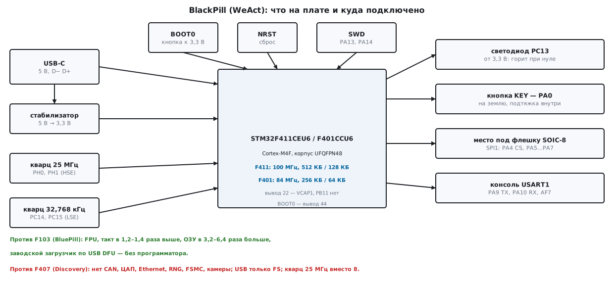
One board, two chips: the STM32F411CEU6 (more expensive and faster) and the
STM32F401CCU6. Both come in the same package — UFQFPN48, and the pin numbers match;
on the F401, pins 8 and 9 are called VSSA/VREF- and VREF+ in the CubeMX database, on the F411 —
VSSA and VDDA. What sits around the chip:
| What | Where | Source of the information |
|---|---|---|
| 25 MHz crystal | PH0, PH1 (HSE) |
STM32_HSECLK 25000000U in the QMK board settings |
| 32.768 kHz watch crystal | PC14, PC15 (LSE) |
STM32_LSECLK 32768U in the same place |
| LED | PC13, anode to 3.3 V |
the platform description in QMK: "connected to +3.3V" |
| KEY button | PA0 |
same place: "shared with the User Key" |
| BOOT0 and NRST buttons | pin 44 and pin 7 | pin assignment — CubeMX database; buttons — from the board description |
| footprint for an SOIC-8 flash | PA4 — select, PA5…PA7 — SCK, MISO, MOSI |
the platform description in QMK |
| USB-C connector | PA11, PA12 |
OTG_FS pin assignment — DocID026289 |
| SWD header | PA13 SWDIO, PA14 SWCLK |
same place |
None of this was checked against the board schematic: the regulator, the resistors and exactly what
the buttons are connected to are known here from descriptions. According to the QMK description, two pins
are taken: PB2 is BOOT1 (pin 20 according to DocID026289) and is left alone; PA9
on the F411 is also OTG_FS_VBUS.
The LED on PC13 lights on a low level. That is how it should be: according to the datasheet
(DocID026289, note to the pin table) PC13…PC15 are supplied through the backup domain
power switch, which passes only 3 mA, the speed is no higher than 2 MHz at
30 pF, and these pins must not be used as a current source for an LED.
So the pin only sinks current: the LED goes from 3.3 V to the pin. The same was true of the
BluePill (2.6), and the register code for the LED carries over from it without changes —
except for the port address.
Not all pins tolerate 5 V. On the F411, two pins out of 36 — PA0 and PB5 — are marked
TC, "Standard 3.3 V I/O", in the datasheet; the rest are FT. On the F401, according to DS9716, both
PA0 and PB5 are FT. The KEY button sits exactly on PA0: if you
use its pin for a 5 V sensor, that is a mistake on the F411, but not on the F401.
2ж.2 F411 and F401 versus F103 and F407
A summary from the CubeMX chip database: what exists in this package — peripheral
instances, frequency, memory, number of I/O lines (the section's chips.py,
its output saved in full):
| F103C8 (BluePill) | F401CC (BlackPill) | F411CE (BlackPill) | F407VG (Discovery) | |
|---|---|---|---|---|
| package | LQFP48 | UFQFPN48 | UFQFPN48 | LQFP100 |
| core | M3 | M4F | M4F | M4F |
| frequency, MHz | 72 | 84 | 100 | 168 |
| Flash, KB | 64 (CB — 128) | 256 (CB — 128) | 512 (CC — 256) | 1024 (VE — 512) |
| RAM, KB | 20 | 64 | 128 | 128 + 64 CCM |
| I/O lines | 37 | 36 | 36 | 82 |
| USART/UART | 3 | 3 | 3 | 6 |
| SPI / I²S | 2 / 0 | 3 / 2 | 5 / 5 | 3 / 2 |
| I²C | 2 | 3 | 3 | 3 |
| timers | 4 | 8 | 8 | 14 |
| ADC | 2 | 1 | 1 | 3 |
| DAC | — | — | — | 1 |
| CAN | 1 | — | — | 2 |
| Ethernet | — | — | — | 1 |
| USB | FS, device only | OTG FS | OTG FS | OTG FS + OTG HS |
| SDIO | — | — | 1 | 1 |
| FSMC, RNG, camera | — | — | — | yes |
The "Flash" and "RAM" rows agree with Table 2 of both datasheets: F411xE has 512 KB and 128 KB, F401xC has 256 KB and 64 KB. The main points of the table:
- No CAN, DAC or Ethernet. Sections 15, 19 and 105–106а cannot be repeated on the BlackPill; CAN only with an external controller on SPI.
- There is no USART3, but there is USART6. Code from the BluePill with the console on
USART3(PB10/PB11) does not carry over directly:PB11does not exist in this package at all. - The F411 has five SPIs, the F401 has three in this package. Yet the
stm32f401xc.hheader declares bothSPI4andSDIO: the F401 has them in packages from 64 pins up (DS9716, Table 2), but not in UFQFPN48. The header speaks for the family, not for the package. - 8 timers: TIM1–TIM5 and TIM9–TIM11. The basic TIM6/TIM7, which the handbook often uses to trigger the ADC, are absent.
What is declared in the CMSIS headers themselves (the same script looks for a #define with
the block name):
stm32f401xc.h: SPI4 USB_OTG_FS SDIO CRC I2S2ext
  нет: CAN1 DAC1 ETH RNG DCMI FSMC_Bank1 TIM6 TIM8 USART3 UART4 SPI5 USB_OTG_HS
stm32f411xe.h: SPI4 SPI5 USB_OTG_FS SDIO CRC I2S2ext
  нет: CAN1 DAC1 ETH RNG DCMI FSMC_Bank1 TIM6 TIM8 USART3 UART4 USB_OTG_HS
stm32f407xx.h: CAN1 DAC1 ETH RNG DCMI FSMC_Bank1 TIM6 TIM8 USART3 UART4 USB_OTG_HS USB_OTG_FS SDIO CRC I2S2ext
  нет: SPI4 SPI5
So a porting error shows up already at build time: the line CAN1->MCR = … will not compile
with stm32f411xe.h.
Pins by number. The BluePill and BlackPill packages are different (LQFP and UFQFPN, 2.9), but ST uses a common pin numbering for the 48-pin package. A comparison from the CubeMX database — where the same number carries something else:
F411CE: 5:PD0>PH0 6:PD1>PH1 22:PB11>VCAP1
F401CC: 5:PD0>PH0 6:PD1>PH1 8:VSSA>VSSA/VREF- 9:VDDA>VREF+ 22:PB11>VCAP1
On the F4 the crystal pins are called PH0/PH1 instead of PD0/PD1, and in place of
PB11 there is VCAP1, the core regulator pin: a capacitor hangs on it, and
nothing else may be connected there. It is the same story as in 2.1 with the
F103RB and F401RE in LQFP64.
2ж.3 Clock: a 25 MHz crystal, 100 or 96 MHz and the core voltage
The Discovery has an 8 MHz crystal, the BlackPill a 25 MHz one. The first consequence is
the constant: by default system_stm32f4xx.c assumes HSE_VALUE = 25 MHz
(2.8), and on the BlackPill that value matches the board. The mistake here is the
opposite one: code carried over from the Discovery together with -DHSE_VALUE=8000000
will be off by a factor of 3.125 on the BlackPill.
The second consequence is the PLL dividers. The core frequency is HSE / M × N / P, the output
for USB is HSE / M × N / Q, and each chip has its own limits: VCO input 1–2 MHz,
VCO output 100–432 MHz (on the F401 — 192–432), Q output no higher than 48 MHz, and USB
needs exactly 48 (RM0383 and RM0368, 6.3.2; RM0090, 7.3.2). An exhaustive search over all
combinations of M, N, P, Q on the computer (pll.c):
F411 hse=25000000: configs=108510 usb48_configs=28
  max_sysclk=100.000 MHz (m=13 n=104 p=2)
  max_sysclk_usb48=96.000 MHz (m=25 n=192 p=2 q=4, vco_in=1.000 MHz)
F401 hse=25000000: configs=38683 usb48_configs=19
  max_sysclk=84.000 MHz (m=25 n=336 p=4)
  max_sysclk_usb48=84.000 MHz (m=25 n=336 p=4 q=7, vco_in=1.000 MHz)
F407 hse=8000000: configs=47128 usb48_configs=130
  max_sysclk=168.000 MHz (m=4 n=168 p=2)
  max_sysclk_usb48=168.000 MHz (m=4 n=168 p=2 q=7, vco_in=2.000 MHz)
F411_hse8 hse=8000000: configs=41218 usb48_configs=110
  max_sysclk=100.000 MHz (m=4 n=100 p=2)
  max_sysclk_usb48=96.000 MHz (m=4 n=96 p=2 q=4, vco_in=2.000 MHz)
The F411 cannot run at 100 MHz and have USB at the same time. This is not a property of the
crystal: the last line is the same F411 with an 8 MHz crystal, and its ceiling with USB is
also 96 MHz. The reason is arithmetic: at 100 MHz on the core, VCO = 100 × P,
that is 200 or 400 MHz (800 is already beyond the limit), and for USB the VCO must
divide by 48 exactly — neither 200 nor 400 does. So the F411 with USB
runs at 96 MHz, while the F401 at its 84 MHz gets USB with no loss. QMK
does the same: the settings of the BLACKPILL_STM32_F411 board have PLLM 25,
PLLN 384, PLLP 4, PLLQ 8 — that is 96 MHz and 48 MHz; for the F401 — 25, 336, 4,
7, that is 84 and 48.
The 25 MHz crystal has a price too: exactly 48 MHz is obtained only with M = 25 (25 · N = 48 · M · Q, and 25 and 48 are coprime), so the VCO input is 1 MHz, the lower edge of the range. RM0383 recommends 2 MHz "to limit PLL jitter", but with such a crystal and USB that cannot be reached. Without USB the F411 reaches 100 MHz also with 1.923 MHz at the input (M = 13).
Everything that depends on the board is collected in board.h. For the F411:
#if defined(BOARD_BLACKPILL_F411)
#define BOARD_NAME   "BlackPill F411CE"
#define CHIP_HEADER  "stm32f411xe.h"
#define HSE_HZ       25000000u      /* кварц 25 МГц на плате */
#if defined(CLOCK_USB)              /* для USB нужен ровно 48 МГц с выхода Q */
#define PLL_M        25u            /* 25 / 25 = 1 МГц на входе VCO */
#define PLL_N        384u           /* VCO 384 МГц */
#define PLL_P        4u             /* SYSCLK 96 МГц */
#define PLL_Q        8u             /* 48 МГц — USB годится */
#else
#define PLL_M        25u
#define PLL_N        400u           /* VCO 400 МГц */
#define PLL_P        4u             /* SYSCLK 100 МГц — предел F411 */
#define PLL_Q        9u             /* 44,4 МГц — не выше 48, но для USB не годится */
#endif
#define FLASH_WS     3u             /* RM0383, таблица 5: 90 < HCLK <= 100 МГц при 2,7–3,6 В */
#define VOS_BITS     3u             /* PWR_CR.VOS = 11, Scale 1, до 100 МГц; после сброса 10 — до 84 */
#define APB1_DIV     2u             /* APB1 не выше 50 МГц */
#define APB2_DIV     1u             /* APB2 не выше 100 МГц */
Core voltage. On the F411 the VOS field in PWR_CR is two bits wide, and after reset
it holds 10 — Scale 2, up to 84 MHz (RM0383, 5.4.1). 100 MHz needs 11 — Scale 1, and
it can be written only while the PLL is off. On the F401 Scale 2 is the ceiling of
84 MHz, and the value 11 is reserved. On the F407 VOS is the single bit 14, and after
reset it is already 1, Scale 1 (RM0090, 5.4.1). That is why F407 code that
does not touch VOS works on the F407, but leaves the F411 at 100 MHz on the step
for up to 84 MHz — outside the specification.
Flash wait states at 2.7–3.6 V: on the F411, 3 cycles for 90–100 MHz (RM0383,
Table 5), on the F401, 2 cycles for 60–84 MHz (RM0368, Table 6), on the F407, 5 for
150–168 MHz (RM0090, Table 10). The test_board.c check is built for
each board and compares the numbers in board.h with these tables and with the bus limits:
board=BlackPill F411CE chip=F411 hse=25000000 m=25 n=400 p=4 q=9
  vco_in=1000000 vco=400000000 sysclk=100000000 pclk1=50000000 pclk2=100000000 q_out=44444444 ws_need=3 ws=3
The whole setup is one function. The order follows RM0383 (3.4.1 and section 6): crystal, core voltage, PLL, Flash wait states with a check, bus dividers, switching. Every wait is bounded: if the crystal does not start, the function returns a code and the core stays on the 16 MHz HSI — the console will report it by itself.
int clock_init(void)
{
    RCC->CR |= RCC_CR_HSEON;
    if (wait_set(&RCC->CR, RCC_CR_HSERDY)) {
        RCC->CR &= ~RCC_CR_HSEON;
        return CLOCK_NO_HSE;                           /* кварца нет или он не завёлся */
    }

    RCC->APB1ENR |= RCC_APB1ENR_PWREN;
    (void)RCC->APB1ENR;                                /* дождаться включения такта PWR */
    PWR->CR = (PWR->CR & ~(3u << 14)) | VOS_BITS << 14; /* VOS меняется только при выключенной PLL */

    RCC->PLLCFGR = (RCC->PLLCFGR & ~CLK_PLLCFGR_FIELDS)   /* бит 29 после сброса — 1, он резервный */
                 | clk_pllcfgr(PLL_M, PLL_N, PLL_P, PLL_Q, CLK_SRC_HSE);
    RCC->CR |= RCC_CR_PLLON;
    if (wait_set(&RCC->CR, RCC_CR_PLLRDY))
        return CLOCK_NO_PLL;

    FLASH->ACR = FLASH_ACR_ICEN | FLASH_ACR_DCEN | FLASH_ACR_PRFTEN | FLASH_WS;
    if ((FLASH->ACR & FLASH_ACR_LATENCY) != FLASH_WS)   /* RM0383, 3.4.1: прочитать и убедиться */
        return CLOCK_NO_WS;

    RCC->CFGR = (RCC->CFGR & ~(RCC_CFGR_HPRE | RCC_CFGR_PPRE1 | RCC_CFGR_PPRE2))
              | clk_cfgr_div(1u, APB1_DIV, APB2_DIV);   /* делители — до переключения */
    RCC->CFGR = (RCC->CFGR & ~RCC_CFGR_SW) | RCC_CFGR_SW_PLL;
    for (uint32_t n = 0; (RCC->CFGR & RCC_CFGR_SWS) != RCC_CFGR_SWS_PLL; n++)
        if (n >= WAIT_LOOPS)
            return CLOCK_NO_SW;
    SystemCoreClock = SYSCLK_HZ;
    return CLOCK_OK;
}
The reserved bit in RCC_PLLCFGR. After reset it holds 0x24003010 (RM0383,
6.3.2): M = 16, N = 192, P = 2, Q = 4 — and also a one in bit 29, which
is described as reserved. Writing "the whole register" would clear it, and reserved
bits are supposed to be left as they are. So clk_pllcfgr assembles the fields, and
the rest is preserved with a mask:
clk: reset=0x24003010 fields(16,192,2,4,HSI)=0x04003010 reserved=0x20000000 with_reserved=0x24003010 src=0 sysclk=16000000
The same file clk.c decodes the registers back into frequencies. It is called by
the console command clk (2ж.6), and the check on the computer builds the register values
from board.h and compares the decoding with the expected frequencies:
RCC_PLLCFGR=0x09416419 RCC_CFGR=0x00001008 -> sysclk=100000000 hclk=100000000 pclk1=50000000 pclk2=100000000 pll48=44444444
| Board | SYSCLK | APB1 / APB2 | USB | RCC_PLLCFGR (fields) |
wait states | VOS |
|---|---|---|---|---|---|---|
| BlackPill F411 | 100 MHz | 50 / 100 MHz | 44.4 MHz — not usable | 0x09416419 |
3 | 11 |
BlackPill F411, -DCLOCK_USB |
96 MHz | 48 / 96 MHz | 48 MHz | 0x08416019 |
3 | 11 |
| BlackPill F401 | 84 MHz | 42 / 84 MHz | 48 MHz | 0x07415419 |
2 | 10 |
| Discovery F407 | 168 MHz | 42 / 84 MHz | 48 MHz | 0x07405408 |
5 | bit 14 = 1 |
On the chip the register will hold 0x20000000 more: bit 29 stays
a one. All four builds passed the check in full (result_…=PASS).
2ж.4 How to flash: USB DFU without a programmer, and SWD
Over USB, with the factory bootloader. On the F401 and F411 the ST bootloader is written in system memory from
address 0x1FFF0000; on the F411 it takes 30424 bytes
(AN2606, Table 56). It is entered with "pattern1": BOOT0 = 1 and
BOOT1 = 0 during reset (AN2606, 26.1; RM0383, Table 2). BOOT1 is
PB2, and on the board it is already low, so on the BlackPill two
buttons are enough:
- hold BOOT0;
- press and release NRST;
- release BOOT0.
The bootloader chooses the interface itself — the one where it first sees a sign of life (AN2606, Figure 33). Of the list for the F411 (Table 56), not all pins exist in the UFQFPN48 package:
bootloader_F411CE: USART1=есть USART2=нет I2C1=есть I2C2=есть I2C3=есть SPI1=есть SPI2=есть SPI3=нет DFU=есть
The bootloader's USART2 is on PD5/PD6, SPI3 on PC10…PC12; this package
has no such pins. For USB the bootloader requires an external crystal with a frequency
that is a multiple of 1 MHz, from 4 to 26 MHz; it measures it with timer TIM11 and switches
the core to 60 MHz from the PLL. 25 MHz falls into this range. No external pull-up
resistor on D+ is needed. The computer will see the device 0483:DF11, and the firmware
is written like this (the line from the settings of the stm32-dfu bootloader in QMK):
dfu-util -d 0483:DF11 -a 0 -s 0x08000000:leave -D console_f411.bin
The :leave option starts the firmware after writing. Three more details from
Table 56 of AN2606 that explain how the bootloader behaves:
- RAM. The first 12 KB from
0x20000000are taken by the bootloader itself; write commands can access RAM from0x20003000(Table 68). - Voltage. The bootloader sets the 1.62–2.1 V range, and in it Flash is written only one byte at a time. The range is changed with bootloader commands.
- The crystal is supervised. For DFU the CSS is enabled: the crystal is lost — reset.
The chip can be identified through the bootloader by the device number and version
(Table 68): F401xB/C — PID 0x423, bootloader ID 0xD1; F411 —
0x431 and 0xD0; F407 — 0x413. These are the same numbers that the identification
function from 2а reads; the same place says what to do if the number is wrong.
How long to wait after reset before talking to the bootloader: for the F401 and F411, AN2606 (Table 69) gives at least 74.5 ms for startup and 85 ms for the crystal search.
Over UART with the same bootloader. USART1 on PA9/PA10 — 8 bits, parity,
1 stop bit, the baud rate is detected from 0x7F. This is the same as on the F407 in 48д.4–48д.5,
and the utility from there works without changes. The console of the section's examples sits on
the same pins: one USB–UART adapter serves both the console and flashing.
Over SWD. The SWD header on the board is SWDIO, SWCLK, ground and 3.3 V; any
ST-LINK will do (2.7). The commands are as in 35б, the chip file is the same as for the F407:
openocd -f interface/stlink.cfg -f target/stm32f4x.cfg -c "program console_f411.elf verify reset exit"
Neither dfu-util nor openocd was run with a board in this section: there was no real
board. The commands are taken from QMK and section 35б.
2ж.5 First project: startup code and a blinker with a button
The project has no HAL and no libraries, as in 4в: startup code in C, a linker script, CMSIS headers. There are three differences from the F103: the vector table is the same, but the FPU must be enabled before the first floating-point instruction; the linker script matches the size of its own chip; and at the end of RAM space is left for the "into the bootloader" flag (2ж.7).
void Reset_Handler(void)
{
    boot_early();                                     /* до .data и .bss: признак лежит вне них */
    for (uint32_t *s = &_sidata, *d = &_sdata; d < &_edata;)
        *d++ = *s++;
    for (uint32_t *d = &_sbss; d < &_ebss;)
        *d++ = 0u;
#ifndef NO_FPU_ENABLE
    *(volatile uint32_t *)0xE000ED88u |= 0xFu << 20;  /* SCB->CPACR: CP10 и CP11 — полный доступ */
    __asm volatile("dsb\n isb" ::: "memory");         /* до первой команды FPU */
#endif
    main();
    for (;;) {
    }
}
The linker script is a common part plus one file per chip. The flag gets the last 16 bytes of RAM, the stack grows down from it:
/* sections.ld — раздел 2ж: общая часть скрипта компоновщика для F401CC, F411CE и F407VG.
 * Память задаёт файл кристалла (f411ce.ld и др.), он же подключает этот файл.
 * Последние 16 байт ОЗУ — не стек и не .bss: там признак «в загрузчик», он переживает сброс. */
ENTRY(Reset_Handler)

_boot_flag = ORIGIN(RAM) + LENGTH(RAM) - 16;
_estack = _boot_flag;                         /* стек растёт вниз от признака */
/* f411ce.ld — раздел 2ж: STM32F411CE — 512 КБ Flash, 128 КБ ОЗУ (DocID026289, таблица 2). */
MEMORY
{
    FLASH (rx)  : ORIGIN = 0x08000000, LENGTH = 512K
    RAM   (rwx) : ORIGIN = 0x20000000, LENGTH = 128K
}
INCLUDE sections.ld
In the built images the flag ended up where expected: on the F411 — 0x2001FFF0,
on the F401 with its 64 KB — 0x2000FFF0.
The build options are for a Cortex-M4 with FPU: -mcpu=cortex-m4 -mthumb
-mfpu=fpv4-sp-d16 -mfloat-abi=hard -Os, plus -fno-math-errno, so that
the square root from sqrtf becomes a single instruction, and -fno-tree-loop-distribute-patterns:
without it GCC replaced the loops that copy .data and clear .bss with calls to
memcpy and memset, and there is no library in the build — the linker answered
undefined reference to 'memcpy'.
Pins are driven through the MODER, PUPDR, BSRR, IDR registers; the GPIO port is the same on the F401, F411 and
F407 (RM0383 and RM0090, 8.4), only the port and pin
numbers change:
static inline void pin_mode(GPIO_TypeDef *g, uint32_t pin, uint32_t mode, uint32_t pupd)
{
    port_clock(g);
    g->MODER = (g->MODER & ~(3u << 2 * pin)) | mode << 2 * pin;     /* 00 вход, 01 выход, 10 альт. функция */
    g->PUPDR = (g->PUPDR & ~(3u << 2 * pin)) | pupd << 2 * pin;     /* 00 нет, 01 вверх, 10 вниз */
}
Example 1 — a blinker with a button. A short press of KEY switches the speed (500, 250, 100 ms), a long one pauses. Debouncing is by time: the level is trusted once it has not changed for 20 ms; a long press is 800 ms.
enum key_event key_step(struct key *k, int pressed, uint32_t now_ms)
{
    uint8_t r = pressed ? 1u : 0u;
    if (r != k->raw) {                                   /* дребезг или настоящее изменение — ждём */
        k->raw = r;
        k->t_change = now_ms;
        return KEY_NONE;
    }
    if (r != k->stable && now_ms - k->t_change >= KEY_STABLE_MS) {
        k->stable = r;
        if (r) {                                         /* нажатие подтвердилось */
            k->t_down = now_ms;
            k->long_sent = 0u;
            return KEY_NONE;
        }
        return k->long_sent ? KEY_NONE : KEY_SHORT;      /* отпустили: короткое, если долгого не было */
    }
    if (k->stable && !k->long_sent && now_ms - k->t_down >= KEY_LONG_MS) {
        k->long_sent = 1u;
        return KEY_LONG;
    }
    return KEY_NONE;
}
The main loop of the blinker knows only the names from board.h about the board:
        switch (key_step(&k, pin_read(KEY_PORT, KEY_PIN) == KEY_DOWN, now)) {
        case KEY_SHORT: mode = (mode + 1u) % 3u; next = now; break;
        case KEY_LONG: paused = !paused; next = now; break;
        default: break;
        }
On the BlackPill KEY_DOWN = 0 (button to ground, internal pull-up), on the Discovery
it is 1 (button B1 to the supply, pull-down on the board, as in 198л). On the
computer the button was run through 200 presses with bounce up to 8 ms and
holds of 30–700 or 900–1500 ms, and then through 1000 single glitches
of 1–15 ms:
key: presses=200 want_short=110 got_short=110 want_long=90 got_long=90 worst_confirm_ms=28 glitches=1000 glitch_events=0
All 110 short and 90 long presses were recognised, no glitch became a press, and a press is confirmed no later than 28 ms after the first contact: 8 ms of bounce and 20 ms of quiet. The blinker was not run in QEMU: the netduinoplus2 machine has no GPIO model, its ports read as zeros.
2ж.6 Example 2: a UART console
The console is on USART1 (PA9 TX, PA10 RX, alternate function 7),
115 200 bit/s. On the Discovery — USART2 on PA2/PA3, as in section 16.
The divider is computed not from constants but from the clock that actually
came out: if the crystal did not start and the core stayed on HSI, the console will still
talk at the right baud rate.
static void uart_init(void)
{
#if CON_APB == 2u
    RCC->APB2ENR |= RCC_APB2ENR_USART1EN;
#else
    RCC->APB1ENR |= RCC_APB1ENR_USART2EN;
#endif
    pin_af(GPIOA, CON_TX_PIN, 7u);                    /* AF7 — USART1 и USART2 на всех трёх кристаллах */
    pin_af(GPIOA, CON_RX_PIN, 7u);
    GPIOA->PUPDR |= 1u << 2 * CON_RX_PIN;             /* RX с подтяжкой: без переходника не ловит шум */
    struct clk_info ci;
    clock_now(&ci);                                   /* делитель — от того такта, что вышел на самом деле */
    CON_USART->BRR = clk_brr(CON_APB == 2u ? ci.pclk2 : ci.pclk1, BAUD);
    CON_USART->CR1 = USART_CR1_UE | USART_CR1_TE | USART_CR1_RE;
}
With 16x oversampling the divider is the bus frequency divided by the baud rate, rounded. The baud rate error at all frequencies of the section is below 0.12 %:
brr: pclk=16000000 brr=139 baud=115108 err=-0.080%
brr: pclk=42000000 brr=365 baud=115068 err=-0.114%
brr: pclk=84000000 brr=729 baud=115226 err=+0.023%
brr: pclk=96000000 brr=833 baud=115246 err=+0.040%
brr: pclk=100000000 brr=868 baud=115207 err=+0.006%
The 42 MHz line is USART2 on the F407, and its BRR = 365 matches the table in 16.
Commands: help, ver, clk (clocks from the registers), id (chip number,
Flash size and unique ID), led on|off|blink, fpu (the square root of
two on the FPU), dfu (into the bootloader, 2ж.7). Line parsing is a separate file
with no hardware access; on the computer it passed 13 cases, including
backspace in both codes (0x08 and 0x7F), an extra word and a 40-character line:
cmd led on 5             -> BADARG  arg=1 buf="led on 5" ok
cmd ledon                -> UNKNOWN arg=0 buf="ledon" ok
cmd dfx<BS>u             -> DFU     arg=0 buf="dfu" ok
cmd fpz<DEL>u, LF        -> FPU     arg=0 buf="fpu" ok
cmd 40 x                 -> TOOLONG arg=0 buf="xxxxxxxxxxxxxxxxxxxxxxxxxxxxxxx" ok
The clk command takes the frequencies from RCC_CFGR and RCC_PLLCFGR with the same clk_decode:
static void cmd_clk(void)
{
    static const char *const src[] = {"HSI", "HSE", "PLL"};
    struct clk_info ci;
    clock_now(&ci);
    puts_("ядро от ");
    puts_(src[ci.src]);
    if (ci.src == CLK_SRC_PLL) {
        puts_(" (вход ");
        puts_(src[ci.pll_src]);
        puts_(")");
    }
    put_mhz(": SYSCLK ", ci.sysclk);
    put_mhz(", HCLK ", ci.hclk);
    put_mhz(", APB1 ", ci.pclk1);
    put_mhz(", APB2 ", ci.pclk2);
    if (ci.src == CLK_SRC_PLL)
        put_mhz(", USB ", ci.pll48);
    puts_("\nFLASH_ACR.LATENCY ");
    put_dec(FLASH->ACR & FLASH_ACR_LATENCY);
    puts_(", PWR_CR.VOS ");
    put_dec(PWR->CR >> 14 & 3u);
    puts_("\n");
}
The run in QEMU. The image is the same as for the board — console_f411.elf without
any special options. The netduinoplus2 machine has no RCC, PWR or Flash interface blocks,
their registers read as zeros. So the crystal "does not start", and the firmware honestly
says so — it will behave the same way on a board with an unsoldered crystal:
BlackPill F411CE 2zh-1.0
такт: кварц не запустился, работаю от HSI 16 МГц
> help
help ver clk id led on|off|blink fpu dfu
> ver
BlackPill F411CE 2zh-1.0
> clk
ядро от HSI: SYSCLK 16 МГц, HCLK 16 МГц, APB1 16 МГц, APB2 16 МГц
FLASH_ACR.LATENCY 0, PWR_CR.VOS 0
> led on
ok
> led blink
ok
> led on 5
? аргумент
> fpu
sqrt(2) = 1.414214
> foo
? help — список команд
> xxxxxxxxxxxxxxxxxxxxxxxxxxxxxxx
? строка длиннее 31 символа
The root was computed with a single instruction: in the disassembly of console_f411.elf
the vsqrt.f32 instruction occurs 1 time. The F401 image answered the same way in QEMU,
only with the name BlackPill F401CC. What clk prints on the board is not
checked here. If everything is right, it will be 100 MHz, APB1 50, APB2 100, USB 44.4
and LATENCY 3.
id crashes in QEMU — and that is useful to see. The machine returns the device number in
DBGMCU_IDCODE as zero, and it has no area with the Flash size and
unique ID (0x1FFF7A10…) at all. The read gives a
BusFault, and the handler prints the fault registers:
> id
DEV_ID 0x000, REV_ID 0x0000, Flash
HardFault: CFSR 0x00008200, HFSR 0x40000000, BFAR 0x1FFF7A22
CFSR = 0x00008200 is a precise bus error (PRECISERR) with a valid address
(BFARVALID), BFAR is the address FLASHSIZE_BASE, HFSR = 0x40000000 —
the fault was escalated to HardFault (FORCED): there is no BusFault handler. On the board
id should print DEV_ID 0x431 on the F411 or 0x423 on the F401, the Flash
size in kilobytes and the 96-bit ID; this was not checked on a board.
2ж.7 Example 3: into the bootloader on command, and what USB needs
BOOT0 is handy on the desk, but inside an enclosure it cannot be reached. The dfu command
sends the chip into the factory bootloader by itself: it puts a flag at the end of RAM and
performs a software reset. In the first line of Reset_Handler, while nothing is yet
enabled, the flag is checked, and control goes to system memory.
The reset has restored the clocks and peripherals by itself — both methods (with and without a reset)
are covered in detail in 48д.3; here is the short version for the F401 and F411:
void boot_request(void)
{
    _boot_flag[0] = BOOT_MAGIC;
    _boot_flag[1] = ~BOOT_MAGIC;                    /* второе слово: мусор в ОЗУ после включения не сойдёт за признак */
    __DSB();
    NVIC_SystemReset();
}

void boot_early(void)
{
    if (_boot_flag[0] != BOOT_MAGIC || _boot_flag[1] != ~BOOT_MAGIC)
        return;
    _boot_flag[0] = 0u;                             /* прочитали — стёрли, иначе после выхода из загрузчика снова туда */
    _boot_flag[1] = 0u;
    RCC->APB2ENR |= RCC_APB2ENR_SYSCFGEN;
    (void)RCC->APB2ENR;
    SYSCFG->MEMRMP = 1u;                            /* MEM_MODE = 01: по адресу 0 — системная память */
    SCB->VTOR = SYSMEM;
    __DSB();
    __ISB();
    uint32_t sp = ((const volatile uint32_t *)SYSMEM)[0];
    uint32_t pc = ((const volatile uint32_t *)SYSMEM)[1];
    __asm volatile("msr msp, %0\n"
                   "bx %1\n"
                   :
                   : "r"(sp), "r"(pc)
                   : "memory");
    for (;;) {
    }
}
The flag address is set by the linker script — each chip has its own, while
the code is the same. Before the reset the console waits for the TC flag: otherwise the last byte
of the message will not have time to leave on the line.
The experiment in QEMU. The machine has no system memory, so the
-DQEMU_FAKE_SYSMEM build supplies its own two-word table — the stack pointer
0x20001000 and the handler address — and the handler prints the state in which
it received the chip:
> dfu
ухожу в загрузчик: dfu-util -d 0483:df11

[системная память] MSP 0x20000FF8, VTOR 0x08001200, признак 0x00000000, PRIMASK 0x00000000
After the reset QEMU left RAM as it was, the flag was found, and boot_early
erased it. VTOR points to the supplied table, interrupts are enabled
(PRIMASK = 0). MSP is taken from the table; it is 8 bytes below 0x20001000
because the handler's prologue had already saved two registers. This chain was not checked with the real
bootloader on a board.
USB CDC on the BlackPill. A USB device of its own with a virtual COM port and a keyboard is fully built in 198ш on the U585 — it has the same OTG_FS block. This section does not port it here in full, but the documents show what will have to change:
| U585 (198ш) | F411 and F401 | |
|---|---|---|
| endpoints besides the control endpoint | 5 IN and 5 OUT | 3 IN and 3 OUT (RM0383, 22) — 198ш uses exactly three numbers: 1, 2, 3 |
| FIFO memory | 1.25 KB | 1.25 KB, the same layout |
| 48 MHz | HSI48 without a crystal | only from PLLQ: a crystal is mandatory (20.2), F411 — 96 MHz core |
| VBUS | its own enable bit | the NOVBUSSENS bit in OTG_FS_GCCFG: "VBUS is always present" — that is what QMK does (BOARD_OTG_NOVBUSSENS) |
| pins | PA11, PA12 |
PA11, PA12, alternate function 10 |
The rest — descriptors, endpoint 0, CDC — does not depend on the chip. On the F411
this is built with -DCLOCK_USB: a 96 MHz clock and exactly 48 MHz for USB
(2ж.3). The console and the blinker do not change with this clock — the UART divider
is computed from the actual frequency.
2ж.8 Porting an example from the Discovery F407
The same blink.c and console.c are built for three boards — only
the -DBOARD_… option and the linker script change. Everything that has to be touched
when porting is collected in board.h:
| Discovery F407 | BlackPill F411 | BlackPill F401 | |
|---|---|---|---|
| header | stm32f407xx.h |
stm32f411xe.h |
stm32f401xc.h |
| crystal | 8 MHz | 25 MHz | 25 MHz |
| PLL M, N, P, Q | 8, 336, 2, 7 | 25, 400, 4, 9 (with USB 25, 384, 4, 8) | 25, 336, 4, 7 |
| SYSCLK | 168 MHz | 100 MHz (96) | 84 MHz |
| Flash wait states | 5 | 3 | 2 |
| VOS | bit 14 = 1 (already after reset) | 11 — must be written | 10 (after reset) |
| APB1 / APB2, dividers | /4, /2 | /2, /1 | /2, /1 |
| LED | PD12, lit on a high level |
PC13, lit on a low level |
PC13, lit on a low level |
| button | PA0, pressed — 1, pull-down on the board |
PA0, pressed — 0, internal pull-up |
the same |
| console | USART2, PA2/PA3, APB1 |
USART1, PA9/PA10, APB2 |
the same |
| Flash / RAM in the script | 1024 K / 128 K | 512 K / 128 K | 256 K / 64 K |
The block addresses are the same on all three: GPIO from 0x40020000 on AHB1, RCC, USART1 and
USART2 in the same places. Register-level peripheral code carries over without changes;
what changes is the clock, the pin numbers and whatever the new chip lacks. Build
sizes:
   1116       4       4    1124     464 blink_f411.elf
   1116       4       4    1124     464 blink_f401.elf
   1116       4       4    1124     464 blink_f407.elf
   3416       4       8    3428     d64 console_f411.elf
   3416       4       8    3428     d64 console_f401.elf
   3408       4       8    3420     d5c console_f407.elf
The columns are code with constants, .data, .bss. The blinker on all three boards is
1116 bytes, the .bin image is 1120 bytes. The console is 3416 bytes on the BlackPill and 3408
on the Discovery, the images are 3420 and 3412 bytes. The F411 build with -DCLOCK_USB is the same
size: 3416. All nine builds of the section passed without warnings
(-Wall -Wextra -Werror).
What to do with code for what the BlackPill lacks:
- CAN, DAC, Ethernet, camera, FSMC, RNG — will not compile, and that is good: the compiler will show every place. The replacement is external chips or another board.
- TIM6/TIM7 as the ADC trigger — replace with TIM2…TIM5 using the TRGO output.
- USART3 — move to USART1, USART2 or USART6.
- The crystal and HSE_VALUE — 25 MHz, not 8; in a HAL project — in
stm32f4xx_hal_conf.h(2.8). - Size — the 128 KB of RAM on the F411 is enough for the Discovery examples, the F401 has 64 KB of RAM, and large buffers from the F407 examples may not fit; the F4x1 has no CCM at all.
2ж.9 Pitfalls
The board is "not visible" over USB in bootloader mode. According to the QMK description, the
PA10 pin with something connected to it prevents the bootloader from selecting DFU: a
pull-up resistor of about 22 kΩ is needed. From Figure 33 of AN2606 the reason is clear —
the bootloader listens on both USART1 and USB and goes wherever it first
sees something. The same description says that because of the 25 MHz crystal the board may fail to enter the
bootloader, and warming it up helps. Both observations are from QMK and were not
checked in this section.
Code from the Discovery gets timing wrong by a factor of 3.125. The
-DHSE_VALUE=8000000 was left in, while the BlackPill crystal is 25 MHz. HAL delays and
the UART baud rate will drift; the clock setup function of this section will not
notice, because it computes from board.h, not from HSE_VALUE.
100 MHz and USB do not work together. The Q output at a 400 MHz VCO gives 44.4 MHz,
and the device will not enumerate. For USB the F411 runs at 96 MHz (-DCLOCK_USB),
2ж.3.
The F411 at 100 MHz without writing VOS. After reset VOS = 10 — the step for up to
84 MHz. F407 code, where Scale 1 is already set after reset, skips this step.
It may even work on the desk, but it is outside the specification; write VOS before enabling the
PLL.
HardFault on the very first floating-point instruction. The FPU was not enabled in
CPACR. The -DNO_FPU_ENABLE build in QEMU on the fpu command:
> fpu

HardFault: CFSR 0x00080000, HFSR 0x40000000, BFAR 0x00000000
CFSR = 0x00080000 is the NOCP bit (UsageFault, "no coprocessor"),
escalated to HardFault. This error does not happen on the F103: it has no FPU, and the
compiler with -mfloat-abi=soft emits no floating-point instructions. Without enabling the
FPU the image is 24 bytes smaller (3392 versus 3416) — exactly the size of that enabling code.
memcpy in a program without libraries. At -Os, GCC recognises a call to memcpy in the
loop that copies .data, and memset in the one that clears .bss. Without a
library the build fails at link time; the cure is
-fno-tree-loop-distribute-patterns (2ж.5).
The header promises what the package does not have. stm32f401xc.h declares
SPI4 and SDIO, stm32f411xe.h — also all five SPIs on all the pins of the
family. In UFQFPN48 the F401 has three SPIs and no SDIO, and the pins PB11, PC10…PC12,
PD5/PD6 do not exist on either of the two. Check against the pin table of the datasheet or against
CubeMX, not against the header.
The LED is "inverted". PC13 lights on a low level, while PD12 on the Discovery lights on a
high one. In board.h it is a single LED_ON line; in code scattered across the
project it is a dozen places.
A 5 V sensor on PA0. On the F411, PA0 and PB5 do not tolerate 5 V (2ж.1). On the F401,
according to DS9716, they do — the board is the same, but the answer differs.
Garbage after power-up taken for the bootloader flag. One word is not enough: RAM is not cleared after power is applied. So the flag is two words, a magic value and its complement, and it is erased right after it is read. Otherwise the device would go back into the bootloader again after leaving it.
2ж.10 Summary
- BlackPill is an F411CE (100 MHz, 512 KB Flash, 128 KB RAM) or an F401CC (84 MHz,
256 and 64 KB) in UFQFPN48, Cortex-M4F, 25 MHz and 32.768 kHz crystals, an LED on
PC13(lit on a low level), the KEY button onPA0, USB-C, BOOT0 and NRST buttons. - Versus the F103: FPU, a clock 1.2–1.4 times higher, 3.2–6.4 times more RAM, three I²C and OTG FS. Versus the F407: no CAN, DAC, Ethernet, RNG, FSMC, camera, USART3 or TIM6/TIM7; 36 I/O lines versus 82.
- On the 48-pin F4, pins 5, 6 and 22 carry
PH0,PH1andVCAP1— where the F103C8 hasPD0,PD1andPB11. - Clock: F411 — 100 MHz without USB or 96 MHz with USB (M 25, N 384, P 4, Q 8),
100 MHz and 48 MHz together cannot be reached with any crystal; F401 — 84 and 48 MHz.
For 100 MHz —
VOS= 11 and 3 Flash wait states. - Flashing without a programmer: BOOT0 + NRST, device
0483:DF11,dfu-util … -s 0x08000000:leave; the bootloader needs a 4–26 MHz crystal, a multiple of 1 MHz, it clocks the core from the PLL at 60 MHz and writes Flash one byte at a time. - Three examples from the same sources for three boards: the blinker — 1116 bytes of code,
the console — 3416 bytes (3408 on the F407); in QEMU the console answered all
commands,
fpugave1.414214with a singlevsqrt.f32instruction, without enabling the FPU —NOCPinCFSR(0x00080000). - Logic on the computer: the button — 200 presses without a single error, 1000 glitches without false presses; command parsing — 13 cases; UART divider — error below 0.12 % at all frequencies of the section.
- Into the bootloader on command: a flag in the last 16 bytes of RAM (
0x2001FFF0on the F411,0x2000FFF0on the F401), a reset, a jump in the first line ofReset_Handler.
Full sources
Everything needed to build and repeat the examples: board settings, clock, startup
code and linker scripts, the three examples and the PLL search. The checks on the
computer (test_board.c, test_logic.c), the substitute system memory
for QEMU, the CubeMX database parser and the run scripts are in the source archive of the
section. The CMSIS headers come from the STM32F4xx_DFP pack.
board.h — everything in which the three boards differ: clock, wait states, VOS, LED, button, console.
/* board.h — раздел 2ж: всё, чем три платы отличаются друг от друга, в одном месте.
 * Собирать с одним из -DBOARD_BLACKPILL_F411, -DBOARD_BLACKPILL_F401, -DBOARD_DISC_F407.
 * Здесь только числа и имена: файл читает и прошивка, и проверка на компьютере.
 * Такты — по RM0383 (F411), RM0368 (F401), RM0090 (F407); выводы — по описанию плат. */
#ifndef BOARD_H
#define BOARD_H

#if defined(BOARD_BLACKPILL_F411)
#define BOARD_NAME   "BlackPill F411CE"
#define CHIP_HEADER  "stm32f411xe.h"
#define HSE_HZ       25000000u      /* кварц 25 МГц на плате */
#if defined(CLOCK_USB)              /* для USB нужен ровно 48 МГц с выхода Q */
#define PLL_M        25u            /* 25 / 25 = 1 МГц на входе VCO */
#define PLL_N        384u           /* VCO 384 МГц */
#define PLL_P        4u             /* SYSCLK 96 МГц */
#define PLL_Q        8u             /* 48 МГц — USB годится */
#else
#define PLL_M        25u
#define PLL_N        400u           /* VCO 400 МГц */
#define PLL_P        4u             /* SYSCLK 100 МГц — предел F411 */
#define PLL_Q        9u             /* 44,4 МГц — не выше 48, но для USB не годится */
#endif
#define FLASH_WS     3u             /* RM0383, таблица 5: 90 < HCLK <= 100 МГц при 2,7–3,6 В */
#define VOS_BITS     3u             /* PWR_CR.VOS = 11, Scale 1, до 100 МГц; после сброса 10 — до 84 */
#define APB1_DIV     2u             /* APB1 не выше 50 МГц */
#define APB2_DIV     1u             /* APB2 не выше 100 МГц */
#define LED_PORT     GPIOC
#define LED_PIN      13u
#define LED_ON       0u             /* светодиод от 3,3 В к PC13: горит при нуле на выводе */
#define KEY_PORT     GPIOA
#define KEY_PIN      0u
#define KEY_DOWN     0u             /* кнопка KEY замыкает PA0 на землю */
#define KEY_PUPD     1u             /* PUPDR = 01: подтяжка вверх внутри кристалла */
#define CON_USART    USART1         /* PA9 TX, PA10 RX — те же, что у заводского загрузчика */
#define CON_APB      2u
#define CON_TX_PIN   9u
#define CON_RX_PIN   10u

#elif defined(BOARD_BLACKPILL_F401)
#define BOARD_NAME   "BlackPill F401CC"
#define CHIP_HEADER  "stm32f401xc.h"
#define HSE_HZ       25000000u
#define PLL_M        25u            /* 1 МГц на входе VCO */
#define PLL_N        336u           /* VCO 336 МГц: у F401 не ниже 192 */
#define PLL_P        4u             /* SYSCLK 84 МГц — предел F401 */
#define PLL_Q        7u             /* 48 МГц — USB годится на той же частоте */
#define FLASH_WS     2u             /* RM0368, таблица 6: 60 < HCLK <= 84 МГц при 2,7–3,6 В */
#define VOS_BITS     2u             /* VOS = 10, Scale 2, до 84 МГц — значение после сброса */
#define APB1_DIV     2u             /* APB1 не выше 42 МГц */
#define APB2_DIV     1u             /* APB2 не выше 84 МГц */
#define LED_PORT     GPIOC
#define LED_PIN      13u
#define LED_ON       0u
#define KEY_PORT     GPIOA
#define KEY_PIN      0u
#define KEY_DOWN     0u
#define KEY_PUPD     1u
#define CON_USART    USART1
#define CON_APB      2u
#define CON_TX_PIN   9u
#define CON_RX_PIN   10u

#elif defined(BOARD_DISC_F407)
#define BOARD_NAME   "Discovery F407VG"
#define CHIP_HEADER  "stm32f407xx.h"
#define HSE_HZ       8000000u       /* кварц 8 МГц на Discovery */
#define PLL_M        8u             /* 1 МГц на входе VCO */
#define PLL_N        336u           /* VCO 336 МГц */
#define PLL_P        2u             /* SYSCLK 168 МГц */
#define PLL_Q        7u             /* 48 МГц */
#define FLASH_WS     5u             /* RM0090, таблица 10: 150 < HCLK <= 168 МГц при 2,7–3,6 В */
#define VOS_BITS     1u             /* у F405/F407 VOS — один бит 14: 1 = Scale 1, значение после сброса */
#define APB1_DIV     4u             /* APB1 42 МГц */
#define APB2_DIV     2u             /* APB2 84 МГц */
#define LED_PORT     GPIOD
#define LED_PIN      12u            /* зелёный LD4 */
#define LED_ON       1u
#define KEY_PORT     GPIOA
#define KEY_PIN      0u
#define KEY_DOWN     1u             /* синяя кнопка B1: нажатие — высокий уровень */
#define KEY_PUPD     0u             /* подтяжка вниз стоит на плате */
#define CON_USART    USART2         /* PA2 TX, PA3 RX, как в разделе 16 */
#define CON_APB      1u
#define CON_TX_PIN   2u
#define CON_RX_PIN   3u

#else
#error "BOARD_BLACKPILL_F411, BOARD_BLACKPILL_F401 или BOARD_DISC_F407"
#endif

#define SYSCLK_HZ    (HSE_HZ / PLL_M * PLL_N / PLL_P)
#define HCLK_HZ      SYSCLK_HZ
#define PCLK1_HZ     (HCLK_HZ / APB1_DIV)
#define PCLK2_HZ     (HCLK_HZ / APB2_DIV)
#define CON_PCLK_HZ  (CON_APB == 2u ? PCLK2_HZ : PCLK1_HZ)

#endif
clk.h — clock arithmetic: the fields of RCC_PLLCFGR and RCC_CFGR.
/* clk.h — раздел 2ж: арифметика тактов STM32F4 без доступа к железу.
 * Поля RCC_PLLCFGR и RCC_CFGR одинаковы у F401, F411 и F407 (RM0368 и RM0383 — 6.3.2–6.3.3, RM0090 — 7.3.2–7.3.3),
 * поэтому один и тот же код и собирает значение регистра, и разбирает его обратно в частоты. */
#ifndef CLK_H
#define CLK_H
#include <stdint.h>

#define CLK_SRC_HSI 0u
#define CLK_SRC_HSE 1u
#define CLK_SRC_PLL 2u

#define CLK_PLLCFGR_FIELDS 0x0F437FFFu   /* M, N, P, SRC, Q; остальные биты резервные — не трогать */

struct clk_info {
    uint32_t src;        /* что сейчас тактирует ядро: CLK_SRC_* по полю SWS */
    uint32_t pll_src;    /* вход PLL: CLK_SRC_HSI или CLK_SRC_HSE */
    uint32_t sysclk, hclk, pclk1, pclk2, pll48;   /* Гц; pll48 — выход Q для USB */
};

uint32_t clk_pllcfgr(uint32_t m, uint32_t n, uint32_t p, uint32_t q, uint32_t src);
uint32_t clk_cfgr_div(uint32_t ahb, uint32_t apb1, uint32_t apb2);
void clk_decode(uint32_t cfgr, uint32_t pllcfgr, uint32_t hse_hz, struct clk_info *ci);
uint32_t clk_brr(uint32_t pclk, uint32_t baud);

#endif
clk.c — assembling register values and decoding them back into frequencies, the USART divider.
/* clk.c — раздел 2ж: значения RCC_PLLCFGR и RCC_CFGR и обратный разбор в частоты.
 * Поля по RM0383 (6.3.2 RCC_PLLCFGR, 6.3.3 RCC_CFGR); у F401 (RM0368, 6.3) и F407 (RM0090, 7.3) они те же. */
#include "clk.h"

#define HSI_HZ 16000000u

uint32_t clk_pllcfgr(uint32_t m, uint32_t n, uint32_t p, uint32_t q, uint32_t src)
{
    return (m & 0x3Fu)                                 /* PLLM: биты 5:0 */
         | (n & 0x1FFu) << 6                           /* PLLN: биты 14:6 */
         | ((p / 2u - 1u) & 3u) << 16                  /* PLLP: 00 = 2, 01 = 4, 10 = 6, 11 = 8 */
         | (src == CLK_SRC_HSE ? 1u : 0u) << 22        /* PLLSRC */
         | (q & 0xFu) << 24;                           /* PLLQ: биты 27:24 */
}

static uint32_t ahb_code(uint32_t div)
{
    static const uint16_t d[] = {2, 4, 8, 16, 64, 128, 256, 512};
    for (uint32_t i = 0; i < 8u; i++)
        if (d[i] == div)
            return 8u + i;                             /* 1000 = /2 … 1111 = /512 */
    return 0u;                                         /* 0xxx = без деления */
}

static uint32_t apb_code(uint32_t div)
{
    switch (div) {
    case 2u: return 4u;                                /* 100 */
    case 4u: return 5u;
    case 8u: return 6u;
    case 16u: return 7u;
    default: return 0u;                                /* 0xx = без деления */
    }
}

uint32_t clk_cfgr_div(uint32_t ahb, uint32_t apb1, uint32_t apb2)
{
    return ahb_code(ahb) << 4 | apb_code(apb1) << 10 | apb_code(apb2) << 13;
}

static uint32_t ahb_div(uint32_t code)
{
    static const uint16_t d[] = {2, 4, 8, 16, 64, 128, 256, 512};
    return code & 8u ? d[code & 7u] : 1u;
}

static uint32_t apb_div(uint32_t code)
{
    return code & 4u ? 2u << (code & 3u) : 1u;
}

void clk_decode(uint32_t cfgr, uint32_t pllcfgr, uint32_t hse_hz, struct clk_info *ci)
{
    uint32_t m = pllcfgr & 0x3Fu, n = pllcfgr >> 6 & 0x1FFu;
    uint32_t p = ((pllcfgr >> 16 & 3u) + 1u) * 2u, q = pllcfgr >> 24 & 0xFu;
    uint32_t in, vco;

    ci->pll_src = pllcfgr & (1u << 22) ? CLK_SRC_HSE : CLK_SRC_HSI;
    in = ci->pll_src == CLK_SRC_HSE ? hse_hz : HSI_HZ;
    vco = m ? in / m * n : 0u;                          /* делим первым: 25 МГц · 400 не влезает в 32 бита */
    ci->pll48 = q ? vco / q : 0u;
    switch (cfgr >> 2 & 3u) {                           /* SWS: чем тактируется ядро на самом деле */
    case 1u: ci->src = CLK_SRC_HSE; ci->sysclk = hse_hz; break;
    case 2u: ci->src = CLK_SRC_PLL; ci->sysclk = vco / p; break;
    default: ci->src = CLK_SRC_HSI; ci->sysclk = HSI_HZ; break;
    }
    ci->hclk = ci->sysclk / ahb_div(cfgr >> 4 & 0xFu);
    ci->pclk1 = ci->hclk / apb_div(cfgr >> 10 & 7u);
    ci->pclk2 = ci->hclk / apb_div(cfgr >> 13 & 7u);
}

uint32_t clk_brr(uint32_t pclk, uint32_t baud)
{
    return (pclk + baud / 2u) / baud;                   /* OVER8 = 0: BRR = f / скорость, с округлением */
}
clock.h — return codes of the clock setup.
/* clock.h — раздел 2ж: настройка тактов платы и чтение того, что вышло на самом деле. */
#ifndef CLOCK_H
#define CLOCK_H
#include <stdint.h>
#include "clk.h"

#define CLOCK_OK      0
#define CLOCK_NO_HSE  1     /* кварц не запустился — работаем от HSI 16 МГц */
#define CLOCK_NO_PLL  2
#define CLOCK_NO_WS   3     /* задержки Flash не записались */
#define CLOCK_NO_SW   4

extern uint32_t SystemCoreClock;

int clock_init(void);
void clock_now(struct clk_info *ci);

#endif
clock.c — the clock from the crystal through the PLL with bounded waits.
/* clock.c — раздел 2ж: такт от кварца через PLL на трёх платах, регистрами CMSIS.
 * Порядок — по RM0383, 3.4.1 и 6.3: напряжение ядра (VOS) до включения PLL, задержки Flash до
 * переключения на PLL, проверка каждого шага по флагу. Кварц может не запуститься — тогда остаёмся
 * на HSI 16 МГц и говорим об этом, а не висим в цикле. */
#include "board.h"
#include CHIP_HEADER
#include "clk.h"
#include "clock.h"

#define WAIT_LOOPS 200000u        /* опросов флага; HSE по даташиту встаёт за ~2 мс (DocID026289, таблица 37) */

uint32_t SystemCoreClock = 16000000u;

static int wait_set(volatile uint32_t *reg, uint32_t mask)
{
    for (uint32_t n = 0; n < WAIT_LOOPS; n++)
        if (*reg & mask)
            return 0;
    return -1;
}

int clock_init(void)
{
    RCC->CR |= RCC_CR_HSEON;
    if (wait_set(&RCC->CR, RCC_CR_HSERDY)) {
        RCC->CR &= ~RCC_CR_HSEON;
        return CLOCK_NO_HSE;                           /* кварца нет или он не завёлся */
    }

    RCC->APB1ENR |= RCC_APB1ENR_PWREN;
    (void)RCC->APB1ENR;                                /* дождаться включения такта PWR */
    PWR->CR = (PWR->CR & ~(3u << 14)) | VOS_BITS << 14; /* VOS меняется только при выключенной PLL */

    RCC->PLLCFGR = (RCC->PLLCFGR & ~CLK_PLLCFGR_FIELDS)   /* бит 29 после сброса — 1, он резервный */
                 | clk_pllcfgr(PLL_M, PLL_N, PLL_P, PLL_Q, CLK_SRC_HSE);
    RCC->CR |= RCC_CR_PLLON;
    if (wait_set(&RCC->CR, RCC_CR_PLLRDY))
        return CLOCK_NO_PLL;

    FLASH->ACR = FLASH_ACR_ICEN | FLASH_ACR_DCEN | FLASH_ACR_PRFTEN | FLASH_WS;
    if ((FLASH->ACR & FLASH_ACR_LATENCY) != FLASH_WS)   /* RM0383, 3.4.1: прочитать и убедиться */
        return CLOCK_NO_WS;

    RCC->CFGR = (RCC->CFGR & ~(RCC_CFGR_HPRE | RCC_CFGR_PPRE1 | RCC_CFGR_PPRE2))
              | clk_cfgr_div(1u, APB1_DIV, APB2_DIV);   /* делители — до переключения */
    RCC->CFGR = (RCC->CFGR & ~RCC_CFGR_SW) | RCC_CFGR_SW_PLL;
    for (uint32_t n = 0; (RCC->CFGR & RCC_CFGR_SWS) != RCC_CFGR_SWS_PLL; n++)
        if (n >= WAIT_LOOPS)
            return CLOCK_NO_SW;
    SystemCoreClock = SYSCLK_HZ;
    return CLOCK_OK;
}

void clock_now(struct clk_info *ci)
{
    clk_decode(RCC->CFGR, RCC->PLLCFGR, HSE_HZ, ci);
}
startup.c — vector table, Reset_Handler, enabling the FPU.
/* startup.c — раздел 2ж: стартовый код для STM32F401, F411 и F407 без библиотек.
 * Таблица векторов — до SysTick: прерывания периферии примеры не используют.
 * После сброса: признак «в загрузчик» (boot_early), копия .data, обнуление .bss, включение FPU, main. */
#include <stdint.h>
#include "boot.h"

extern uint32_t _estack, _sidata, _sdata, _edata, _sbss, _ebss;
int main(void);

void Default_Handler(void)
{
    for (;;) {
    }
}

void NMI_Handler(void) __attribute__((weak, alias("Default_Handler")));
void HardFault_Handler(void) __attribute__((weak, alias("Default_Handler")));
void SysTick_Handler(void) __attribute__((weak, alias("Default_Handler")));

void Reset_Handler(void)
{
    boot_early();                                     /* до .data и .bss: признак лежит вне них */
    for (uint32_t *s = &_sidata, *d = &_sdata; d < &_edata;)
        *d++ = *s++;
    for (uint32_t *d = &_sbss; d < &_ebss;)
        *d++ = 0u;
#ifndef NO_FPU_ENABLE
    *(volatile uint32_t *)0xE000ED88u |= 0xFu << 20;  /* SCB->CPACR: CP10 и CP11 — полный доступ */
    __asm volatile("dsb\n isb" ::: "memory");         /* до первой команды FPU */
#endif
    main();
    for (;;) {
    }
}

__attribute__((section(".isr_vector"), used))
const void *const vectors[16] = {
    &_estack,              /* начальный указатель стека */
    Reset_Handler,
    NMI_Handler,
    HardFault_Handler,
    Default_Handler,       /* MemManage */
    Default_Handler,       /* BusFault */
    Default_Handler,       /* UsageFault */
    0, 0, 0, 0,
    Default_Handler,       /* SVCall */
    Default_Handler,       /* DebugMon */
    0,
    Default_Handler,       /* PendSV */
    SysTick_Handler,
};
sections.ld — the common part of the linker script, the flag at the end of RAM.
/* sections.ld — раздел 2ж: общая часть скрипта компоновщика для F401CC, F411CE и F407VG.
 * Память задаёт файл кристалла (f411ce.ld и др.), он же подключает этот файл.
 * Последние 16 байт ОЗУ — не стек и не .bss: там признак «в загрузчик», он переживает сброс. */
ENTRY(Reset_Handler)

_boot_flag = ORIGIN(RAM) + LENGTH(RAM) - 16;
_estack = _boot_flag;                         /* стек растёт вниз от признака */

SECTIONS
{
    .isr_vector : { KEEP(*(.isr_vector)) } > FLASH
    .text : { *(.text*) *(.rodata*) . = ALIGN(4); } > FLASH
    .ARM.exidx : { *(.ARM.exidx*) } > FLASH
    _sidata = LOADADDR(.data);
    .data : { _sdata = .; *(.data*) . = ALIGN(4); _edata = .; } > RAM AT > FLASH
    .bss (NOLOAD) : { _sbss = .; *(.bss*) *(COMMON) . = ALIGN(4); _ebss = .; } > RAM
}
f411ce.ld — STM32F411CE memory.
/* f411ce.ld — раздел 2ж: STM32F411CE — 512 КБ Flash, 128 КБ ОЗУ (DocID026289, таблица 2). */
MEMORY
{
    FLASH (rx)  : ORIGIN = 0x08000000, LENGTH = 512K
    RAM   (rwx) : ORIGIN = 0x20000000, LENGTH = 128K
}
INCLUDE sections.ld
f401cc.ld — STM32F401CC memory.
/* f401cc.ld — раздел 2ж: STM32F401CC — 256 КБ Flash, 64 КБ ОЗУ (DS9716, таблица 2). */
MEMORY
{
    FLASH (rx)  : ORIGIN = 0x08000000, LENGTH = 256K
    RAM   (rwx) : ORIGIN = 0x20000000, LENGTH = 64K
}
INCLUDE sections.ld
f407vg.ld — STM32F407VG memory.
/* f407vg.ld — раздел 2ж: STM32F407VG — 1 МБ Flash, 128 КБ основного ОЗУ; CCM 64 КБ не используется. */
MEMORY
{
    FLASH (rx)  : ORIGIN = 0x08000000, LENGTH = 1024K
    RAM   (rwx) : ORIGIN = 0x20000000, LENGTH = 128K
}
INCLUDE sections.ld
io.h — pins through CMSIS registers.
/* io.h — раздел 2ж: выводы F4 регистрами CMSIS. У F401, F411 и F407 порт GPIO устроен одинаково:
 * MODER, OTYPER, OSPEEDR, PUPDR, IDR, BSRR, AFR[2] (RM0383, 8.4; RM0090, 8.4). Подключать после CHIP_HEADER. */
#ifndef IO_H
#define IO_H
#include <stdint.h>

static inline void port_clock(GPIO_TypeDef *g)
{
    RCC->AHB1ENR |= 1u << (((uint32_t)g - GPIOA_BASE) / 0x400u);   /* GPIOAEN — бит 0, GPIOBEN — 1, … */
    (void)RCC->AHB1ENR;
}

static inline void pin_mode(GPIO_TypeDef *g, uint32_t pin, uint32_t mode, uint32_t pupd)
{
    port_clock(g);
    g->MODER = (g->MODER & ~(3u << 2 * pin)) | mode << 2 * pin;     /* 00 вход, 01 выход, 10 альт. функция */
    g->PUPDR = (g->PUPDR & ~(3u << 2 * pin)) | pupd << 2 * pin;     /* 00 нет, 01 вверх, 10 вниз */
}

static inline void pin_af(GPIO_TypeDef *g, uint32_t pin, uint32_t af)
{
    pin_mode(g, pin, 2u, 0u);
    g->AFR[pin >> 3] = (g->AFR[pin >> 3] & ~(0xFu << 4 * (pin & 7u))) | af << 4 * (pin & 7u);
}

static inline void pin_write(GPIO_TypeDef *g, uint32_t pin, uint32_t level)
{
    g->BSRR = level ? 1u << pin : 1u << (pin + 16u);                /* одна запись, без чтения порта */
}

static inline uint32_t pin_read(GPIO_TypeDef *g, uint32_t pin)
{
    return g->IDR >> pin & 1u;
}

#endif
key.h — the button: events and state.
/* key.h — раздел 2ж: кнопка с антидребезгом, короткое и долгое нажатие. Без доступа к железу. */
#ifndef KEY_H
#define KEY_H
#include <stdint.h>

#define KEY_STABLE_MS 20u      /* столько уровень должен не меняться, чтобы ему поверить */
#define KEY_LONG_MS   800u     /* дольше — долгое нажатие */

enum key_event { KEY_NONE, KEY_SHORT, KEY_LONG };

struct key {
    uint8_t raw, stable;       /* последний прочитанный и подтверждённый уровень: 1 — нажата */
    uint8_t long_sent;
    uint32_t t_change, t_down; /* когда менялся сырой уровень, когда подтвердилось нажатие */
};

void key_init(struct key *k);
enum key_event key_step(struct key *k, int pressed, uint32_t now_ms);

#endif
key.c — debouncing, short and long press.
/* key.c — раздел 2ж: антидребезг по времени. Звать раз в миллисекунду с сырым уровнем кнопки.
 * Короткое нажатие сообщается при отпускании, долгое — как только кнопку продержали KEY_LONG_MS. */
#include "key.h"

void key_init(struct key *k)
{
    k->raw = k->stable = k->long_sent = 0u;
    k->t_change = k->t_down = 0u;
}

enum key_event key_step(struct key *k, int pressed, uint32_t now_ms)
{
    uint8_t r = pressed ? 1u : 0u;
    if (r != k->raw) {                                   /* дребезг или настоящее изменение — ждём */
        k->raw = r;
        k->t_change = now_ms;
        return KEY_NONE;
    }
    if (r != k->stable && now_ms - k->t_change >= KEY_STABLE_MS) {
        k->stable = r;
        if (r) {                                         /* нажатие подтвердилось */
            k->t_down = now_ms;
            k->long_sent = 0u;
            return KEY_NONE;
        }
        return k->long_sent ? KEY_NONE : KEY_SHORT;      /* отпустили: короткое, если долгого не было */
    }
    if (k->stable && !k->long_sent && now_ms - k->t_down >= KEY_LONG_MS) {
        k->long_sent = 1u;
        return KEY_LONG;
    }
    return KEY_NONE;
}
blink.c — example 1: the blinker and the button.
/* blink.c — раздел 2ж, пример 1: мигалка и кнопка регистрами CMSIS — один файл на три платы.
 * Короткое нажатие KEY — следующая скорость (500, 250, 100 мс), долгое — пауза и обратно.
 * Всё, что зависит от платы (вывод, уровень «горит», подтяжка, такт), — в board.h. */
#include "board.h"
#include CHIP_HEADER
#include "io.h"
#include "clock.h"
#include "key.h"

static volatile uint32_t ms;
void SysTick_Handler(void) { ms++; }

static void led(int on)
{
    pin_write(LED_PORT, LED_PIN, on ? LED_ON : !LED_ON);
}

int main(void)
{
    static const uint16_t period[] = {500, 250, 100};
    struct key k;
    uint32_t mode = 0, paused = 0, lit = 0, next = 0, last = 0;

    clock_init();                                       /* не вышло — мигаем от HSI, SysTick считает сам */
    SysTick_Config(SystemCoreClock / 1000u);
    pin_mode(LED_PORT, LED_PIN, 1u, 0u);
    led(0);
    pin_mode(KEY_PORT, KEY_PIN, 0u, KEY_PUPD);
    key_init(&k);

    for (;;) {
        uint32_t now = ms;
        if (now == last)
            continue;                                   /* кнопку — раз в миллисекунду */
        last = now;
        switch (key_step(&k, pin_read(KEY_PORT, KEY_PIN) == KEY_DOWN, now)) {
        case KEY_SHORT: mode = (mode + 1u) % 3u; next = now; break;
        case KEY_LONG: paused = !paused; next = now; break;
        default: break;
        }
        if (paused) {
            led(0);
        } else if ((int32_t)(now - next) >= 0) {
            lit = !lit;
            led(lit);
            next = now + period[mode];
        }
    }
}
cmd.h — the console line and commands.
/* cmd.h — раздел 2ж: строка консоли и разбор команды. Без доступа к железу. */
#ifndef CMD_H
#define CMD_H

#define LINE_MAX 32u           /* с завершающим нулём: 31 символ */

enum cmd_id { CMD_EMPTY, CMD_HELP, CMD_VER, CMD_CLK, CMD_ID, CMD_LED, CMD_FPU, CMD_DFU, CMD_UNKNOWN, CMD_BADARG,
              CMD_TOOLONG };

struct line {
    char buf[LINE_MAX];
    unsigned len;
    int overflow;              /* строка оказалась длиннее буфера — выполнять нельзя */
};

struct cmd {
    enum cmd_id id;
    int arg;                   /* led: 0 — off, 1 — on, 2 — blink */
};

void line_init(struct line *l);
int line_feed(struct line *l, char c, char *echo);   /* 1 — строка готова; echo — что вернуть в терминал */
struct cmd cmd_parse(const struct line *l);

#endif
cmd.c — a line with echo and backspace, command parsing.
/* cmd.c — раздел 2ж: строка консоли с эхом и забоем, разбор «команда [аргумент]».
 * Один и тот же файл собирается в прошивку и в проверку на компьютере. */
#include "cmd.h"

void line_init(struct line *l)
{
    l->len = 0u;
    l->overflow = 0;
}

int line_feed(struct line *l, char c, char *echo)
{
    echo[0] = 0;
    if (c == '\r' || c == '\n') {
        l->buf[l->len < LINE_MAX ? l->len : LINE_MAX - 1u] = 0;
        echo[0] = '\r', echo[1] = '\n', echo[2] = 0;
        return 1;
    }
    if (c == '\b' || c == 0x7F) {                     /* забой: терминалы шлют то одно, то другое */
        if (l->len && !l->overflow) {
            l->len--;
            echo[0] = '\b', echo[1] = ' ', echo[2] = '\b', echo[3] = 0;
        }
        return 0;
    }
    if (c < ' ')
        return 0;                                     /* прочие управляющие — мимо */
    if (l->len < LINE_MAX - 1u) {
        l->buf[l->len++] = c;
        echo[0] = c, echo[1] = 0;
    } else {
        l->overflow = 1;                              /* лишнее не храним, но и строку не выполним */
    }
    return 0;
}

static int word(const char **p, const char *w)
{
    const char *s = *p;
    while (*w && *s == *w)
        s++, w++;
    if (*w || (*s && *s != ' '))
        return 0;
    while (*s == ' ')
        s++;
    *p = s;
    return 1;
}

struct cmd cmd_parse(const struct line *l)
{
    struct cmd c = {CMD_UNKNOWN, 0};
    const char *s = l->buf;
    if (l->overflow) {
        c.id = CMD_TOOLONG;
        return c;
    }
    while (*s == ' ')
        s++;
    if (!*s)
        c.id = CMD_EMPTY;
    else if (word(&s, "help"))
        c.id = CMD_HELP;
    else if (word(&s, "ver"))
        c.id = CMD_VER;
    else if (word(&s, "clk"))
        c.id = CMD_CLK;
    else if (word(&s, "id"))
        c.id = CMD_ID;
    else if (word(&s, "fpu"))
        c.id = CMD_FPU;
    else if (word(&s, "dfu"))
        c.id = CMD_DFU;
    else if (word(&s, "led")) {
        c.id = CMD_LED;
        if (word(&s, "off"))
            c.arg = 0;
        else if (word(&s, "on"))
            c.arg = 1;
        else if (word(&s, "blink"))
            c.arg = 2;
        else
            c.id = CMD_BADARG;
        if (c.id == CMD_LED && *s)
            c.id = CMD_BADARG;                        /* «led on 5» — лишнее слово */
        return c;
    }
    if (c.id != CMD_UNKNOWN && c.id != CMD_EMPTY && *s)
        c.id = CMD_BADARG;                            /* у остальных команд аргументов нет */
    return c;
}
console.c — examples 2 and 3: the UART console and the dfu command.
/* console.c — раздел 2ж, примеры 2 и 3: консоль по UART и уход в USB DFU по команде.
 * BlackPill: USART1 на PA9/PA10, Discovery: USART2 на PA2/PA3; 115 200 бит/с, 8N1, опрос без прерываний.
 * Команды: help, ver, clk, id, led on|off|blink, fpu, dfu. */
#include "board.h"
#include CHIP_HEADER
#include "io.h"
#include "clock.h"
#include "cmd.h"
#include "boot.h"

#define VERSION "2zh-1.0"
#define BAUD    115200u

static volatile uint32_t ms;
static volatile int blink;

void SysTick_Handler(void)
{
    ms++;
    if (blink && ms % 250u == 0u)
        LED_PORT->ODR ^= 1u << LED_PIN;
}

static void putc_(char c)
{
    while (!(CON_USART->SR & USART_SR_TXE)) {
    }
    CON_USART->DR = (uint8_t)c;
}

static void puts_(const char *s)
{
    for (; *s; s++) {
        if (*s == '\n')
            putc_('\r');
        putc_(*s);
    }
}

static void raw(const char *s)
{
    for (; *s; s++)
        putc_(*s);
}

static void put_dec(uint32_t v)
{
    char b[11];
    int i = 10;
    b[i] = 0;
    do {
        b[--i] = (char)('0' + v % 10u);
        v /= 10u;
    } while (v);
    puts_(b + i);
}

static void put_hex(uint32_t v, int digits)
{
    puts_("0x");
    while (digits--)
        putc_("0123456789ABCDEF"[v >> 4 * digits & 0xFu]);
}

static void put_mhz(const char *name, uint32_t hz)
{
    puts_(name);
    put_dec(hz / 1000000u);
    if (hz % 1000000u) {                              /* 44,4 МГц и подобные — с одним знаком */
        putc_(',');
        put_dec(hz % 1000000u / 100000u);
    }
    puts_(" МГц");
}

static void uart_init(void)
{
#if CON_APB == 2u
    RCC->APB2ENR |= RCC_APB2ENR_USART1EN;
#else
    RCC->APB1ENR |= RCC_APB1ENR_USART2EN;
#endif
    pin_af(GPIOA, CON_TX_PIN, 7u);                    /* AF7 — USART1 и USART2 на всех трёх кристаллах */
    pin_af(GPIOA, CON_RX_PIN, 7u);
    GPIOA->PUPDR |= 1u << 2 * CON_RX_PIN;             /* RX с подтяжкой: без переходника не ловит шум */
    struct clk_info ci;
    clock_now(&ci);                                   /* делитель — от того такта, что вышел на самом деле */
    CON_USART->BRR = clk_brr(CON_APB == 2u ? ci.pclk2 : ci.pclk1, BAUD);
    CON_USART->CR1 = USART_CR1_UE | USART_CR1_TE | USART_CR1_RE;
}

static void cmd_clk(void)
{
    static const char *const src[] = {"HSI", "HSE", "PLL"};
    struct clk_info ci;
    clock_now(&ci);
    puts_("ядро от ");
    puts_(src[ci.src]);
    if (ci.src == CLK_SRC_PLL) {
        puts_(" (вход ");
        puts_(src[ci.pll_src]);
        puts_(")");
    }
    put_mhz(": SYSCLK ", ci.sysclk);
    put_mhz(", HCLK ", ci.hclk);
    put_mhz(", APB1 ", ci.pclk1);
    put_mhz(", APB2 ", ci.pclk2);
    if (ci.src == CLK_SRC_PLL)
        put_mhz(", USB ", ci.pll48);
    puts_("\nFLASH_ACR.LATENCY ");
    put_dec(FLASH->ACR & FLASH_ACR_LATENCY);
    puts_(", PWR_CR.VOS ");
    put_dec(PWR->CR >> 14 & 3u);
    puts_("\n");
}

static void cmd_id(void)
{
    const volatile uint32_t *uid = (const volatile uint32_t *)UID_BASE;
    puts_("DEV_ID ");
    put_hex(DBGMCU->IDCODE & 0xFFFu, 3);              /* 0x423 — F401xB/C, 0x431 — F411, 0x413 — F407 */
    puts_(", REV_ID ");
    put_hex(DBGMCU->IDCODE >> 16, 4);
    puts_(", Flash ");
    put_dec(*(const volatile uint16_t *)FLASHSIZE_BASE);
    puts_(" КБ, UID ");
    put_hex(uid[2], 8);
    put_hex(uid[1], 8);
    put_hex(uid[0], 8);
    puts_("\n");
}

static void cmd_fpu(void)
{
    volatile float x = 2.0f;                          /* volatile: не дать компилятору сосчитать заранее */
    float r = __builtin_sqrtf(x);                     /* одна команда VSQRT.F32 с -fno-math-errno */
    puts_("sqrt(2) = ");
    uint32_t u = (uint32_t)(r * 1000000.0f + 0.5f);  /* миллионные доли, с округлением */
    put_dec(u / 1000000u);
    putc_('.');
    for (uint32_t d = 100000u; d; d /= 10u)           /* шесть знаков, с ведущими нулями */
        putc_((char)('0' + u / d % 10u));
    puts_("\n");
}

static void run(struct cmd c)
{
    switch (c.id) {
    case CMD_EMPTY: break;
    case CMD_HELP: puts_("help ver clk id led on|off|blink fpu dfu\n"); break;
    case CMD_VER: puts_(BOARD_NAME " " VERSION "\n"); break;
    case CMD_CLK: cmd_clk(); break;
    case CMD_ID: cmd_id(); break;
    case CMD_FPU: cmd_fpu(); break;
    case CMD_LED:
        blink = c.arg == 2;
        if (c.arg < 2)
            pin_write(LED_PORT, LED_PIN, c.arg ? LED_ON : !LED_ON);
        puts_("ok\n");
        break;
    case CMD_DFU:
        puts_("ухожу в загрузчик: dfu-util -d 0483:df11\n");
        while (!(CON_USART->SR & USART_SR_TC)) {      /* дождаться, пока последний байт уйдёт в линию */
        }
        boot_request();
        break;
    case CMD_TOOLONG: puts_("? строка длиннее 31 символа\n"); break;
    case CMD_BADARG: puts_("? аргумент\n"); break;
    default: puts_("? help — список команд\n"); break;
    }
}

void HardFault_Handler(void)
{
    puts_("\nHardFault: CFSR ");
    put_hex(SCB->CFSR, 8);
    puts_(", HFSR ");
    put_hex(SCB->HFSR, 8);
    puts_(", BFAR ");
    put_hex(SCB->BFAR, 8);                            /* адрес, если в CFSR стоит BFARVALID */
    puts_("\n");
    for (;;) {
    }
}

int main(void)
{
    static const char *const why[] = {"", "кварц не запустился", "PLL не захватилась", "задержки Flash", "переключение"};
    int rc = clock_init();
    SysTick_Config(SystemCoreClock / 1000u);
    pin_mode(LED_PORT, LED_PIN, 1u, 0u);
    pin_write(LED_PORT, LED_PIN, !LED_ON);
    uart_init();
    puts_("\n" BOARD_NAME " " VERSION "\n");
    if (rc != CLOCK_OK) {
        puts_("такт: ");
        puts_(why[rc]);
        puts_(", работаю от HSI 16 МГц\n");
    }
    struct line l;
    line_init(&l);
    puts_("> ");
    for (;;) {
        if (!(CON_USART->SR & USART_SR_RXNE))
            continue;
        char echo[4];
        if (line_feed(&l, (char)CON_USART->DR, echo)) {
            raw(echo);
            run(cmd_parse(&l));
            line_init(&l);
            puts_("> ");
        } else {
            raw(echo);
        }
    }
}
boot.h — entering the factory bootloader from the firmware.
/* boot.h — раздел 2ж: уйти в заводской загрузчик (USB DFU) из прошивки, без кнопки BOOT0. */
#ifndef BOOT_H
#define BOOT_H

#define BOOT_MAGIC 0xDF00B007u

void boot_request(void);   /* из приложения: признак в конце ОЗУ и программный сброс */
void boot_early(void);     /* первой строкой Reset_Handler: признак есть — прыжок в системную память */

#endif
boot.c — a flag in RAM, a reset and a jump into system memory.
/* boot.c — раздел 2ж: вход в заводской загрузчик F401/F411 из прошивки — признак в ОЗУ и сброс.
 * Сброс возвращает такты и периферию в исходное состояние сам, поэтому прыжок делается первой строкой
 * Reset_Handler, пока ничего не включено (подробно оба пути — в разделе 48д.3).
 * Системная память — 0x1FFF0000 у F401, F411 и F407 (AN2606, таблица 68). */
#include "board.h"
#include CHIP_HEADER
#include "boot.h"

extern volatile uint32_t _boot_flag[2];             /* два слова в конце ОЗУ, вне .data и .bss (*.ld) */

#ifdef QEMU_FAKE_SYSMEM
extern const uint32_t fake_sysmem[2];               /* опыт в QEMU: «системная память» внутри образа */
#define SYSMEM ((uint32_t)fake_sysmem)
#else
#define SYSMEM 0x1FFF0000u
#endif

void boot_request(void)
{
    _boot_flag[0] = BOOT_MAGIC;
    _boot_flag[1] = ~BOOT_MAGIC;                    /* второе слово: мусор в ОЗУ после включения не сойдёт за признак */
    __DSB();
    NVIC_SystemReset();
}

void boot_early(void)
{
    if (_boot_flag[0] != BOOT_MAGIC || _boot_flag[1] != ~BOOT_MAGIC)
        return;
    _boot_flag[0] = 0u;                             /* прочитали — стёрли, иначе после выхода из загрузчика снова туда */
    _boot_flag[1] = 0u;
    RCC->APB2ENR |= RCC_APB2ENR_SYSCFGEN;
    (void)RCC->APB2ENR;
    SYSCFG->MEMRMP = 1u;                            /* MEM_MODE = 01: по адресу 0 — системная память */
    SCB->VTOR = SYSMEM;
    __DSB();
    __ISB();
    uint32_t sp = ((const volatile uint32_t *)SYSMEM)[0];
    uint32_t pc = ((const volatile uint32_t *)SYSMEM)[1];
    __asm volatile("msr msp, %0\n"
                   "bx %1\n"
                   :
                   : "r"(sp), "r"(pc)
                   : "memory");
    for (;;) {
    }
}
pll.c — search over M, N, P, Q of the main PLL.
/* pll.c — раздел 2ж: перебор всех M, N, P, Q главной PLL для кварца платы.
 * Ограничения — из описаний RCC_PLLCFGR: PLLM 2…63, вход VCO 1…2 МГц, PLLN 50…432 (у F401 — 192…432),
 * выход VCO 100…432 МГц (у F401 — 192…432), PLLP 2/4/6/8, PLLQ 2…15, выход Q не выше 48 МГц.
 * Вопрос: какая наибольшая SYSCLK вообще и при ровно 48 МГц для USB. */
#include <stdio.h>
#include <stdint.h>

struct chip { const char *name; uint64_t hse, sys_max, n_min, vco_min; };

static void scan(const struct chip *c)
{
    unsigned total = 0, usb = 0;
    uint64_t best_num = 0, best_den = 1, busb_num = 0, busb_den = 1;
    unsigned bm = 0, bn = 0, bp = 0, um = 0, un = 0, up = 0, uq = 0;
    for (unsigned m = 2; m <= 63; m++) {
        if (c->hse < 1000000u * m || c->hse > 2000000u * m)       /* вход VCO 1…2 МГц: hse/m */
            continue;
        for (unsigned n = (unsigned)c->n_min; n <= 432; n++) {
            uint64_t vco_x_m = c->hse * n;                         /* VCO · m — без дробей */
            if (vco_x_m < c->vco_min * m || vco_x_m > 432000000ull * m)
                continue;
            for (unsigned p = 2; p <= 8; p += 2) {
                if (vco_x_m > c->sys_max * m * p)                  /* SYSCLK = vco_x_m / (m · p) */
                    continue;
                for (unsigned q = 2; q <= 15; q++) {
                    if (vco_x_m > 48000000ull * m * q)
                        continue;                                  /* выход Q выше 48 МГц — нельзя */
                    total++;
                    int exact = vco_x_m == 48000000ull * m * q;
                    usb += exact;
                    /* сравнить дроби vco_x_m / (m·p) */
                    if (vco_x_m * best_den > best_num * m * p) {
                        best_num = vco_x_m, best_den = (uint64_t)m * p;
                        bm = m, bn = n, bp = p;
                    }
                    if (exact && (vco_x_m * busb_den > busb_num * m * p
                                  || (vco_x_m * busb_den == busb_num * m * p && m < um))) {
                        busb_num = vco_x_m, busb_den = (uint64_t)m * p;
                        um = m, un = n, up = p, uq = q;
                    }
                }
            }
        }
    }
    printf("%s hse=%llu: configs=%u usb48_configs=%u\n", c->name, (unsigned long long)c->hse, total, usb);
    printf("  max_sysclk=%.3f MHz (m=%u n=%u p=%u)\n", (double)best_num / best_den / 1e6, bm, bn, bp);
    printf("  max_sysclk_usb48=%.3f MHz (m=%u n=%u p=%u q=%u, vco_in=%.3f MHz)\n",
           (double)busb_num / busb_den / 1e6, um, un, up, uq, (double)c->hse / um / 1e6);
}

int main(void)
{
    static const struct chip chips[] = {
        {"F411", 25000000u, 100000000u, 50, 100000000u},
        {"F401", 25000000u, 84000000u, 192, 192000000u},
        {"F407", 8000000u, 168000000u, 50, 100000000u},
        {"F411_hse8", 8000000u, 100000000u, 50, 100000000u},
    };
    for (unsigned i = 0; i < sizeof chips / sizeof chips[0]; i++)
        scan(&chips[i]);
    return 0;
}
Next: section 3 "The C language for embedded systems" — types, bit operations,
volatile and why the compiler sometimes throws your code away.